Note: Descriptions are shown in the official language in which they were submitted.
CA 02514134 2005-07-22
WO 2004/070899 449 003 WO/CA
Vertilas GmbH 22 July 2005/mb/tk
Method for producing a waveguide structure in a surface
emitting semiconductor laser and surface-emitting
semiconductor laser
The invention relates to a method for producing a
waveguide structure in a surface-emitting semiconductor
laser and a semiconductor laser of this kind.
Surface-emitting laser diodes, in English: Vertical-
Cavity Surface-Emitting Lasers (VCSEL), are semiconductor
lasers in which the emission of light takes place
perpendicularly to the surface of the semiconductor chip.
Compared with conventional edge-emitting laser diodes the
surface-emitting laser diodes have numerous advantages
such as a low electrical power consumption, the
possibility of direct monitoring of the laser diode on
the wafer, ease of coupling to a glass fibre,
longitudinal single mode spectra and the possibility of
connecting the surface-emitting laser diodes together to
form a two-dimensional matrix.
In the field of communications technology using fibre
optics, because of the wavelength-dependent dispersion or
absorption, there is a need for VCSELs in a wavelength
range from about 1.3 to 2 ~,m, particularly around the
wavelength 1.31 ~,m or 1.55 Vim. Long-wave laser diodes
with useful properties, particularly for the wavelength
range above 1.3 ~,m, have up till now been produced from
InP-based connecting semiconductors. GaAs-based VCSELs
are suitable for the shorter wave range of < 1.3 Vim. The
CA 02514134 2005-07-22
- 2 -
following approaches have hitherto been tried in an
effort to solve the problem:
A continuous wave VCSEL which emits at an output of 1 mW
at 1.55 ~m is made up, for example, of an InP substrate
with metamorphic layers or mirrors (IEEE Photonics
Technology Letters, Volume 11, Number 6, June 1999, pages
629 to 631). Lateral wave guiding is achieved here by
proton implanting.
A VCSEL produced in a single epitactic growth process
with an output of 0.45 mW at a wavelength of 1.5 to 1.6
~m with a metamorphic mirror on the light emitting side
is known from "High Performance 1.6 ~m Single-Epitaxy
Top-Emitting VCSEL", (Conference on Lasers & Electro-
Optics (CLEO) 2000, San Francisco, USA, Post-Deadline
Paper CPD 12, pages 23-24). Current and wave guiding
were achieved here by selective oxidation.
A VCSEL with an air semiconductor mirror (InP air gap
DBRs, for Distributed Bragg Reflectors) is proposed in
IEEE ISLC 2002, pages 145 to 146. A tunnel junction is
applied between the active zone and the upper DBR mirror,
the current being limited by underetching of the tunnel
junction layer. The air gap surrounding the remaining
tunnel junction area serves as a waveguide for the
optical field.
Moreover, a VCSEL with antimonide-based mirrors in which
an underetched InGaAs-active zone is enclosed by two n-
doped InP layers, adjoined by AlGaAsSb-DBR mirrors, is
known from the publication on the 26th European
CA 02514134 2005-07-22
- 3 -
Conference on Optical Communication, ECOC 2000, "88°C,
Continuous-Wave Operation of 1.55 ~m Vertical-Cavity
Surface-Emitting Lasers". The selective underetching in
this case brings about lateral wave guiding.
The best properties in terms of performance, operating
temperature range, single mode power and modulation
bandwidth, however, are found in VCSELs with buried
tunnel junctions, in English: Buried Tunnel Junctions,
(BTJ). The manufacture and structure of the buried
tunnel junction will be described hereinafter with
reference to Figure 1. A highly doped p+/n+ pair of
layers 101, 102 with a small band spacing is produced by
molecular beam epitaxy (MBE). The actual tunnel junction
103 is formed between these layers. By reactive ion
etching (RIE) a circular or elliptical area is shaped,
which is essentially formed by the n+-doped layer 102,
the tunnel junction 103 and some or all of the p+-doped
layer 101. This area is overgrown with n-doped InP
(layer 104) in a second epitaxy run, so that the tunnel
junction 103 is "buried". The contact area between the
overgrown layer 104 and the p+-doped layer 101 acts as a
barrier layer when voltage is applied. The current flows
through the tunnel junction with resistances of typically
3 x 10⁻⁶ SZ cm2 . In this way the current f low can be
restricted to the actual area of the active zone 108.
Moreover, little heat is generated, as the current flows
from a high-resistance p-doped layer to a low resistance
n-doped layer.
The overgrowing of the tunnel junction leads to slight
variations in thickness which have an unfavourable effect
CA 02514134 2005-07-22
- 4 -
on lateral wave guiding, with the result that the
production of higher lateral modes is made easier,
particularly when there are fairly large apertures. For
single mode operation, which is required particularly in
fibre optic communications technology, only small
apertures can therefore be used, with a correspondingly
lower laser output.
Examples and applications of VCSELs with buried tunnel
junctions can be found for example in "Low-threshold
index-guided 1.5 ~m long wavelength vertical-cavity
surface-emitting laser with high efficiency", Applied
Physics Letter, Volume 76, Number 16, pages 2179 to 2181
of 17 April 2000, in "Long wavelength Buried-Tunnel-
Junction Vertical-Cavity Surface-Emitting Lasers", Adv.
in Solid State Phys. 41, 75 to 85, 2001, in "Vertical-
cavity surface-emitting laser diodes at 1.55 ~,m with
large output power and high operation temperature",
Electronics Letters, Volume 37, Number 21 pages 1295 to
1296 of 11 October 2001, in "90°C Continuous-Wave
Operation of 1.83 ~,m Vertical-Cavity Surface-Emitting
Lasers", IEEE Photonics Technology Letters, Volume 12,
Number 11, pages 1435 to 1437, November 2000, and in
"High-Speed modulation up to 10 Gbit/s with 1.55 ~,m
2~> wavelength InGaAlAs VCSELs", Electronics Letters, Volume
38, Number 20, 26 September 2002. Lateral wave guiding
is provided here by lateral variation in the resonator
length.
The structure of the InP-based VCSEL discussed in the
above-mentioned literature will now be briefly explained
with reference to Figure 2, starting from the structure
CA 02514134 2005-07-22
-
of the buried tunnel junction in Figure 1 described
above.
The Buried Tunnel Junction (BTJ) is arranged the other
5 way round in this structure, so that the active zone 106
is situated above the tunnel junction with the diameter
DBTJ between the p+-doped layer 101 and the n+-doped layer
102. The laser radiation travels in the direction
indicated by the arrow 116. The active zone 106 is
surrounded by a p-doped layer 105 (InAlAs) and an n-doped
layer 108 (InAlAs). The front mirror 109 above the
active zone 106 consists of an epitaxial DBR with about
35 pairs of InGaAlAs/InAlAs layers, producing a
reflectivity of about 99.4%. The rear mirror 112
consists of a stack of dielectric layers as DBR and ends
with a layer of gold, producing a reflectivity of nearly
99.75%. An insulating layer 113 prevents direct contact
of the n-InP layer 104 with the contact layer 114 at the
p-end which mostly consists of gold or silver (cf. DE 101
07 349 A1). Reference numeral 111 designates the p-end
contact layer which is annular in structure.
The combination of the dielectric mirror 112 and the
integrated contact layer 114 and heat sink 115 results in
a greatly increased heat conductivity compared with
epitaxial mufti-layer structures. Current is injected
through the contact layer 114 or through the integrated
heat sink 115 and the contact points 110 at the n-end.
For further details of the manufacture and properties of
the vCSEL types shown in Figure 2, the reader is again
expressly directed to the references mentioned above.
CA 02514134 2005-07-22
- 6 -
In the proposed VCSEL diodes, particularly for the
wavelength range between about 1.3 and 2 Vim, there is a
need to be able to adjust the lateral radiation profile
thereof within wide ranges by lateral wave guiding.
Here, too, manufacturing should take place with the usual
epitactical overgrowth, and for this reason Al-free InP-
based VCSELs, in particular, are suitable for wavelengths
above 1 Vim.
In GaAs-based VCSELs, which, however, can only be used in
wavelengths ranges below about 1.3 Vim, the lateral wave
guiding is produced by selectively oxidised AlAs layers
(cf. "Advances in Selective Wet Oxidation of AlGaAs
Alloys", in IEEE Journal of Selected Topics in Quantum
Electronics, Vol. 3, No. 3, June 1997, pages 916-926).
The VCSEL discussed therein consists of multiple layers
of GaAs-AlGaAs, produced epitactically by Metal Organic
Vapour Phase Epitaxy (MOVPE). By wet oxidation of the
AlGaAs layers, buried oxide layers are formed which leave
an unoxidised aperture open in the centre of the vCSEL.
This method has not hitherto been successfully applied to
the InP-based VCSELs, as AlAs cannot be applied or can
only be applied in too thin layers because of the
mismatching of the lattice constants, and other
oxidisable materials such as e.g. AlGaSb have hitherto
not produced an oxide layer of sufficient quality.
Therefore, with the long wave VCSELs, other methods of
lateral wave guiding have been used, such as for example
lateral variation of the resonator length, selectively
etched layers, proton implanting or metamorphic AlAs
layers, as already explained above in connection with the
references.
CA 02514134 2005-07-22
_ 7 _
The aim of the invention is to provide an in particular
InP-based surface-emitting laser diode which can be
produced cheaply and in high yields and the lateral
radiation profile of which can be adjusted within wide
ranges by lateral wave guiding. Moreover, lateral single
mode operation should be stable even with larger
apertures and should be able to achieve higher
efficiency.
This aim is achieved by the method claimed according to
the invention for producing a waveguide structure in a
surface-emitting semiconductor laser and by the surface-
emitting semiconductor layer claimed according to the
invention. Further embodiments will become apparent from
the subsidiary claims and the description that follows.
The process according to the invention for producing a
waveguide structure in a surface-emitting semiconductor
laser with an active zone having a pn transition,
surrounded by a first n-doped semiconductor layer and at
least one p-doped semiconductor layer, and with a tunnel
junction on the p-side of the active zone which is
adjacent to a second n-doped semiconductor layer,
proposes first of all applying, in a first epitactic
growth process, an n-doped barrier layer onto the minimum
of one p-doped semiconductor layer, this n-doped barrier
layer subsequently being at least partly removed in order
to form an aperture, and then, in a second epitactic
growth process, applying the layer provided for the
tunnel junction to the barrier layer and the aperture.
CA 02514134 2005-07-22
The process according to the invention thus results in
the following epitactic structure outside the area of the
aperture (from the bottom upwards): the p-doped
semiconductor layer adjacent to the active zone, the n-
doped barrier layer, the tunnel junction consisting of a
highly p- and n-doped semiconductor layer and the second
n-doped semiconductor layer. In this overgrown
structure, the electrical current (polarity + at the top
and - at the bottom) can now only f low in the region of
the aperture (without the barrier layer) as a blocking
p-n-p-n-structure has been produced outside. In
particular, the interface between the barrier layer and
the n-doped semiconductor layer between the barrier layer
and active zone has a good barrier effect. As a result
the laser-active region within the active zone or laser-
active layer is laterally substantially determined by the
shape and size of the aperture. At the same time,
lateral wave guiding which is also determined by the
aperture can be obtained by a suitable choice of the
layer thickness of the barrier layer, which is therefore
laterally adjusted precisely to the laser-active region
(automatic self-adjustment).
The barrier layer according to the invention consists of
an n-doped material which is preferably selectively
etchable against the material of the adjacent p-doped
semiconductor layer. For example, this p-doped
semiconductor layer consists of InP and the barrier layer
consists of InGaAsP. In a lithographic and etching
process, a round, elliptical, square, rectangular or
otherwise shaped aperture is produced in the barrier
CA 02514134 2005-07-22
- 9 -
layer, going through to the adjacent p-doped
semiconductor layer.
It should be noted that the tunnel junction layer
generally has a powerful absorbing effect on laser
radiation as a result of the high dopings and/or small
band distances needed for the tunnel effect. Therefore
it is advisable to locate the active zone within the
aperture, i.e. in the laser-active area, in a maximum of
the vertical intensity distribution of the electric field
strength in order to maximise the amplification, whereas
the tunnel junction within the aperture should be located
in a minimum of the vertical intensity distribution of
the electric field strength in order to minimise losses.
The vertical position of the tunnel junction layer
outside the aperture, on the other hand, depends on the
thickness of the barrier layer and may be situated, for
example, in a maximum of the field or in a minimum of the
field. Accordingly, the layer thickness of the barrier
layer may be selected within a range from about 0 to the
distance of a minimum to the next maximum of the field (_
half a spacing of successive maxima or minima). It may
be appropriate to form the barrier layer from a plurality
of individual layers.
As explained hereinafter in connection with the
exemplifying embodiments, if the vertical position of the
tunnel junction outside the aperture is in a maximum of
the field, the basic mode is narrowed down to the
aperture and higher modes are greatly attenuated owing to
their stronger field spurs (extensions) in the outer
region and therefore cannot start up (begin to
CA 02514134 2005-07-22
- 10 -
oscillate). If on the other hand the thickness of the
barrier layer is made very small, so that the vertical
position of the tunnel junction outside the aperture is
located in a minimum of the field, little or no wave
guiding is produced. Thus, by a suitable choice of
thickness for the barrier layer, particularly in the area
specified, the lateral wave guiding and mode selection
can be continuously adjusted within a wide range.
Further features of the invention arising in particular
from the subsidiary claims will expediently be described
hereinafter in connection with the exemplifying
embodiments that follow. However, the embodiments of the
invention are in no way restricted to the specific
embodiments described.
Figure 1 schematically shows the structure of a buried
tunnel conjunction for a surface-emitting semiconductor
laser according to the prior art,
Figure 2 schematically shows the structure of a known
surface-emitting semiconductor laser with buried tunnel
junction,
Figure 3 shows a typical epitactic starting structure for
the surface-emitting semiconductor laser according to the
invention,
Figure 4 shows the starting structure of Figure 3 with an
aperture provided in the topmost layer,
CA 02514134 2005-07-22
- 11 -
Figure 5 shows the structure from Figure 4 after
overgrowth with further layers,
Figure 6 shows an alternative to the structure according
to Figure 5,
Figure 7 schematically shows the finished semiconductor
laser according to the invention,
lU Figure 8 shows a possible arrangement of the layers in
relation to the field pattern and
Figure 9 shows an alternative positioning of the layers
in relation to the field pattern.
1 ~i
The manufacture and structure of a known BTJ-VSCEL have
already been described in the introduction to the
description in connection with Figures 1 and 2.
Therefore, in the description that follows, the
20 differences in the manufacture and structure of the
semiconductor laser according to the invention will be
particularly emphasised.
Figure 3 shows a typical epitactic starting structure for
25 the WG-VCSEL according to the invention (WG = Waveguide).
The figure shows the substrate 1 on which are
successively applied, in a first epitactic growth
process, as an n-doped semiconductor layer an epitactic
Bragg reflector 2, an active zone 3 and a p-doped
30 semiconductor layer 4. In this embodiment the substrate
consists of n-doped InP. The p-doped semiconductor layer
in this case is an InP or InAlAs layer. If the layer 4
CA 02514134 2005-07-22
- 12 -
consists of InAlAs, another p-doped InP or InGaAs layer 5
may optionally be provided. According to the invention,
an n-doped barrier layer 6 is then applied to the p-doped
semiconductor layer. The barrier layer 6 preferably
consists of a material which can be etched selectively
against the material of the p-doped layer 5 or the layer
4, if layer 5 is missing. For example, the adjacent
layer 4 or 5 consists of InP and the barrier layer 6
consists of InGaAsP.
Figure 4 shows the results of the subsequent lithographic
and etching process, in the course of which a round,
elliptical, square, rectangular or otherwise shaped
aperture 10 is produced, passing through the barrier
layer 6 as far as the adjacent p-doped semiconductor
layer 5. Figure 4, for example, shows a round aperture
10 with the circular diameter w, whilst the remaining
circular area of the layer 6 is hereinafter referred to
as 6a.
In similar manner to the known BTJ-VCSELs described
above, in a second epitaxial step, first of all the layer
intended for the tunnel junction 7 consisting for example
of a highly p- and n-doped InGaAs layer, an upper n-doped
confinement layer 8 preferably consisting of InP, and an
optional n-contact layer 9 preferably consisting of
highly n-doped InGaAs, are applied. Figures 5 and 6 show
two alternative results, in which depending on the
process parameters or the epitaxy methods, the lateral
structuring of the aperture 10 may be smoothed out
(Figure 5) or largely retained (Figure 6). Epitaxy
methods include for example MBE (Molecular Beam Epitaxy),
CA 02514134 2005-07-22
- 13 -
CBE (Chemical Beam Epitaxy) and MOVPE (Metal Organic
Vapour Phase Epitaxy).
As explained previously, in the overgrown structure, the
electric current (polarity: + at the top and - at the
bottom) can now only flow in the region of the aperture
10, as a blocking p-n-p-n structure has been produced
with the semiconductor layers 5, 6, 7 and 8 outside this
aperture 10. In particular, the interface l0a between
the p-doped semiconductor layer and the barrier layer 6
has a good barrier effect. As a result, the laser-active
area within the laser-active layer 3 is laterally
determined substantially by the shape and size of the
aperture 10. At the same time a lateral waveguide which
is also determined by the aperture 10 can be produced by
a suitable choice of layer thickness for the barrier
layer 6, which is therefore laterally adjusted precisely
to the laser-active area. This may be explained with
reference to Figures 8 and 9:
In Figure 8 the layer thickness d of the barrier layer 6a
is substantially equal to half the distance between two
minima in the vertical intensity distribution of the
electric field strength, as shown at the right-hand edge
of the layer structure which is enlarged in the drawing.
The structure shown in Figure 8 allows strong wave
guiding. Weak wave guiding is obtained with a structure
according to Figure 9 with an annular barrier layer 6a of
very small thickness d.
It should be noted that the tunnel junction layer 7 is
generally highly absorbent on laser radiation on account
CA 02514134 2005-07-22
- 14 -
of the high doping and/or low band spacings required for
the tunnel effect. In every case, within the aperture
10, i.e. in the laser-active area, the active layer 3
(section A in Figures 8 and 9) and the tunnel junction 7
in the region of the aperture 10 (section B in Figures 8
and 9) are located in a maximum and a minimum,
respectively. The active zone located in the maximum
thus experiences maximisation of amplification, whereas
the tunnel junction located in the minimum leads to a
minimising of losses.
The vertical position of the tunnel junction 7 outside
the aperture 10 (Section C), on the other hand, depends
on the thickness d of the barrier layer 6a and may for
1F, example be located in a maximum of the field (Figure 8)
or in a minimum of the field (Figure 9). In the former
case the part of the laser field located in the outer
region (outside the aperture 10) undergoes considerable
attenuation and/or variation of the effective refractive
index, if the refractive index of the tunnel junction
layer 7 differs from that of the outer layer/confinement
layer 8. As a result of the radial gradient of the
optical intensification or the losses at the edge of the
aperture 10, the basic mode is narrowed down to the
aperture 10 and higher modes are greatly attenuated on
account of their stronger field spurs in the outer area
and cannot therefore start up. The structure according
to Figure 8 therefore allows single mode operation with a
high laser output.
The other extreme case of weak wave guiding is
illustrated in Figure 9. If the thickness d of the
CA 02514134 2005-07-22
- 15 -
barrier layer 6a is selected to be very small, little or
no wave guiding is obtained. The attenuation outside the
aperture 10 is slight and higher modes are less strongly
attenuated and are able to start up.
Figures 8 and 9 show that by varying the thickness d of
the barrier layer 6a according to the invention the
lateral wave guiding and mode selection can be
continuously adjusted within a wide range in the WG-VCSEL
according to the invention.
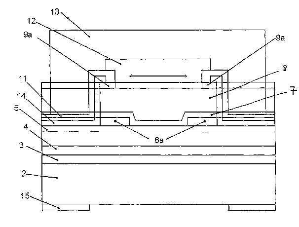
Finally, Figure 7 shows the structure of the finished
semiconductor laser according to the invention with wave
guiding (WG-VCSEL); the processing of this structure on
the basis of those shown in Figures 5 and 6 corresponds
to the technology known from the BTJ-VCSELs, which was
discussed at length in the introduction to the
description. Therefore, no detailed description will be
provided at this point. In the finished WG-VCSEL the
original n-InP substrate 1 has been totally removed and
an n-end contact 15 has been fitted. On the n-doped
confinement layer 8 is an annular p-end contact layer 9a,
which encloses a dielectric mirror 12. The p-end contact
11 (e. g. Au/Ti/Pt/Au) is separated from the n-doped
confinement layer 8 by an insulating and passivating
layer 14 (e.g. consisting of Si3N4 or A1203) . On this
structure is the surrounding integrated gold heat sink
13. The n-end contact 15 consists of Ti/Pt, for example.
The laser light emerges from the semiconductor laser on
its side.
CA 02514134 2005-07-22
- 16 -
Finally, it should be pointed out that the active zone 3
which is shown here as a homogeneous layer usually
consists of a layer structure of for example 11 thin
layers (5 quantum film and 6 barrier layers).
The invention makes it possible to manufacture a VCSEL
with waveguide structure having a continuously adjustable
range of lateral wave guiding and mode selection. The
single mode performance (output) is increased compared
with previously known laser diodes.