Note: Descriptions are shown in the official language in which they were submitted.
CA 02514265 2005-07-25
WO 2004/067806 PCT/GB2004/000318
1
STENCIL MANUFACTURE
The present invention relates to a method for making
a stencil for use in screen-printing.
Screen printing stencils define a pattern with open
areas on the stencil. A material is printed through the
open areas of the stencil, so that the printed deposits
match approximately those open areas. Screen-printing
stencils have a number of uses in the electronic
substrate fabrication and electronic assembly industries.
These include, but are not limited to the printing of
printed circuit boards, depositing solder paste and
conductive adhesive for electronic packaging and the
printing of conductor and resistor circuits.
The drive to make electronic devices smaller, faster
and lighter, but at the same time with higher pin counts,
has lead to a trend of using advanced packaging
techniques,' which eliminate the use of leads for
interconnects. Using advanced packaging technique s
enables an increase in the number of connections and a
decrease in package size, and so an increase in package
performance and a drop in production cost. One of the
fastest and most cost attractive options to package
electronic components is to screen print the interconnect
material through the apertures of a stencil and then
package the components accordingly. However, currently
there are practical limitations. This is because known
processes for making stencils do not allow the
fabrication of stencils with perfect apertures at a fine
pitch. For small features (e.g. sub 100 micron), it is
critical that the stencil apertures are perfectly formed,
with high tolerances to enable the same paste volume to
be effectively released from each aperture and printed.
Conventional metal stencils can be fabricated in
various ways. In a first known method chemical etching
CA 02514265 2005-07-25
WO 2004/067806 PCT/GB2004/000318
2
is used. This involves firstly forming a resist mask by
applying a resist to a metal foil and optically
patterning the resist through a mask. The resist is then
developed leaving the pattern of the mask on the foil.
The foil with its resist mask is then submerged in a
chemical etchant. The areas covered by the resist mask
are protected and stop the metal foil being etched away.
In contrast, the exposed areas not covered by the resist
mask are etched away, thereby forming apertures through
the metal foil and so defining a stencil. A disadvantage
of chemical etched stencils is that they cannot be
reliably manufactured with small apertures and fine pitch
due to the undercutting process caused by etching. This
can cause problems when the stencil is used, because
paste can get trapped in the undercut sidewall.
Therefore, such stencils~are only used for larger pitch
features.
In another method laser cutting is used. This
involves mounting a metal foil in a frame. Stored in a
computer is a data file that represents an image of the
apertures that are required to form the desired stencil.
Under control of the computer, a laser traces out this
image ablating each aperture sequentially. However, the
laser cutting process for the formation of screen-
printing stencils also has some drawbacks for forming
fine pitch apertures. Notably the laser cuts rough
aperture walls, which can cause paste or adhesive to get
trapped in the apertures during printing. Another
problem is that the process can be quite messy at fine
pitches, spewing molten metal around the aperture and
often causing an undesirable lip around the edge of some
apertures. Furthermore, incomplete removal of metal can
occur leaving blocked apertures. Another problem is that
CA 02514265 2005-07-25
WO 2004/067806 PCT/GB2004/000318
3
the diameter of apertures can vary by +/- 10 microns at
fine pitches.
Yet another method for manufacturing stencils uses
DC electroforming. This process starts with a properly
prepared mandrel, typically a stainless steel sheet,
which is laminated with a dry film photo resist. The
resist is exposed to a collimated UV light source through
a mask, and then developed, leaving a pattern of the
apertures. Once this is done, the patterned mandrel~is
submerged in a suitable electroplating solution and
exposed to a high DC electrical current, which starts the
plating process. Metal ions are deposited around the
photo resist to the desired stencil thickness. The next
step is to strip away the polymerised photo resist and
then mechanically remove the foil. An example of a DC
electroforming process is described in US 5,359,928.
A problem with DC electroforming technology is that
it cannot reliably produce a stencil at sub-150 micron
pitches. Hence at these levels, the aperture shape and
size vary from one to another. Also, traditional DC
electroforming does not plate uniformly across a
substrate due to current crowding effects. This uneven
current density causes an uneven plating rate and hence
an overall variation of plated metal across the stencil.
It also tends to cause a gasket or lip around the
aperture, which can cause bleeding during the printing
process.
An object of the invention is to provide an improved
method for fabricating stencils and an improved
resolution stencil.
According to one aspect of the present invention
there is provided a method of forming a stencil
comprising electroforming the stencil using a bi-polar
CA 02514265 2005-07-25
WO 2004/067806 PCT/GB2004/000318
4
electrical signal that comprises a plurality of bi-polar
waveforms.
Using bi-polar electroforming has several inherent
advantages over traditional DC electroforming. Most
notably, it allows the material distribution to be
controlled thereby to give an even metal deposition
across the stencil, which means that the edge definition
of features formed using this method is excellent. Also,
material properties can be controlled, for example,
hardness, intrinsic stress, brittleness, ductility, and
crystal structure. Furthermore, the current efficiency is
improved, which decreases hydrogen formation, thus
lowering pitting and decreasing residual stress. In
addition, in practice, using this method reduces or
eliminates the need for organic additives.
By bi-polar waveform, it is meant a waveform
consisting of a positive pulse and a negative pulse.
When the positive pulse of the bi-polar waveform is
applied during the electroforming -process, metal is
deposited. This positive pulse will be referred to as
the cathodic pulse. When the negative pulse is applied;
metal is removed. This negative pulse will be referred
to as the anodic pulse.
Preferably, the cathodic pulse has a longer duration
than the anodic pulse. Preferably, the cathodic pulse is
at least twice the duration of the anodic pulse. The
ratio of cathodic pulse duration to anodic pulse duration
may be in the range of 2:1 to 100:1.
Preferably, the cathodic pulse has a lower peak
value than the anodic pulse. The ratio of cathodic pulse
height to anodic pulse height may be in the range of
about 1:1.5 to 1:20. The anodic pulse height may be
substantially 1.5 times the cathodic pulse height. The
CA 02514265 2005-07-25
WO 2004/067806 PCT/GB2004/000318
anodic pulse height may be substantially 20 times the
cathodic pulse height.
The method may involve varying the bi-polar
waveforms. For example, initially a bi-polar waveform
5 that is suitable to provide smooth stencil sidewalls may
be used, and subsequently, towards the end of the
process, the waveform may be varied in order to provide a
rough upper surface. This may be done by varying the
frequency and/or the durations of the cathodic and ano.dic
pulses and/or the magnitudes of the eathodic and anodic
pulses and/or the relative widths of the cathodic and
anodic pulses and/or the relative magnitudes of the
cathodic and/or anodic pulses.
The waveform may be square or spiked or sinusoidal.
In general it is preferred that bi-polar waveform is
a current waveform. In this case, the voltage is
controlled and it is the current that is varied. Of
course, the bi-polar waveform could equally be a voltage.
waveform. In this case, the voltage. waveform is varied
with respect to current.
Where the bi-polar waveform is a current waveform,
it may have a pulse width in the millisecond range 1ms-
999ms. In this case, the voltage range depends on the
size of the substrate.
The average current density of the anodic pulse is
less than the average current density of the cathodic
waveform.
The current may have a peak density in the range of
from 1Am/dm2 to 50A/dm~, where A/dm2 - Amps per decimeter
squared and a decimeter is 100cm2.
The average current density may be in the range 3-
15A/dm~, where the average current density is an average
of the current across one waveform.
CA 02514265 2005-07-25
WO 2004/067806 PCT/GB2004/000318
6
The step of electroforming the stencil may comprise
providing a mould on a conducting surface, the mould
defining exposed areas of the conducting surface;
immersing the mould and conducting surface in an ionic
solution and electroplating areas exposed by the mould
using the bi-polar current or voltage~signal.
The mould may be provided on an intermediary layer
that is carried by the conducting surface. The
intermediary layer may be a sacrificial lift-off layer
for allowing easy removal of the stencil from the
substrate.
According to another aspect of the present invention
there is provided a system for forming a stencil
comprising a mask on a conducting surface, the mask
defining exposed areas of the conducting surface, and
means for electroplating areas exposed by the mask using
a bi-polar current or voltage signal that comprises a
plurality of waveforms each having a catholic pulse and a
anodic pulse.
Preferably, the catholic pulse has a longer duration
than the anodic pulse. Preferably, the catholic pulse is
at least twice the duration of the anodic pulse. The
ratio of catholic pulse duration to anodic pulse duration
may be in the range of 2:1 to 100:1.
Preferably, the catholic pulse has a lower peak
value than the anodic pulse. The ratio of catholic pulse
height to anodic pulse height may be in the range of
about 1:1.5 to 1:20. The anodic pulse height may be
substantially 1.5 times the catholic pulse height. The
anodic pulse height may be substantially twenty times the
catholic pulse height.
The bi-polar waveform preferably has a greater
anodic to catholic pulse ratio, and a shorter anodic
pulse time than catholic pulse time.
CA 02514265 2005-07-25
WO 2004/067806 PCT/GB2004/000318
7
The waveform may be square or spiked or sinusoidal.
The bi-polar waveform may be a current waveform.
Alternatively, the bi-polar waveform could be a voltage
waveform.
When the bi-polar waveform is a current waveform,
the average current density of the anodic pulse is
preferably less than the average current density of the
cathodic waveform.
When the bi-polar waveform is a current waveform,
the average current density may be in the range 3-10A/dm2.
The waveform may have an average current density of
7A/dm~, a frequency of ~OHz(50ms), a cathodic pulse
duration of 45ms at 10A/dm2, and an anodic pulse duration
of 5ms at 20A/dm2.
When the bi-polar waveform is a current waveform, it
may have a pulse width in the millisecond range 1ms-
999ms. In this case, the voltage range depends on the
size of the wafer.
When the bi-polar waveform is a current waveform,
the current may have a peak density in the range of
anywhere from 1Am/dm2 to 50A/dm~, where A/dm2 - Amps per
decimeter squared and a decimeter is 100cm2.
A controller may be provided for controlling
parameters of the bi-polar signal. The controller may be
~5 operable to vary parameters of the bi-polar signal at
different stages in the electroforming process. The
parameters may be the frequency and/or the durations of
the cathodic and anodic pulses and/or the magnitudes of
the cathodic and anodic pulse and/or the relative widths
of the cathodic and anodic pulses and/or the relative
magnitudes of the cathodic and/or anodic pulses.
By varying the signal parameters at different stages
in the electroforming process, the physical
characteristics of the stencil can be caused to be
CA 02514265 2005-07-25
WO 2004/067806 PCT/GB2004/000318
8
different in different areas thereof. This means that in
the early stages of the process, the pulse can be
controlled so as to provide very smooth sidewall
definition, but at the latter stages, once plating is
substantially finished, the parameters could be changed
so that the stencil has a rough upper surface. Providing
a rough upper surface aids in the printing process,
z
because it improves rolling of the paste onto the
stencil. Having smooth sidewalls aids printing, because
it encourages better material release from the apertures.
According to yet another aspect of the present
invention there is provided a method comprising: forming
a stencil by providing a mould on a conducting surface,
the mould defining exposed areas of the conducting
surface; electroplating the exposed areas of the
conducting surface using a bi-polar current or voltage
signal, thereby to form a stencil and using the stencil
to print features onto a board or substrate or some other
suitable medium.
Various aspects of the invention will now be
described by way of example only with reference to the
accompanying drawing, of which:
Figure 1 is a perspective view of a substrate for
use in forming a stencil;
Figure 2 is a perspective view of the. substrate of
Figure 1, on which resist is deposited;
Figure 3 is a perspective view of the substrate of
Figure 2, to which a mask is applied;
Figure 4 is a perspective view of the substrate of
Figure 3 after patterning and development of the resist;
Figure 5 is a schematic representation of a system
for electroforming a stencil;
Figure 6 is a perspective view of an electroformed
stencil on the substrate;
CA 02514265 2005-07-25
WO 2004/067806 PCT/GB2004/000318
9
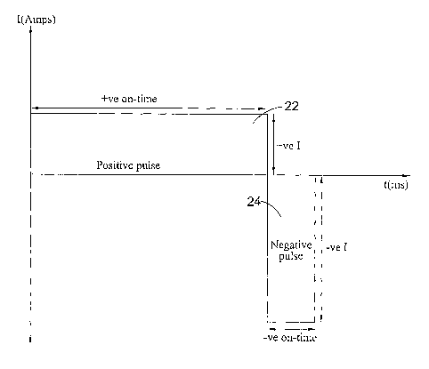
Figure 7 shows an example of a bi-polar pulse
applied during the electroplating process;
Figure 8 is a perspective view of the stencil of
Figure 7, after removal from the substrate, and
Figure 9 is a perspective view of the final stencil.
The starting material in the stencil forming process
is a substrate 10 of, for example, glass, as shown in
Figure 1. Of course any other suitable substrate could
be used, for example a dielectric material such as
silicon or ceramic. The substrate 10 is cleaned using
any suitable method, for example, successive immersions
in methanol, acetone and piranha solution and then de-
ionised water. A conductive seed layer of metal 12 is
then deposited on an upper surface of the glass wafer 10.
This can be done using an electron beam evaporator or any
other suitable technique, such as sputtering or thermal
evaporation. The metal 12 must have a thickness that is
sufficient to allow it to conduct. The thickness may be
in the range of 0.1 to 0.3 microns.
A variety of metals can be used for the seed layer
12 either alone or as part of a bi-metallic or tri-
metallic layered structure. However, as an example,
titanium could be used, as could a
titanium/copper/titanium layered structure or a
chrome/copper/gold layered structure. V~lhen~using a glass
substrate it is preferred that the base metal layer is
titanium or chrome. This is because these metals promote
adhesion to the substrate. As an alternative, rather
than using a glass substrate that is coated with metal, a
metal substrate could be used.
Once the metal layer 12 is formed, photoresist 14 is
deposited on it, as shown in Figure 2. Any suitable
photoresist 14 could be used, but a preferred example is
SU-8. As is well known, this is a negative resist. The
CA 02514265 2005-07-25
WO 2004/067806 PCT/GB2004/000318
photoresist 14 can be deposited in any suitable manner,
for example spin coating. In order to give a photoresist
thickness of approximately 50 microns the spin speed may
be around 3000 revs per minute. Of course, this could be
5 varied according to the thickness of the stencil
required. Alternatively, the resist could be applied as
a film or using a doctor blading machine, also known as a
knife coater. The resist covered glass wafer/substrate is
than baked at a temperature in the range of 50-130°C, for
10 example 90°C, on a hot plate or oven for between one
minute and two hours. As will be appreciated, the
absolute temperature and time here depend on the
thickness of the photoresist. The thicker the
photo-resist 14 the longer it takes to bake.
After the photoresist 14 is baked, it is patterned
through a photomask 16 using photolithography, as shown
in Figure 3. The photomask is a chrome-on-glass mask,
although a mask made on a high-resolution photoplotter
could also be used. The resist 14 is exposed through the
mask 16 using a highly collimated light source having a
suitable wavelength. For SU-8, the wavelength is
typically in a range of about 350nm to 400nm, preferably
365nm. The energy of the light used is in the range of
100-5000 mJ/cm2. However, it will be appreciated that
the wavelength and energy used will depend on the
sensitivity of the resist. The patterned resist 14 is
then baked using, for example, a hotplate or an oven.
The baking temperature is in the range 50-130°C,
preferably 90°C. The duration of baking is dependant on
the photoresist thickness but may be anywhere between 1
minute and 2 hours. Of course, it will be appreciated
that this post-patterning bake may not be necessary for
other types of resist.
CA 02514265 2005-07-25
WO 2004/067806 PCT/GB2004/000318
11
After baking, the photoresist 14 is developed in
Microposit EC Solvent or acetone or any other suitable
solvent. Development can be done by complete immersion
in the solution, with some agitation thereof, or by
spraying the solution onto the surface. Using Microposit
EC Solvent, the time taken to develop the resist is of
the order of 2 to 3 minutes, although it will be
appreciated that this time will vary depending on the
developing chemical used. Once the resist is developed,
mesas 18 of resist in the areas that were exposed remain,
and all of the other resist is removed. These patterned
resist mesas 18 define the aperture shapes for the
stencil, as shown in Figure 4.
Once the mesas 18 are formed, the electroforming
process is implemented. Figure 5 shows a system that is
suitable for this. This includes a variable current
source that is operable to output a bi-polar current
signal; an anode and a bath for the electroplating
solution. Electroplating can be done using any suitable
solution, but a preferred option is a solution made with
nickel sulphamate (3308 per litre), boric acid (30g per
litre) and nickel chloride (15g per litre). In this
case, a 99.990 pure nickel anode is used. The solution
should be at 50°C. The wafer is submerged in the
solution in the plating bath. Once this is done, an AC
bi-polar current is applied between the conductive seed
layer 12 and the anode. This causes the formation of the
stencil, as shown in Figure 6.
Figure 7 shows an example of the bi-polar AC current
waveform used. Preferably, the bi-polar signal includes
a continuous stream of these waveforms, although off
times, during which no current is applied, could be used
if and when desired. The waveform of Figure 7 is square
and consists of a cathodic pulse 22 and an anodic pulse
CA 02514265 2005-07-25
WO 2004/067806 PCT/GB2004/000318
12
24. By cathodic pulse, it is meant that part of the bi-
polar waveform that causes deposition of metal. By anodic
pulse, it is meant that part of the bi-polar waveform
that causes removal of metal. In the case of the waveform
shown in Figure 7, the cathodic pulse is represented by
the positive pulse 22 and the anodic pulse is represented
by the negative pulse 24.
The cathodic pulse 22 has a longer duration,
preferably at least double, than the anodic pulse 24 'and
has a lower peak forward current . The anodic pulse 24 is
much shorter, but has a relatively high peak current.
The average current density of the cathodic pulse 22 is
greater than that of the anodic pulse 24.
The bi-polar AC current waveform used is typically
in the millisecond range lms-999ms, with a greater anodic
to cathodic pulse ratio, and a shorter anodic pulse time
than cathodic pulse time. The voltage range depends on
the size of the wafer. For example, for an eight-inch
wafer, the voltage used was 12V, but between 1 to 100
volts is possible. It should be noted that in general it
is preferred that voltage is controlled and it is the
current that is varied, although of course, it is
possible also to vary the voltage waveform with respect
to current. The current typically ranges anywhere from
1Am/dm~ to 50A/dm2, where A/dm2 - Amps per decimeter
squared. The average current density is usually from 3-
10A/dm2. A typical waveform for plating pure nickel has
an average current density of 7A/dm2, a frequency of
20Hz (50ms) , a cathodic pulse duration of 45ms at 10A/dm~,
and an anodic pulse duration of 5ms at 20A/dm2.
Once the desired thickness of the material has been
reached, the electroplating process is stopped and the
wafer with its electro-formed stencil 20 is removed from
the solution. The stencil 20 is then removed from the
CA 02514265 2005-07-25
WO 2004/067806 PCT/GB2004/000318
13
substrate 10. This can be done by merely peeling the
stencil 20 off the wafer/substrate. At this stage, the
resist mesas 18 infill the apertures, as shown in Figure
8. The resist is removed using a suitable solvent,
thereby leaving the stencil 20, as shown in Figure 9.
For SU-8 the preferred solvent is MS111, which is
available from Miller Stephens Corporation, USA. The
stencil 20 is then cleaned to remove any residual MS-111
and SU-8. This can be done by blowing dry the stencil~in
nitrogen. The stencil is then mounted in a frame (not
shown) using conventional mounting techniques, so that it
can then be used for printing in the electronic substrate
fabrication and electronic assembly line industries.
Using a bi-polar AC current to electroform a metal
stencil provides good metal deposition uniformity, and
allows very fine features to be defined. By varying the
pulse parameters, it is possible to control the material
properties of the stencil, such as the hardness and
surface roughness. This is because, by controlling the
waveform parameters, it is possible to alter deposition
of the stencil at an atomic level. The pulse parameters
that can be varied include the frequency and/or relative
widths of the cathodic and anodic pulses and/or relative
heights of the cathodic and anodic pulses. In practice,
it has been found that at higher frequencies surface
smoothness is improved, whereas at lower frequencies,
surface roughness is increased. As an example, for the
specific stencil forming process described above, it was
found that using a frequency of 100Hz provided a smooth
surface, whereas using 4Hz or DC produced a rougher
surface. Hence, by varying the frequency surface
properties can be varied.
The bi-polar electro-forming stencil manufacture
technique in which the invention is embodied provides
CA 02514265 2005-07-25
WO 2004/067806 PCT/GB2004/000318
14
various advantages. For example, in contrast to
conventional DC techniques, when bi-polar pulses are
used, the electroplating process does not require the use
of organic additives in the electroplating bath. These
additives are costly and difficult to maintain, and
removing them from the process lessens the need for
monitoring equipment to monitor the additive mixes. The
method also provides a very even distribution of metal
across the stencil. In addition, it provides a mechanism
for controlling material properties, such as hardness,
intrinsic stress and crystal structure. This enables the
possibility of providing a rough upper surface for the
stencil to aid printing but at the same time providing
very smooth sidewalls in order to perfectly release
paste. Furthermore, the current efficiency is improved,
which decreases hydrogen formation, thus lowering pitting
and decreasing residual stress.
A skilled person will appreciate that variations of
the disclosed arrangements are possible without departing
from the invention. For example, whilst the stencil is
described as being formed using a negative photo-resist,
a positive resist could equally be used. In addition,
although the stencil is described above as being peeled
away from the substrate other options are possible. For
example, the mould may be provided on an~ intermediary
layer that is carried by the conducting surface. The
intermediary layer may be a sacrificial lift-off layer
that can be dissolved away, thereby to allow easy removal
of the stencil from the substrate. The sacrificial lift
off layer (not shown) could be deposited between the
metal seed layer and the stencil layer. Alternatively, a
sacrificial substrate that can be dissolved away could
also be used. Furthermore, whilst the waveforms
described above are all square, spike waveforms and
CA 02514265 2005-07-25
WO 2004/067806 PCT/GB2004/000318
sinusoidal waveforms are also suitable. Accordingly, the
above description of a specific embodiment is made by way
of example only and not for the purposes of limitation.
It will be clear to the skilled person that minor
5 modifications may be made without significant changes to
the operation described.