Note: Descriptions are shown in the official language in which they were submitted.
CA 02514349 2005-08-17
Internal reference: IRDM.096 NON-EP / IDC-40058
METHOD OF SELECTIVE ETCHING USING ETCH STOP LAYER
Back round
Field of the Invention
The field of the invention relates to microelectromechanical systems (MEMS).
Description of the Related Technoloay
Microelectromechanical systems (MEMS) include micro mechanical elements,
actuators,
and electronics. Micromechanical elements may be created using deposition,
etching, and or
other micromachining processes that etch away parts of substrates and/or
deposited material
layers or that add layers to form electrical and electromechanical devices.
One type of MEMS
device is called an interferometric modulator. An interferometric modulator
may comprise a pair
of conductive plates, one or both of which may be transparent and/or
reflective in whole or part
and capable of relative motion upon application of an appropriate electrical
signal. One plate
may comprise a stationary layer deposited on a substrate, the other plate may
comprise a metallic
membrane separated from the stationary layer by a gap. Such devices have a
wide range of
applications, and it would be beneficial in the art to utilize and/or modify
the characteristics of
these types of devices so that their features can be exploited in improving
existing products and
creating new products that have not yet been developed.
Summary
The systems, methods, and devices described herein each have several aspects,
no single
one of which is solely responsible for its desirable attributes. Without
limiting the scope of this
invention, its more prominent features will now be discussed briefly. After
considering this
discussion, and particularly after reading the section entitled "Detailed
Description of the
Preferred Embodiments" one will understand how the various embodiments
described herein
provide advantages over other methods and display devices.
An aspect provides an unreleased interferometric modulator that includes a
sacrificial
layer, a metal mirror layer over the sacrificial layer, and an etch stop layer
between the sacrificial
layer and the metal mirror layer. In an embodiment, the sacrificial layer
includes amorphous
silicon, germanium and/or molybdenum. In an embodiment, the etch stop layer
includes a silicon
oxide, amorphous silicon, a silicon nitride, germanium, titanium, and/or
tungsten. In any
particular interferometric modulator, the material used to form the
sacrificial layer is generally
different than the material used to form the etch stop layer.
CA 02514349 2005-08-17
An aspect provides a method of making an interferometric modulator that
includes
depositing a sacrificial layer over a first mirror layer, depositing an etch
stop layer over the
sacrificial layer, and depositing a second mirror layer over the etch stop
layer. A portion of the
second mirror layer is then removed to expose the etch stop layer, thereby
forming an exposed
portion of the etch stop layer and an unexposed portion of the etch stop
layer. The unexposed
portion of the etch stop layer underlies a remaining portion of the second
mirror layer. Various
embodiments provide interferometric modulators (including unreleased
interferometric
modulators) made by such a method.
Another aspect provides a method of making an interferometric modulator that
includes
depositing a sacrificial layer over a first mirror layer, depositing an etch
stop layer over the
sacrificial layer, depositing a second mirror layer over the etch stop layer,
and removing the
sacrificial layer to expose a portion of the etch stop layer underlying the
second mirror layer. In
an embodiment, the sacrificial layer is removed using an etchant that removes
the sacrificial layer
at a rate that is at least about 5 times faster than a rate at which the
etchant removes the etch stop
layer.
Another aspect provides a method of making an interferometric modulator that
includes
depositing a sacrificial layer over a first mirror layer. The sacrificial
layer includes amorphous
silicon, germanium and/or molybdenum. The method further includes depositing
an etch stop
layer over the sacrificial layer. The etch stop layer includes a silicon
oxide, amorphous silicon, a
silicon nitride, germanium, titanium, and/or tungsten. In any particular
process flow, the
material used to form the sacrificial layer is generally different than the
material used to form the
etch stop layer. The method further includes depositing a second mirror layer
over the etch stop
layer. The second mirror layer includes a metal such as Al, Al-Si, Al-Cu, Al-
Ti, and/or Al-Nd.
The method further includes removing a portion of the second mirror layer to
expose the etch
stop layer, thereby forming an exposed portion of the etch stop layer and an
unexposed portion of
the etch stop layer. The unexposed portion of the etch stop layer underlies a
remaining portion of
the second mirror layer. The method further includes removing the sacrificial
layer to expose the
previously unexposed portion of the etch stop layer underlying the remaining
portion of the
second mirror layer.
These and other aspects will be better understood from the embodiments
described in
greater detail below.
-2-
CA 02514349 2005-08-17
Brief Description of the Drawings
These and other features of this invention will now be described with
reference to the
drawings of preferred embodiments (not to scale) which are intended to
illustrate and not to limit
the invention.
Figure 1 is an isometric view depicting a portion of one embodiment of an
interferometric modulator display in which a movable reflective layer of a
first interferometric
modulator is in a relaxed position and a movable reflective layer of a second
interferometric
modulator is in an actuated position.
Figure 2 is a system block diagram illustrating one embodiment of an
electronic device
incorporating a 3x3 interferometric modulator display.
Figure 3 is a diagram of movable mirror position versus applied voltage for
one
exemplary embodiment of an interferometric modulator of Figure 1.
Figure 4 is an illustration of a set of row and column voltages that may be
used to drive
an interferometric modulator display.
Figures SA and SB illustrate one exemplary timing diagram for row and column
signals
that may be used to write a frame of display data to the 3x3 interferometric
modulator display of
Figure 2.
Figure 6A is a cross section of the device of Figure 1.
Figure 6B is a cross section of an alternative embodiment of an
interferometric modulator.
Figure 6C is a cross section of another alternative embodiment of an
interferometric
modulator.
Figure 7 is a cross-sectional view showing an embodiment of an unreleased
interferometric modulator.
Figures 8A-8E are cross-sectional views illustrating the initial process steps
in an
embodiment of a method for making an array of interferometric modulators.
Figures 9A-9H are cross-sectional views illustrating the later process steps
in the
embodiment of a method for making an array of interferometric modulators.
Detailed Description of the Preferred Embodiments
An embodiment provides a method for making an interferometric modulator that
involves
the use of an etch stop between the upper mirror layer and the sacrificial
layer. Both unreleased
and released interferometric modulators may be fabricated using this method.
The etch stop can
be used to reduce undesirable over-etching of the sacrificial layer and the
upper mirror layer.
The etch stop layer may also serve as a barrier layer, buffer layer, and/or
template layer.
The following detailed description is directed to certain specific embodiments
of the
invention. However, the invention can be embodied in a multitude of different
ways. In this
-3-
CA 02514349 2005-08-17
description, reference is made to the drawings wherein like parts are
designated with like
numerals throughout. As will be apparent from the following description, the
embodiments may
be implemented in any device that is configured to display an image, whether
in motion (e.g.,
video) or stationary (e.g., still image), and whether textual or pictorial,
and/or processes for
making such devices. More particularly, it is contemplated that the
embodiments may be
implemented in or associated with a variety of electronic devices such as, but
not limited to,
mobile telephones, wireless devices, personal data assistants (PDAs), hand-
held or portable
computers, GPS receivers/navigators, cameras, MP3 players, camcorders, game
consoles, wrist
watches, clocks, calculators, television monitors, flat panel displays,
computer monitors, auto
displays (e.g., odometer display, etc.), cockpit controls and/or displays,
display of camera views
(e.g., display of a rear view camera in a vehicle), electronic photographs,
electronic billboards or
signs, projectors, architectural structures, packaging, and aesthetic
structures (e.g., display of
images on a piece of jewelry). MEMS devices of similar structure to those
described herein can
also be used in non-display applications such as in electronic switching
devices.
One interferometric modulator display embodiment comprising an interferometric
MEMS display element is illustrated in Figure 1. In these devices, the pixels
are in either a
bright or dark state. In the bright ("on" or "open") state, the display
element reflects a large
portion of incident visible light to a user. When in the dark ("ofF' or
"closed") state, the display
element reflects little incident visible light to the user. Depending on the
embodiment, the light
reflectance properties of the "on" and "off' states may be reversed. MEMS
pixels can be
configured to reflect predominantly at selected colors, allowing for a color
display in addition to
black and white.
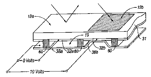
Figure 1 is an isometric view depicting two adjacent pixels in a series of
pixels of a
visual display, wherein each pixel comprises a MEMS interferometric modulator.
In some
embodiments, an interferometric modulator display comprises a row/column array
of these
interferometric modulators. Each interferometric modulator includes a pair of
reflective layers
positioned at a variable and controllable distance from each other to form a
resonant optical
cavity with at least one variable dimension. In one embodiment, one of the
reflective layers may
be moved between two positions. In the first position, referred to herein as
the relaxed state, the
movable layer is positioned at a relatively large distance from a fixed
partially reflective layer. In
the second position, the movable layer is positioned more closely adjacent to
the partially
reflective layer. Incident light that reflects from the two layers interferes
constructively or
destructively depending on the position of the movable reflective layer,
producing either an
overall reflective or non-reflective state for each pixel.
The depicted portion of the pixel array in Figure 1 includes two adjacent
interferometric
modulators 12a and 12b. In the interferometric modulator 12a on the left, a
movable and highly
-4-
CA 02514349 2005-08-17
reflective layer 38a is illustrated in a relaxed position at a predetermined
distance from a fixed
partially reflective layer 32a. In the interferometric modulator 12b on the
right, the movable
highly reflective layer 38b is illustrated in an actuated position adjacent to
the fixed partially
reflective layer 32b.
The fixed layers 32a, 32b are electrically conductive, partially transparent
and partially
reflective, and may be fabricated, for example, by depositing one or more
layers each of
chromium and indium-tin-oxide onto a transparent substrate 31. The layers are
patterned into
parallel strips, and may form row electrodes in a display device as described
further below. The
movable layers 38a, 38b may be formed as a series of parallel strips of a
deposited metal layer or
layers (orthogonal to the row electrodes 32a, 32b) deposited on top of posts
60 and an
intervening sacrificial material deposited between the posts 60. When the
sacrificial material is
etched away, the deformable metal layers 38a, 38b are separated from the fixed
conductive/partially reflective metal layers 32a, 32b by a defined gap 19. A
highly conductive
and reflective material such as aluminum may be used for the deformable
layers, and these strips
may form column electrodes in a display device.
With no applied voltage, the cavity 19 remains between the layers 38a, 32a and
the
deformable layer is in a mechanically relaxed state as illustrated by the
pixel 12a in Figure 1.
However, when a potential difference is applied to a selected row and column,
the capacitor
formed at the intersection of the row and column electrodes at the
corresponding pixel becomes
charged, and electrostatic forces pull the electrodes together. If the voltage
is high enough, the
movable layer is deformed and is forced against the fixed layer (a dielectric
material which is not
illustrated in this Figure may be deposited on the fixed layer 32a, 32b to
prevent shorting and
control the separation distance) as illustrated by the pixel 12b on the right
in Figure 1. The
behavior is the same regardless of the polarity of the applied potential
difference. In this way,
row/column actuation that can control the reflective vs. non-reflective pixel
states is analogous in
many ways to that used in conventional LCD and other display technologies.
Figures 2 through 5 illustrate one exemplary process and system for using an
array of
interferometric modulators in a display application. Figure 2 is a system
block diagram
illustrating one embodiment of an electronic device that may incorporate
aspects of the invention.
In the exemplary embodiment, the electronic device includes a processor 21
which may be any
general purpose single- or multi-chip microprocessor such as an ARM, Pentium~,
Pentium II~,
Pentium III~, Pentium IV~, Pentium Pro, an 8051, a MIPS~, a Power PC~, an
ALPHA~, or any
special purpose microprocessor such as a digital signal processor,
microcontroller, or a
programmable gate array. As is conventional in the art, the processor 21 may
be configured to
execute one or more software modules. In addition to executing an operating
system, the
-5-
CA 02514349 2005-08-17
processor may be configured to execute one or more software applications,
including a web
browser, a telephone application, an email program, or any other software
application.
In one embodiment, the processor 21 is also configured to communicate with an
array
controller 22. In one embodiment, the array controller 22 includes a row
driver circuit 24 and a
column driver circuit 26 that provide signals to a pixel array 30. The cross
section of the array
illustrated in Figure 1 is shown by the lines 1-1 in Figure 2. For MEMS
interferometric
modulators, the row/column actuation protocol may take advantage of a
hysteresis property of
these devices illustrated in Figure 3. It may require, for example, a 10 volt
potential difference to
cause a movable layer to deform from the relaxed state to the actuated state.
However, when the
voltage is reduced from that value, the movable layer maintains its state as
the voltage drops back
below 10 volts. In the exemplary embodiment of Figure 3, the movable layer
does not relax
completely until the voltage drops below 2 volts. There is thus a range of
voltage, about 3 to 7 V
in the example illustrated in Figure 3, where there exists a window of applied
voltage within
which the device is stable in either the relaxed or actuated state. This is
referred to herein as the
"hysteresis window" or "stability window." For a display array having the
hysteresis
characteristics of Figure 3, the row/column actuation protocol can be designed
such that during
row strobing, pixels in the strobed row that are to be actuated are exposed to
a voltage difference
of about 10 volts, and pixels that are to be relaxed are exposed to a voltage
difference of close to
zero volts. After the strobe, the pixels are exposed to a steady state voltage
difference of about 5
volts such that they remain in whatever state in which the row strobe put
them. After being
written, each pixel sees a potential difference within the "stability window"
of 3-7 volts in this
example. This feature makes the pixel design illustrated in Figure 1 stable
under the same
applied voltage conditions in either an actuated or relaxed pre-existing
state. Since each pixel of
the interferometric modulator, whether in the actuated or relaxed state, is
essentially a capacitor
formed by the fixed and moving reflective layers, this stable state can be
held at a voltage within
the hysteresis window with almost no power dissipation. Essentially no current
flows into the
pixel if the applied potential is fixed.
In typical applications, a display frame may be created by asserting the set
of column
electrodes in accordance with the desired set of actuated pixels in the first
row. A row pulse is
then applied to the row 1 electrode, actuating the pixels corresponding to the
asserted column
lines. The asserted set of column electrodes is then changed to correspond to
the desired set of
actuated pixels in the second row. A pulse is then applied to the row 2
electrode, actuating the
appropriate pixels in row 2 in accordance with the asserted column electrodes.
The row 1 pixels
are unaffected by the row 2 pulse, and remain in the state they were set to
during the row 1 pulse.
This may be repeated for the entire series of rows in a sequential fashion to
produce the frame.
Generally, the frames are refreshed and/or updated with new display data by
continually
-6-
CA 02514349 2005-08-17
repeating this process at some desired number of frames per second. A wide
variety of protocols
for driving row and column electrodes of pixel arrays to produce display
frames are also well
known and may be used in conjunction with the present invention.
Figures 4 and 5 illustrate one possible actuation protocol for creating a
display frame on
the 3x3 array of Figure 2. Figure 4 illustrates a possible set of column and
row voltage levels that
may be used for pixels exhibiting the hysteresis curves of Figure 3. In the
Figure 4 embodiment,
actuating a pixel involves setting the appropriate column to -Vb;as, and the
appropriate row to
+0V, which may correspond to -5 volts and +5 volts respectively Releasing the
pixel is
accomplished by setting the appropriate column to +Vb;es, and the appropriate
row to the same
+~V, producing a zero volt potential difference across the pixel. In those
rows where the row
voltage is held at zero volts, the pixels are stable in whatever state they
were originally in,
regardless of whether the column is at +Vb;~, or -Vb;~.
Figure SB is a timing diagram showing a series of row and column signals
applied to the
3x3 array of Figure 2 which will result in the display arrangement illustrated
in Figure SA, where
actuated pixels are non-reflective. Prior to writing the frame illustrated in
Figure SA, the pixels
can be in any state, and in this example, all the rows are at 0 volts, and all
the columns are at +5
volts. With these applied voltages, all pixels are stable in their existing
actuated or relaxed states.
In the Figure SA frame, pixels (1,1), (1,2), (2,2), (3,2) and (3,3) are
actuated. To
accomplish this, during a "line time" for row 1, columns 1 and 2 are set to -5
volts, and column 3
is set to +5 volts. This does not change the state of any pixels, because all
the pixels remain in
the 3-7 volt stability window. Row 1 is then strobed with a pulse that goes
from 0, up to 5 volts,
and back to zero. This actuates the (1,1) and (1,2) pixels and relaxes the
(1,3) pixel. No other
pixels in the array are affected. To set row 2 as desired, column 2 is set to -
S volts, and columns
1 and 3 are set to +5 volts. The same strobe applied to row 2 will then
actuate pixel (2,2) and
relax pixels (2,1) and (2,3). Again, no other pixels of the array are
affected. Row 3 is similarly
set by setting columns 2 and 3 to -5 volts, and column 1 to +5 volts. The row
3 strobe sets the
row 3 pixels as shown in Figure SA. After writing the frame, the row
potentials are zero, and the
column potentials can remain at either +$ or -5 volts, and the display is then
stable in the
arrangement of Figure SA. It will be appreciated that the same procedure can
be employed for
arrays of dozens or hundreds of rows and columns. It will also be appreciated
that the timing,
sequence, and levels of voltages used to perform row and column actuation can
be varied widely
within the general principles outlined above, and the above example is
exemplary only, and any
actuation voltage method can be used with the present invention.
The details of the structure of interferometric modulators that operate in
accordance with
the principles set forth above may vary widely. For example, Figures 6A-6C
illustrate three
different embodiments of the moving mirror structure. Figure 6A is a cross
section of the
CA 02514349 2005-08-17
embodiment of Figure 1, where a strip of reflective material 38 is deposited
on orthogonally
extending supports 60. In Figure 6B, the moveable reflective material 38 is
attached to supports
60 at the corners of the reflective material 38 only, on tethers 33. In Figure
6C, the moveable
reflective material 38 is suspended by a tether 33 from a deformable layer 40.
This embodiment
has benefits because the structural design and materials used for the
reflective material 38 can be
optimized with respect to the optical properties, and the structural design
and materials used for
the deformable layer 40 can be optimized with respect to desired mechanical
properties. The
production of various types of interferometric devices is described in a
variety of published
documents, including, for example, U.S. Published Application 2004/0051929. A
wide variety of
known techniques may be used to produce the above described structures
involving a series of
material deposition, patterning, and etching steps.
Figure 7 is a cross-sectional view illustrating an embodiment of an unreleased
interferometric modulator 70 comprising a sacrificial layer 46, an upper metal
mirror layer 38
over the sacrificial layer 46 and a thin uniform layer 44 between the
sacrificial layer 46 and the
upper metal mirror layer 38. The thickness of the thin uniform layer 44 is
typically in the range
of about 100 ~. to about 700 t~. In some embodiments, the thickness of the
thin uniform layer 44
is in the range of about 300 A to about 700 A. In the illustrated embodiment,
the upper mirror
layer 38 is aluminum. In other embodiments, the upper mirror layer 38
comprises aluminum and
thus may be an aluminum alloy such as, for example, Al-Si, Al-Cu, AI-Ti, or Al-
Nd. The
sacrificial layer 46 comprises molybdenum in the illustrated embodiment. Other
suitable
sacrificial materials include amorphous silicon ("a-Si") and germanium. In
Figure 7, the thin
uniform layer 44 comprises a silicon oxide (SiOX" e.g., SiOz), but the thin
uniform layer 44 may
comprise other materials such as a silicon nitride (SiXNy, e.g., SiN), a-Si,
titanium, germanium
and tungsten in place of or in addition to a silicon oxide. The thin uniform
layer 44 is formed of a
different material from both the sacrificial layer 46 and the metal mirror
layer 38. Preferably, the
materials used for the fabrication of the sacrificial layer 46, the metal
mirror layer 38 and the thin
uniform layer 44 are selected in combination with one another to bring about
certain desired
effects such as etch selectivity, resistance to diffusion (diffusion barrier),
barrier to
crystallographic influence, and crystallographic templating, as described in
greater detail below.
The upper metal mirror layer 38 and thin uniform layer 44 are spaced from a
glass
substrate 31 by posts 60. The unreleased interferometric modulator 70 also
includes an electrode
layer 32 over the glass substrate 31. The electrode layer 32 may comprise a
transparent metal
film such as indium tin oxide (ITO) or zinc tin oxide (ZTO). A lower metal
mirror layer 34 (such
as chrome) and a dielectric layer 36 (such as Si02) axe formed over the
electrode layer 32. The
electrode layer 32, lower metal mirror layer 34 and oxide layer 36 may
together be referred to as
_g_
CA 02514349 2005-08-17
an optical stack 50 that partially transmits and partially reflects light. The
thin uniform layer 44
may be included in other unreleased interferometric modulator configurations,
e.g.,
configurations resulting in the interferometric modulators illustrated in
Figures 6A and 6B.
It has been found that the presence of a thin uniform layer between the metal
mirror layer
and the sacrificial layer (such as the thin uniform layer 44 between the
sacrificial layer 46 and the
metal mirror layer 38) may significantly improve one or more aspects of
various processes for
making interferometric modulators (including arrays thereof), and/or may
improve one or more
qualities of the resulting interferometric modulators themselves. For example,
the thin uniform
layer 44 may comprise or serve as an etch stop layer as described below with
reference to Figures
8-9 in the context of making an array of interferometric modulators of the
general type illustrated
in Figure 6C. In view of the illustrated embodiments, those skilled in the art
will understand that
similar etch stop layers may be used to manufacture other MEMS devices,
including
interferometric modulators of the general type illustrated in Figures 6A-6B,
as well as other types
of spatial light modulators. Thus, while the process described below with
respect to Figures 8-9
may refer to particular steps, sequences and materials, it is understood that
such details are for the
purpose of illustration, and that other steps, sequences and/or materials may
be used.
Figures 8A-8C are cross-sectional views illustrating the initial steps in a
process for
manufacturing an array of unreleased interferometric modulators (release by
removal of the
sacrificial material to form interferometric modulators is discussed below
with reference to
Figure 9). In Figures 8-9, the formation of an array of three interferometric
modulators 100 (red
subpixel), 110 (green subpixel) and 120 (blue subpixel) will be illustrated,
each of the
interferometric modulators 100, 110, 120 having a different distance between
the oxide layer 36
and the upper metal mirror layer 38c as indicated in Figure 9H which shows
final configurations.
Color displays may be formed by using three (or more) modulator elements to
form each pixel in
the resulting image. The dimensions of each interferometric modulator cavity
(e.g., the cavities
75, 80, 85 in Figure 9H) determine the nature of the interference and the
resulting color. One
method of forming color pixels is to construct arrays of interferometric
modulators, each having
cavities of differing sizes, e.g., three different sizes corresponding to red,
green and blue as
shown in this embodiment. The interference properties of the cavities are
directly affected by
their dimensions. In order to create these varying cavity dimensions, multiple
sacrificial layers
may be fabricated as described below so that the resulting pixels reflect
light corresponding to
each of the three primary colors. Other color combinations are also possible,
as well as the use of
black and white pixels.
Figure 8A illustrates an optical stack 35 formed by depositing an indium tin
oxide
electrode layer 32 on a transparent substrate 31, then depositing a first
mirror layer 34 on the
electrode layer 32. In the illustrated embodiment, the first mirror layer 34
comprises chrome.
-9-
CA 02514349 2005-08-17
Other reflective metals such as molybdenum and titanium may also be used to
form the first
mirror layer 34. In Figures 8-9, although the electrode layer 32 and the first
mirror layer 34 are
indicated as a single layer 32,34, it is understood that the first mirror
layer 34 is formed on the
electrode layer 32 as illustrated in Figure 7. The viewing surface 31a of the
transparent substrate
31 is on the opposite side of the substrate 31 from the first mirror layer 34
and the electrode layer
32. In a process not shown here, the electrode and metal mirror layers 32, 34
are patterned and
etched to form electrode columns, rows or other useful shapes as required by
the display design.
As indicated in Figure 8A, the optical stack 35 also includes an oxide
dielectric layer 36 over the
metal layer 32, typically formed after the electrode and metal mirror layers
32, 34 have been
patterned and etched.
Figure 8A further illustrates a first pixel sacrificial layer 46a formed by
depositing
molybdenum over the optical stack 35 (and thus over the oxide dielectric layer
36, first mirror
layer 34 and electrode layer 32). The molybdenum is etched to form the first
pixel sacrificial
layer 46a, thereby exposing a portion 36a of the oxide dielectric layer 36
that will ultimately be
included in the resulting green and blue interferometric modulators 110, 120
(Figure 9H). The
thickness of the first sacrificial layer 46a (along with the thicknesses of
subsequently deposited
layers as described below) influences the size of the corresponding cavity 75
(Figure 9H) in the
resulting interferometric modulator 100.
Figures 8B-8C illustrate forming a second pixel sacrificial layer 46b by
deposition,
masking and patterning over the exposed portion 36a of the oxide dielectric
layer 36 and the first
pixel sacrificial layer 46a. The second pixel sacrificial layer 46b preferably
comprises the same
sacrificial material as the first pixel sacrificial layer 46a (molybdenum in
this embodiment). The
second pixel sacrificial layer 46b is patterned and etched as illustrated in
Figure 8C to expose a
portion 36b of the oxide dielectric layer 36 that will ultimately be included
in the resulting blue
interferometric modulator 120 (Figure 9H). A third pixel sacrificial layer 46c
is then deposited
over the exposed portion 36b of the oxide dielectric layer 36 and the second
pixel sacrificial layer
46b as illustrated in Figure 8D. The third pixel sacrificial layer 46c need
not be patterned or
etched in this embodiment, since its thickness will influence the sizes of all
three cavities 75, 80,
85 in the resulting interferometric modulators 100, 110 120 (Figure 9H). The
three deposited
pixel sacrificial layers 46a, 46b, 46c do not necessarily have the same
thickness.
Figure 8E illustrates forming an etch stop layer 44 by depositing an oxide
(e.g., SiOz)
over the third pixel sacrificial layer 46c, followed by depositing an aluminum-
containing metal
over the oxide etch stop layer 44 to form a second mirror layer 38. In the
illustrated embodiment,
the second mirror layer 38 also serves as an electrode. The second mirror
layer 38 is preferably
deposited immediately or very soon after the etch stop layer 44 is deposited.
In an embodiment,
-10-
CA 02514349 2005-08-17
the second mirror layer 38 is deposited over the etch stop layer 44
immediately after depositing
the etch stop layer 44, preferably in the same deposition chamber and without
breaking a vacuum,
resulting in reduced oxidation of the surface of the second mirror layer 38.
The thickness of the
etch stop layer 44 may be in the range of about 100 ~ to about 700 t~,
preferably in the range of
about 100 t~ to about 300 !~. For embodiments in which the etch stop layer 44
is also a diffusion
barrier, the thickness of the etch step layer is preferably in the range of
from about 300 t~ to about
700 ~. Although the foregoing description refers to certain exemplary
materials for the
fabrication of the various layers illustrated in Figures 8-9, it will be
understood that other
materials may also be used, e.g., as described above with reference to Figure
7.
Figures 9A-9H are cross-sectional views illustrating various later steps
following the
process steps illustrated in Figure 8. In Figure 9A, the second mirror layer
38 (comprising
aluminum in this embodiment) has been patterned and etched using an
appropriate etch chemistry
for the removal of the metal. Such etch chemistries are known to those skilled
in the art. For
example, a PAN etch (aqueous phosphoric acid/acetic acid/nitric acid) may be
suitable for
IS removing the metal. Remaining portions 38c of the second mirror layer 38
are protected by a
mask (not shown) and thus are not removed during etching. During etching of
the second mirror
layer 38 to form the second mirror portions 38c, the etch stop layer 44
protects the underlying
third sacrificial layer 46c from being etched. Etching of the second mirror
layer 38 to form the
portions 38c exposes portions 44b of the etch stop layer 44. The unexposed
portions 44a of the
etch stop layer 44 underlie the remaining second mirror portions 38c. The
exposed portions 44b
of the etch stop layer 44 are then removed (Figure 9B) by further etching
using a different etch
chemistry (e.g., hydrofluoric acid (HF) etch) which does not remove the third
sacrificial layer 46c
so that the portions 44a underlying the remaining metal mirror layer 38c
remain.
Thus, Figure 9A illustrates removing a portion of the second mirror layer 38
to expose
the etch stop layer 44, thereby forming an exposed portion 44b of the etch
stop layer 44 and an
unexposed portion 44a of the etch stop layer. The unexposed portion 44a of the
etch stop layer
44 underlies the remaining portion 38c of the second mirror layer 38. The
exposed portion 44a
of the etch stop layer 44 is then removed to expose the underlying third
sacrificial layer 46c. In
an alternate embodiment, the second mirror layer 38 and the etch stop layer 44
are removed using
the same etchant, e.g., HF. In another alternate embodiment, the thin uniform
layer 44 is
removed at a later stage, e.g., when the sacrificial layers are removed.
Figure 9B illustrates the formation of a fourth sacrificial layer 46d over the
patterned
second mirror layer 38c and the third sacrificial layer 46c. Figure 9C
illustrates forming post
holes 54b and connector holes 54a by patterning and etching the fourth
sacrificial layer 46d. In
Figure 9D, a planarization material 42 is optionally applied to fill in the
post holes 54b and
-11-
CA 02514349 2005-08-17
connector holes 54a. Examples of planarization materials include, but are not
limited to, silicon
dioxide, silicon nitride, organic materials (e.g., epoxies, acrylics, and
vinyl-based chemistries),
and silicon- or metal-containing organometallics. In an embodiment, various
polyimides, low-k
materials, and spin-on glasses may be used. Figure 9E illustrates forming a
mechanical film (flex
or deformable layer) 40 by depositing a flexible materials such as a metal
over the planarization
material 42 and the fourth sacrificial layer 46d, followed by patterning and
etching the
mechanical layer 40 to form an array of unreleased interferometric modulators
90 (Figure 9F). In
an embodiment (not shown), the planarization material 42 is not used, in which
case the post
holes 54b and connector holes 54a may be filled with the material used to form
the mechanical
layer 40.
Figure 9G illustrates removing the sacrificial layers 46a, 46b, 46c, 46d to
form the
cavities 75, 80, 85, thereby exposing the portion 44a of the etch stop layer
44 underlying the
remaining portion 38c of the mirror layer 38. In the illustrated embodiment,
gaseous or vaporous
XeFz is used as an etchant to remove the molybdenum sacrificial layers 46a,
46b, 46c, 46d. It is
I S understood that XeF2 may serve as a source of fluorine-containing gases
such as FZ and HF, and
thus FZ or HF may be used in place of or in addition to XeFz as an etchant for
the preferred
sacrificial materials. The etch stop layer 44a (underlying the second mirror
layer 38c) that is
exposed by the removal of the sacrificial layers 46a, 46b, 46c protects the
second mirror layer
38c during the etching of the sacrificial layers 46a, 46b, 46c, 46d. The
planarization material 42
is not removed by the etchant and thus remains to form posts 60 (Figure 9H).
The etch stop layer
44a underlying the second mirror layer 38c is then itself removed by etching
using an appropriate
etch chemistry (e.g., SF6 plasma etch) as illustrated in Figure 9H, thereby
exposing the mirror
surface 38d of the second mirror layer 38c. In an alternate embodiment, the
etch stop layer 44a
and the sacrificial layers 46a, 46b, 46c, 46d are removed using the same
etchant. For example, a
very thin SiOz etch stop layer may be removed by an XeFz etchant used to
removed a
molybdenum sacrificial layer.
A comparison of Figures 9H and 8E illustrates that the size of the cavity 75
(Figure 9H)
corresponds to the combined thicknesses of the three sacrificial layers 46a,
46b, 46c and the etch
stop layer 44. Likewise, the size of the cavity 80 corresponds to the combined
thickness of two
sacrificial layers 46b, 46c and the etch stop layer 44, and the size of the
cavity 85 corresponds to
the combined thicknesses of the sacrificial layer 46c and the etch stop layer
44. Thus, the
dimensions of the cavities 75, 80, 85 vary according to the various combined
thicknesses of the
four layers 46a, 46b, 46c, 44, resulting in an array of interferometric
modulators 100, 110, 120
capable of displaying three different colors such as red, green and blue.
-1 2-
CA 02514349 2005-08-17
The materials used for the fabrication of the sacrificial layers) 46, the
metal mirror layer
38 and the thin uniform layer 44 are preferably selected in combination with
one another to bring
about certain desired effects. In an embodiment in which the sacrificial
layers) 46 comprises a-
Si or germanium and in which the metal mirror layer 38 comprises a metal such
as aluminum, the
thin uniform layer 44 preferably has a thickness in the range of about 100.8.
to about 700 ~ and
preferably comprises a material selected from the group consisting of titanium
and tungsten. In
an embodiment in which the sacrificial layers) 46 comprises molybdenum and in
which the
metal mirror layer 38 comprises a metal such as aluminum, the thin uniform
layer 44 preferably
has a thickness in the range of about 100th to about 700 ~. and preferably
comprises a material
selected from the group consisting of a silicon oxide (SiOX), amorphous
silicon, a silicon nitride
(SixNy), germanium, titanium, and tungsten.
In an embodiment, the thin uniform layer 44 comprises or serves as a diffusion
barrier
layer that slows diffusion of metal from the metal mirror layer 38 into the
sacrificial material 46.
It has been found that such diffusion is often undesirable because it tends to
blur the boundary
between the metal mirror layer and the sacrificial layer, resulting in reduced
etch selectivity
during processing and reduced mirror quality in the resulting interferometric
modulator. In an
embodiment in which the thin uniform layer 44 comprises or serves as a
diffusion barrier layer;
in which the sacrificial material 46 comprises a material selected from the
group consisting of a-
Si, germanium and molybdenum; and in which the metal mirror layer 38 comprises
aluminum,
the thin uniform layer/barrier layer 44 preferably comprises a material
selected from the group
consisting of a silicon oxide (SiOx), a silicon nitride (SixNY), titanium and
tungsten. The thin
uniform layer/barrier layer 44 preferably has a thickness in the range of
about 300 t~ to about 700
.~. In a preferred embodiment, the thin uniform layer 44 comprises or serves
as both an etch stop
layer and a barrier layer.
In an embodiment, the thin uniform layer 44 comprises or serves as a buffer
layer that
substantially prevents a crystallographic orientation of the sacrificial
material 46 from producing
a corresponding crystallographic orientation of the metal mirror layer 38. It
has been found that
some materials used to form the sacrificial layer display a crystallographic
orientation after
deposition and/or subsequent processing steps. For example, molybdenum is a
crystalline
material having a crystallographic orientation (typically body centered cubic)
on any particular
surface that results from the crystalline lattice spacing of the molybdenum
atoms. When a metal
mirror layer 38 is deposited directly onto a molybdenum sacrificial material
46, the depositing
metal may tend to follow the crystallographic orientation of the underlying
molybdenum,
producing a corresponding crystallographic orientation in the metal layer 38.
The lattice spacing
of the resulting deposited metal layer is often different than it would be in
the absence of the
-13-
CA 02514349 2005-08-17
underlying molybdenum, and in many cases the deposited metal layer is
mechanically strained as
a result. Upon removal of the sacrificial layer, the as-deposited lattice
spacing of the metal atoms
may relax to the natural lattice spacing for the metal, in some cases changing
the dimensions of
the metal layer and producing undesirable warping.
For embodiments in which the thin uniform layer 44 comprises or serves as a
buffer layer,
the thin uniform layer/buffer layer 44 is preferably amorphous or does not
have the same lattice
spacing as the underlying sacrificial layer 46. The metal atoms deposit on the
thin uniform
layer/buffer layer rather than on the underlying sacrificial layer 46, and the
buffer layer
substantially prevents a crystallographic orientation of the sacrificial layer
46 from producing a
corresponding crystallographic orientation of the metal mirror layer 38. In an
embodiment in
which the thin uniform layer 44 comprises or serves as a buffer layer; in
which the sacrificial
layer 46 comprises a material selected from the group consisting of germanium
and molybdenum;
and in which the metal mirror layer 38 comprises aluminum, the thin uniform
layer/buffer layer
44 preferably comprises a material selected from the group consisting of a
silicon oxide (SiOx)
and a silicon nitride (SiXNy). The thin uniform layer/buffer layer 44
preferably has a thickness in
the range of about 100 t~ to about 700 t~. In a preferred embodiment, the thin
uniform layer 44
comprises or serves as both an etch stop layer and a buffer layer.
In an embodiment, the thin uniform layer 44 comprises or serves as a template
layer
having a crystalline orientation that is substantially similar to a
crystallographic orientation of the
metal mirror layer. As discussed above, a depositing metal may tend to follow
the
crystallographic orientation of the underlying layer, producing a
corresponding crystallographic
orientation in the metal layer. This tendency may be used to advantage by
selecting, for use as a
thin uniform layer 44, a material that has a crystallographic orientation that
would be desirable to
impart to the metal layer. A thin uniform layer 44 formed of such a material
thus serves as a
crystallographic template that produces a substantially similar crystalline
orientation in the
subsequently deposited metal mirror layer 38. In an embodiment in which the
thin uniform layer
44 also comprises or serves as a template layer; in which the sacrificial
layer 46 comprises a
material selected from the group consisting of a-Si, germanium and molybdenum;
and in which
the metal mirror layer 38 comprises aluminum, the thin uniform layer/template
layer 44
preferably comprises a material selected from the group consisting of titanium
and tungsten. The
thin uniform layer/template layer 44 preferably has a thickness in the range
of about 100 ~ to
about 700 A. In a preferred embodiment, the thin uniform layer 44 comprises or
serves as both
an etch stop layer and a template layer.
The processing steps used to fabricate the interferometric modulators and
arrays thereof
described herein are preferably selected in combination with the materials
used for the fabrication
-14-
CA 02514349 2005-08-17
of the sacrificial layer 46, the metal mirror layer 38 and the thin uniform
layer 44 to bring about
certain desired effects. For example, in one embodiment described above with
reference to
Figure 9A, during etching of the second mirror layer 38 to form the portions
38c, the etch stop
layer 44 protects the underlying third sacrificial layer 46c from being
etched. In another
embodiment described above with reference to Figure 9G, the etch stop layer
44a (underlying the
second mirror layer 38c) that is exposed by the removal of the sacrificial
layers 46a, 46b, 46c
protects the second mirror layer 38c during the etching of the sacrificial
layers 46a, 46b, 46c, 46d.
Thus, the etch stop layer may protect a sacrificial layer and/or a mirror
layer from being etched
during the removal of some other layer. During such etching, the material
being etched is
preferably removed at a rate that is at least about 10 times faster than the
rate at which the etch
stop layer is removed, preferably at least about 20 times faster. Thus, for
example, with reference
to Figure 9A, during etching of the second mirror layer 38 to form the
portions 38c, the aluminum
in the second mirror layer 38 is preferably removed by the etchant at a rate
that is at least about
10 times faster than the rate at which the oxide in the etch stop layer 44 is
removed by the etchant,
and more preferably at least about 20 times faster. Likewise, with reference
to Figure 9G, during
etching of the sacrificial layers 46a, 46b, 46c, 46d, the molybdenum in the
sacrificial layers 46a,
46b, 46c, 46d is preferably removed by the XeF2 etchant at a rate that is at
least about 10 times
faster than the rate at which the oxide in the etch stop layer 44 is removed
by the XeFz etchant,
and more preferably at least about 20 times faster.
With reference to Figures 9G-9H, the portions 44a of the etch stop layer 44
underlying
the second mirror portions 38c may be selectively removed by etching to expose
the mirror
surfaces 38d of the second mirror portions 38c in a manner that minimizes
damage to the mirror
surfaces 38d. The etchant preferably removes the portions 44a of the etch stop
layer 44 at a rate
that is at least about 10 times faster than a rate at which the etchant
removes the second mirror
portions 38c, more preferably at least about 20 times faster. The etch
chemistry employed for the
removal of the portions 44a is preferably different than the etch chemistry
used for the removal
of the sacrificial layers) 46. For example, removal of the molybdenum
sacrificial layers) 46
from throughout the unreleased interferometric modulator 90 (Figure 9F) may
involve over-
etching by XeF2 in order to achieve the desired degree of removal,
particularly in thick sections
or less accessible regions. Such over-etching, in the absence of the portions
44a of the etch stop
layer 44 underlying the second mirror portions 38c, could result in damage to
the mirror surfaces
38d. Therefore, it is preferred that a first etchant be used to selectively
remove the sacrificial
layers) 46 relative to the portions 44a of the etch stop layer 44, and that a
second etchant be used
to selectively remove the portions 44a relative to the second mirror portions
38c. Since the
-15-
CA 02514349 2005-08-17
portions 44a are thin and relatively uniform, over-etching is not necessary,
and damage to the
mirror surfaces 38d may be minimized.
The above embodiments are not intended to limit the present invention, and the
methods
described herein may be applied to any structure in which two materials having
similar etching
profiles are used in a proximate area and subjected to etching where selective
etching is desired.
Preferably, the methods described herein may be applied to increase etch
selectivity between
combinations of an AI-containing material and a Mo-containing material. No
structural
limitation or restriction is imposed or intended. Further, no limitation or
restriction is imposed or
intended on the particular formation sequence.
The methods described herein for the fabrication of interferometric modulators
may use
conventional semiconductor manufacturing techniques such as photolithography,
deposition (e.g.,
"dry" methods such as chemical vapor deposition (CVD) and wet methods such as
spin coating),
masking, etching (e.g., dry methods such as plasma etch and wet methods), etc.
It will be appreciated by those skilled in the art that various omissions,
additions and
modifications may be made to the processes described above without departing
from the scope of
the invention, and all such modifications and changes are intended to fall
within the scope of the
invention, as defined by the appended claims.
-16-