Note: Descriptions are shown in the official language in which they were submitted.
CA 02514508 2007-10-03
IMAGING MEMBER HAVING INORGANIC MATERIAL FILLER SURFACE
GRAFTED WITH CHARGE TRANSPORT MOIETY
BACKGROUND
Disclosed herein are inorganic materials surface grafted with charge
transport moieties, imaging members having surface grafted inorganic
materials as fillers in at least one layer, and methods for grafting charge
transport moieties onto inorganic materials. The grafted inorganic materials
may have many uses such as fillers in layers of imaging members. Imaging
members include photosensitive members or photoconductors useful in
electrostatographic apparatuses, including printers, copiers, other
reproductive devices, including digital and image-on-image apparatuses. In
embodiments, the inorganic materials can be metal oxides. In other
embodiments, the inorganic materials can be nano-sized fillers. The grafted
inorganic materials provide an imaging member having increased wear
resistance (including increased abrasion and scratch resistance), good
dispersion quality, and improved electrical performance (including
environmental cycling stability). In embodiments, the grafted inorganic
materials can be present in layer(s) for imaging members, such as the charge
transport layer, undercoat layer, or other layer. Other uses for the grafted
inorganic materials include use in optoelectric devices such as solar cells,
sensors, and the like.
Electrophotographic imaging members, including photoreceptors or
photoconductors, typically include a photoconductive layer formed on an
electrically conductive substrate or formed on layers between the substrate
and photoconductive layer. The photoconductive layer is an insulator in the
dark, so that electric charges are retained on its surface. Upon exposure to
light, the charge is dissipated, and an image can be formed thereon,
developed using a developer material, transferred to a copy substrate, and
fused thereto to form a copy or print.
Many advanced imaging systems are based on the use of small
diameter photoreceptor drums. The use of small diameter drums places a
-1-
CA 02514508 2007-10-03
premium on photoreceptor life. A major factor limiting photoreceptor life in
copiers and printers is wear. The use of small diameter drum photoreceptors
exacerbates the wear problem because, for example, 3 to 10 revolutions are
required to image a single letter size page. Multiple revolutions of a small
diameter drum photoreceptor to reproduce a single letter size page can
require up to 1 million cycles from the photoreceptor drum to obtain 100,000
prints, a desirable goal for commercial systems.
For low volume copiers and printers, bias charging rolls (BCR) are
desirable because little or no ozone is produced during image cycling.
However, the microcorona generated by the BCR during charging, damages
the photoreceptor, resulting in rapid wear of the imaging surface, for
example,
the exposed surface of the charge transport layer. More specifically, wear
rates can be as high as about 16 microns per 100,000 imaging cycles. Similar
problems are encountered with bias transfer roll (BTR) systems.
One approach to achieving longer photoreceptor drum life is to form a
protective overcoat on the imaging surface, for example, the charge transport
layer of a photoreceptor. This overcoat layer must satisfy many requirements,
including transport holes, resisting image deletion, resisting wear, and
avoidance of perturbation of underlying layers during coating. One method of
overcoating involves sol-gel silicone hardcoats.
Another approach to achieving longer life has been to reinforce the
transport layer of the photosensitive member by adding fillers. Fillers that
are
known to have been used to increase wear resistance include low surface
energy additives and cross-linked polymeric materials and metal oxides
produced both through sol-gel and gas phase hydrolytic chemistries.
Problems often arise with these materials since they are often difficult
to obtain in, or reduce to, the nano-size regime (less than 100 nanometers).
Fillers with larger particle sizes very often are effective scatterers of
light,
which can adversely affect device performance. Also, dispersion in the
selected binder then often becomes a problem. Even with suitably sized
material, particle porosity can be a major problem as pores can act as traps
for gases and ions produced by the charging apparatus. When this occurs
-2-
CA 02514508 2007-10-03
, the electrical characteristics of the photoreceptor are adversely affected.
Of
particular concern is the problem of deletion, a phenomenon that causes
fogging or blurring of the developed image.
Japan Patent No. P3286711 discloses a photoreceptor having a
surface protective layer containing at least 43 percent by weight but no more
than 60 percent by weight of the total weight of the surface protective layer,
of
a conductive metal oxide micropowder. The micropowder has a mean grain
size of 0.5 micrometers or less, and a preferred size of 0.2 micrometers or
less. Metal oxide micropowders disclosed are tin oxide, zinc oxide, titanium
oxide, indium oxide, antimony-doped tin oxide, tin-doped indium oxide, and
the like.
U.S. Patent 6,492,081 B2 discloses an electrophotographic
photosensitive member having a protective layer having metal oxide particles
with a volume-average particle size of less than 0.3 micrometers, or less than
0.1 micrometers.
U.S. Patent 6,503,674 B2 discloses a member for printer, fax or copier
or toner cartridge having a top layer with spherical particles having a
particle
size of lower than 100 micrometers.
U.S. Patent Application 10/379,110, U.S. Publication No. 20030077531
discloses an electrophotographic photoreceptor, image forming method,
image forming apparatus, and image forming apparatus processing unit using
same. Further, the reference discloses an electroconductive substrate, the
outermost surface layer of the electroconductive substrate containing at least
an inorganic filler, a binder resin, and an aliphatic polyester, or,
alternatively,
the outermost surface layer of the electroconductive substrate containing at
least an inorganic filler and a binder resin and the binder resin is a
copolymer
polyarylate having an alkylene-arylcarboxylate structural unit.
U.S. Patent Application 09/985,347, U.S. Publication No. 20030073015
Al discloses an electrophotographic photoreceptor, and image forming
method and apparatus using the photoreceptor including an electroconductive
substrate, a photosensitive layer located overlying the electroconductive
substrate, and optionally a protective layer overlying the photosensitive
layer,
-3-
CA 02514508 2007-10-03
wherein an outermost layer of the photoreceptor includes a filler, a binder
resin and an organic compound having an acid value of from 10 to 700
mgKOH/g. The photosensitive layer can be the outermost layer. A coating
liquid for an outermost layer of a photoreceptor including a filler, a binder
resin, an organic compound having an acid value of from 10 to 700 mgKOH/g
and plural organic solvents.
U.S. Patent 6,074,791 discloses a photoconductive imaging member
having a supporting substrate, a hole blocking layer thereover, a
photogenerating layer and a charge transport layer, and wherein the hole
blocking layer contains a metal oxide prepared by a sol-gel process.
U.S. Patent 5,645,965 discloses photoconductive members with
perylenes and a number of charge transport molecules, such as amines.
Therefore, there exists a need in the art for an improved photoreceptor
surface with decreased susceptibility to marring, scratching, micro-cracking,
and abrasion. In addition, there exists a need in the art for a photoreceptor
with a transparent, smoother, and less friction-prone surface. Further, there
exists a need for a photoreceptor that has reduced or eliminated deletion.
Also, there exists a need for a photoreceptor having improved electrical
performance, including environmental cycling stability. Moreover, there is a
need in the art for an improved filler, which has good dispersion quality in
the
selected binder, and has reduced particle porosity.
SUMMARY
Embodiments include an imaging member comprising a substrate, and
a layer comprising a surface-grafted material comprising an inorganic
material, a linking group, and a charge transport moiety capable of
transporting holes or electrons, wherein the charge transport moiety is
grafted
to a surface of the inorganic material via the linking group.
Embodiments further include an imaging member comprising a
surface-grafted material comprising a metal oxide, a linking group, and a
charge transport moiety capable of transporting holes or electrons, wherein
-4-
CA 02514508 2007-10-03
the charge transport moiety is grafted to a surface of the metal oxide via the
linking group.
In addition, embodiments include an image forming apparatus for
forming images on a recording medium comprising a) an imaging member
having a charge-retentive surface to receive an electrostatic latent image
thereon, wherein the imaging member further comprises a substrate, and a
layer comprising a surface-grafted material comprising an inorganic material,
a linking group, and a charge transport moiety capable of transporting holes
or electrons, wherein the charge transport moiety is grafted to a surface of
the
inorganic material via the linking group; b) a development component to apply
a developer material to the charge-retentive surface to develop the
electrostatic latent image to form a developed image on the charge-retentive
surface; c) a transfer component to transfer the developed image from the
charge-retentive surface to another member or a copy substrate; and d) a
fusing member to fuse the developed image to the copy substrate.
According to an aspect of the present invention, there is provided an
imaging member comprising a substrate, and at least one of a) an underlayer
positioned on an underside of the substrate, and b) a charge transport layer
positioned on an upperside of the substrate, wherein at least one of the
charge transport layer and the underlayer comprise a surface-grafted material
comprising an inorganic material, a linking group, and a charge transport
moiety capable of transporting holes or electrons, wherein the charge
transport moiety is grafted to a surface of the inorganic material via the
linking
group.
According to another aspect of the present invention, there is provided
an image forming apparatus for forming images on a recording medium
comprising:
a) an imaging member having a charge-retentive surface to
receive an electrostatic latent image thereon, wherein the imaging member
further comprises a substrate, and at least one of a) an underlayer positioned
on an underside of the substrate, and b) a charge transport layer positioned
on an upperside of the substrate, wherein at least one of the charge transport
-5-
i
CA 02514508 2007-10-03
layer and the underlayer comprise a surface-grafted material comprising an
inorganic material, a linking group, and a charge transport moiety capable of
transporting holes or electrons, wherein the charge transport moiety is
grafted
to a surface of the inorganic material via said linking group;
b) a development component to apply a developer material
to the charge-retentive surface to develop the electrostatic latent image to
form a developed image on the charge-retentive surface;
c) a transfer component to transfer the developed image
from the charge-retentive surface to another member or a copy substrate; and
d) a fusing member to fuse the developed image to the copy
substrate.
BRIEF DESCRIPTION OF THE DRAWINGS
For a better understanding of the present invention, reference may be
had to the accompanying figures.
Figure 1 is an illustration of a general electrostatographic apparatus
using a photoreceptor member.
Figure 2 is an illustration of an embodiment of a photoreceptor showing
various layers and embodiments of filler dispersion.
Figure 3 is a graphic illustration of the process for forming a grafted
metal oxide particle.
DETAILED DESCRIPTION
Referring to Figure 1, in a typical electrostatographic reproducing
apparatus, a light image of an original to be copied is recorded in the form
of
an electrostatic latent image upon a photosensitive member and the latent
image is subsequently rendered visible by the application of electroscopic
thermoplastic resin particles, which are commonly referred to as toner.
Specifically, photoreceptor 10 is charged on its surface by means of an
electrical charger 12 to which a voltage has been supplied from power supply
11. The photoreceptor is then imagewise exposed to light from an optical
-6-
CA 02514508 2007-10-03
system or an image input apparatus 13, such as a laser and light emitting
diode, to form an electrostatic latent image thereon. Generally, the
electrostatic latent image is developed by bringing a developer mixture from
developer station 14 into contact therewith. Development can be effected by
use of a magnetic brush, powder cloud, or other known development process.
After the toner particles have been deposited on the photoconductive
surface, in image configuration, they are transferred to a copy sheet 16 by
transfer means 15, which can be pressure transfer or electrostatic transfer.
In
embodiments, the developed image can be transferred to an intermediate
transfer member and subsequently transferred to a copy sheet.
After the transfer of the developed image is completed, copy sheet 16
advances to fusing station 19, depicted in Figure 1 as fusing and pressure
rolls, wherein the developed image is fused to copy sheet 16 by passing copy
sheet 16 between the fusing member 20 and pressure member 21, thereby
forming a permanent image. Fusing may be accomplished by other fusing
members such as a fusing belt in pressure contact with a pressure roller,
fusing roller in contact with a pressure belt, or other like systems.
Photoreceptor 10, subsequent to transfer, advances to cleaning station 17,
wherein any toner left on photoreceptor 10 is cleaned therefrom by use of a
blade 22 (as shown in Figure 1), brush, or other cleaning apparatus.
Electrophotographic imaging members are well known in the art.
Electrophotographic imaging members may be prepared by any suitable
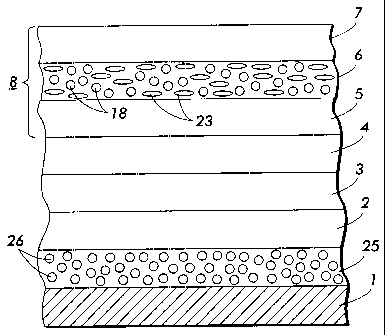
technique. Referring to Figure 2, typically, a flexible or rigid substrate 1
is
provided with an electrically conductive surface or coating 2.
The substrate may be opaque or substantially transparent and may
comprise any suitable material having the required mechanical properties.
Accordingly, the substrate may comprise a layer of an electrically non-
conductive or conductive material such as an inorganic or an organic
composition. As electrically non-conducting materials, there may be employed
various resins known for this purpose including polyesters, polycarbonates,
polyamides, polyurethanes, and the like which are flexible as thin webs. An
electrically conducting substrate may be any metal, for example, aluminum,
-7-
CA 02514508 2007-10-03
nickel, steel, copper, and the like or a polymeric material, as described
above,
filled with an electrically conducting substance, such as carbon, metallic
powder, and the like or an organic electrically conducting material. The
electrically insulating or conductive substrate may be in the form of an
endless
flexible belt, a web, a rigid cylinder, a sheet and the like. The thickness of
the
substrate layer depends on numerous factors, including strength desired and
economical considerations. Thus, for a drum, this layer may be of substantial
thickness of, for example, up to many centimeters or of a minimum thickness
of less than a millimeter. Similarly, a flexible belt may be of substantial
thickness, for example, about 250 micrometers, or of minimum thickness less
than 50 micrometers, provided there are no adverse effects on the final
electrophotographic device.
In embodiments where the substrate layer is not conductive, the
surface thereof may be rendered electrically conductive by an electrically
conductive coating 2. The conductive coating may vary in thickness over
substantially wide ranges depending upon the optical transparency, degree of
flexibility desired, and economic factors. Accordingly, for a flexible
photoresponsive imaging device, the thickness of the conductive coating may
be between about 20 angstroms to about 750 angstroms, or from about 100
angstroms to about 200 angstroms for an optimum combination of electrical
conductivity, flexibility and light transmission. The flexible conductive
coating
may be an electrically conductive metal layer formed, for example, on the
substrate by any suitable coating technique, such as a vacuum depositing
technique or electrodeposition. Typical metals include aluminum, zirconium,
niobium, tantalum, vanadium and hafnium, titanium, nickel, stainless steel,
chromium, tungsten, molybdenum, and the like.
An optional hole blocking layer 3 may be applied to the substrate 1 or
coatings. Any suitable and conventional blocking layer capable of forming an
electronic barrier to holes between the adjacent photoconductive layer 8 (or
electrophotographic imaging layer 8) and the underlying conductive surface 2
of substrate 1 may be used.
An optional adhesive layer 4 may be applied to the hole-blocking layer
3. Any suitable adhesive layer well known in the art may be used. Typical
-8-
CA 02514508 2007-10-03
adhesive layer materials include, for example, polyesters, polyurethanes, and
the like. Satisfactory results may be achieved with adhesive layer thickness
between about 0.05 micrometer (500 angstroms) and about 0.3 micrometer
(3,000 angstroms). Conventional techniques for applying an adhesive layer
coating mixture to the hole blocking layer include spraying, dip coating, roll
coating, wire wound rod coating, gravure coating, Bird applicator coating, and
the like. Drying of the deposited coating may be effected by any suitable
conventional technique such as oven drying, infrared radiation drying, air
drying and the like.
At least one electrophotographic imaging layer 8 is formed on the
adhesive layer 4, blocking layer 3 or substrate 1. The electrophotographic
imaging layer 8 may be a single layer (7 in Figure 2) that performs both
charge-generating and charge transport functions as is well known in the art,
or it may comprise multiple layers such as a charge generator layer 5 and
charge transport layer 6 and overcoat 7.
The charge generating layer 5 can be applied to the electrically
conductive surface, or on other surfaces in between the substrate 1 and
charge generating layer 5. A charge blocking layer or hole-blocking layer 3
may optionally be applied to the electrically conductive surface prior to the
application of a charge generating layer 5. If desired, an adhesive layer 4
may
be used between the charge blocking or hole-blocking layer 3 and the charge
generating layer 5. Usually, the charge generation layer 5 is applied onto the
blocking layer 3 and a charge transport layer 6, is formed on the charge
generation layer 5. This structure may have the charge generation layer 5 on
top of or below the charge transport layer 6.
Charge generator layers may comprise amorphous films of selenium
and alloys of selenium and arsenic, tellurium, germanium and the like,
hydrogenated amorphous silicon and compounds of silicon and germanium,
carbon, oxygen, nitrogen and the like fabricated by vacuum evaporation or
deposition. The charge-generator layers may also comprise inorganic
pigments of crystalline selenium and its alloys; Group II-VI compounds; and
organic pigments such as quinacridones, polycyclic pigments such as
dibromo anthanthrone pigments, perylene and perinone diamines, polynuclear
-9-
CA 02514508 2007-10-03
aromatic quinones, azo pigments including bis-, tris- and tetrakis-azos; and
the like dispersed in a film forming polymeric binder and fabricated by
solvent
coating techniques.
Phthalocyanines have been employed as photogenerating materials for
use in laser printers using infrared exposure systems. Infrared sensitivity is
required for photoreceptors exposed to low-cost semiconductor laser diode
light exposure devices. The absorption spectrum and photosensitivity of the
phthalocyanines depend on the central metal atom of the compound. Many
metal phthalocyanines have been reported and include, oxyvanadium
phthalocyanine, chloroaluminum phthalocyanine, copper phthalocyanine,
oxytitanium phthalocyanine, chlorogallium phthalocyanine, hydroxygallium
phthalocyanine magnesium phthalocyanine and metal-free phthalocyanine.
The phthalocyanines exist in many crystal forms, and have a strong influence
on photogeneration.
Any suitable polymeric film forming binder material may be employed
as the matrix in the charge-generating (photogenerating) binder layer. Typical
polymeric film forming materials include those described, for example, in U.S.
Pat. No. 3,121,006. Thus, typical organic polymeric film forming binders
include thermoplastic and thermosetting resins such as polycarbonates,
polyesters, polyamides, polyurethanes, polystyrenes, polyaryiethers,
polyarylsulfones, polybutadienes, polysulfones, polyethersulfones,
polyethylenes, polypropylenes, polyimides, polymethylpentenes,
polyphenylene sulfides, polyvinyl acetate, polysiloxanes, polyacrylates,
polyvinyl acetals, polyamides, polyimides, amino resins, phenylene oxide
resins, terephthalic acid resins, phenoxy resins, epoxy resins, phenolic
resins,
polystyrene and acrylonitrile copolymers, polyvinylchloride, vinylchloride and
vinyl acetate copolymers, acrylate copolymers, alkyd resins, cellulosic film
formers, poly(amideimide), styrenebutadiene copolymers, vinylidenechloride-
vinylchloride copolymers, vinylacetate-vinylidenechloride copolymers, styrene-
alkyd resins, polyvinylcarbazole, and the like. These polymers may be block,
random or alternating copolymers.
The photogenerating composition or pigment is present in the resinous
binder composition in various amounts. Generally, however, from about 5
-10-
CA 02514508 2007-10-03
percent by volume to about 90 percent by volume of the photogenerating
pigment is dispersed in about 10 percent by volume to about 95 percent by
volume of the resinous binder, or from about 20 percent by volume to about
30 percent by volume of the photogenerating pigment is dispersed in about 70
percent by volume to about 80 percent by volume of the resinous binder
composition. In one embodiment, about 8 percent by volume of the
photogenerating pigment is dispersed in about 92 percent by volume of the
resinous binder composition. The photogenerator layers can also fabricated
by vacuum sublimation in which case there is no binder.
Any suitable and conventional technique may be used to mix and
thereafter apply the photogenerating layer coating mixture. Typical
application
techniques include spraying, dip coating, roll coating, wire wound rod
coating,
vacuum sublimation and the like. For some applications, the generator layer
may be fabricated in a dot or line pattern. Removing of the solvent of a
solvent
coated layer may be effected by any suitable conventional technique such as
oven drying, infrared radiation drying, air drying and the like.
The charge transport layer 6 may comprise a charge transporting small
molecule 23 dissolved or molecularly dispersed in a film forming electrically
inert polymer such as a polycarbonate. The term "dissolved" as employed
herein is defined herein as forming a solution in which the small molecule is
dissolved in the polymer to form a homogeneous phase. The expression
"molecularly dispersed" is used herein is defined as a charge transporting
small molecule dispersed in the polymer, the small molecules being dispersed
in the polymer on a molecular scale. Any suitable charge transporting or
electrically active small molecule may be employed in the charge transport
layer of this invention. The expression charge transporting "small molecule"
is
defined herein as a monomer that allows the free charge photogenerated in
the transport layer to be transported across the transport layer. Typical
charge
transporting small molecules include, for example, pyrazolines such as 1-
phenyl-3-(4'-diethylamino styryl)-5-(4"-diethylamino phenyl)pyrazoline,
diamines such as N,N'-diphenyl-N,N'-bis(3-methylphenyl)-(1,1'-biphenyl)-4,4'-
diamine, hydrazones such as N-phenyl-N-methyl-3-(9-ethyl)carbazyl
hydrazone and 4-diethyl amino benzaldehyde-1,2-diphenyl hydrazone, and
-11-
CA 02514508 2007-10-03
oxadiazoles such as 2,5-bis (4-N,N'-diethylaminophenyl)-1,2,4-oxadiazole,
stilbenes and the like. However, to avoid cycle-up in machines with high
throughput, the charge transport layer should be substantially free (less than
about two percent) of di or triamino-triphenyl methane. As indicated above,
suitable electrically active small molecule charge transporting compounds are
dissolved or molecularly dispersed in electrically inactive polymeric film
forming materials. A small molecule charge transporting compound that
permits injection of holes from the pigment into the charge generating layer
with high efficiency and transports them across the charge transport layer
with
very short transit times is N,N'-diphenyl-N,N'-bis(3-methylphenyl)-(1,1'-
biphenyl)-4,4'-diamine. If desired, the charge transport material in the
charge
transport layer may comprise a polymeric charge transport material or a
combination of a small molecule charge transport material and a polymeric
charge transport material.
Any suitable electrically inactive resin binder insoluble in the alcohol
solvent used to apply the overcoat layer 7 may be employed in the charge
transport layer of this invention. Typical inactive resin binders include
polycarbonate resin, polyester, polyarylate, polyacrylate, polyether,
polysulfone, and the like. Molecular weights can vary, for example, from about
20,000 to about 150,000. Examples of binders include polycarbonates such
as poly(4,4'-isopropylidene-diphenylene)carbonate (also referred to as
bisphenol-A-polycarbonate, poly(4,4'-cyclohexylidinediphenylene) carbonate
(referred to as bisphenol-Z polycarbonate), poly(4,4'-isopropylidene-3,3'-
dimethyl-diphenyl)carbonate (also referred to as bisphenol-C-polycarbonate)
and the like. Any suitable charge transporting polymer may also be used in
the charge transporting layer. The charge transporting polymer should be
insoluble in the alcohol solvent employed to apply the overcoat layer. These
electrically active charge transporting polymeric materials should be capable
of supporting the injection of photogenerated holes from the charge
generation material and be capable of allowing the transport of these holes
there-through.
Any suitable and conventional technique may be used to mix and
thereafter apply the charge transport layer coating mixture to the charge
-12-
CA 02514508 2007-10-03
generating layer. Typical application techniques include spraying, dip
coating,
roll coating, wire wound rod coating, and the like. Drying of the deposited
coating may be effected by any suitable conventional technique such as oven
drying, infrared radiation drying, air drying and the like.
Generally, the thickness of the charge transport layer is between about
and about 50 micrometers, but thicknesses outside this range can also be
used. The hole transport layer should be an insulator to the extent that the
electrostatic charge placed on the hole transport layer is not conducted in
the
absence of illumination at a rate sufficient to prevent formation and
retention
10 of an electrostatic latent image thereon. In general, the ratio of the
thickness
of the hole transport layer to the charge generator layers can be maintained
from about 2:1 to 200:1 and in some instances as great as 400:1. The charge
transport layer, is substantially non-absorbing to visible light or radiation
in the
region of intended use but is electrically "active" in that it allows the
injection
of photogenerated holes from the photoconductive layer, i.e., charge
generation layer, and allows these holes to be transported through itself to
selectively discharge a surface charge on the surface of the active layer.
The thickness of the continuous overcoat layer selected depends upon
the abrasiveness of the charging (e.g., bias charging roll), cleaning (e.g.,
blade or web), development (e.g., brush), transfer (e.g., bias transfer roll),
etc., in the system employed and can range up to about 10 micrometers. In
embodiments, the thickness is from about 1 micrometer and about 5
micrometers. Any suitable and conventional technique may be used to mix
and thereafter apply the overcoat layer coating mixture to the charge-
generating layer. Typical application techniques include spraying, dip
coating,
roll coating, wire wound rod coating, and the like. Drying of the deposited
coating may be effected by any suitable conventional technique such as oven
drying, infrared radiation drying, air drying, and the like. The dried
overcoating
of this invention should transport holes during imaging and should not have
too high a free carrier concentration. Free carrier concentration in the
overcoat increases the dark decay. In embodiments, the dark decay of the
overcoated layer should be about the same as that of the unovercoated
device.
-13-
CA 02514508 2007-10-03
An anti-curl backing layer may be present on the substrate, on the side
opposite the charge transport layer. This layer is positioned on the substrate
to prevent curling of the substrate.
An inorganic material surface grafted or surface anchored with a
charge transport moiety can be added to at least one layer in the
photoreceptor. Such layers include the blocking layer 3 of Figure 2, the
charge transporting layer 6 of Figure 2, the overcoat layer 7 of Figure 2, and
other layers. In embodiments, the surface grafted inorganic material can be
added to the charge transport layer 6 as filler 18, or the blocking/undercoat
layer 3 as filler 26.
An inorganic filler is surface grafted with a charge transport moiety or
component. Herein, "charge transport moiety" or "charge transport
component" refers to part of a hole-transport molecule or part of an electron
transport molecule. A charge transport molecule is an electron transport
molecule or a hole-transporting molecule. A hole-transport molecule functions
to conduct holes, and an electron transport molecule functions to conduct
electrons.
In embodiments, the inorganic material is relatively simple to disperse,
has relatively high surface area to unit volume ratio, has a larger
interaction
zone with dispersing medium, is non-porous, and/or chemically pure. Further,
in embodiments, the inorganic material is highly crystalline, spherical,
and/or
has a high surface area.
Examples of inorganic materials include silica, metals, metal alloys,
and metal oxide fillers such as metal oxides of scandium, titanium, vanadium,
chromium, manganese, iron, cobalt, nickel, copper, zinc, yttrium, zirconium,
niobium, molybdenum, technetium, ruthenium, rhodium, palladium, silver,
cadmium, hafnium, tantalum, tungsten, rhenium, osmium, iridium, platinum,
gold, mercury, unnilquadium, unnilpentium, and unnilhexium (unh inner
transition elements of lanthanides of lanthanum, cerium, praseodymium,
neodymium, promethium, samarium, europium, gadolinium, terbium,
dysprosium, holmium, erbium, thulium, ytterbium, and lutetium; actinides of
actinium, thorium, protactinium, uranium, neptunium, plutonium, americium,
-14-
CA 02514508 2007-10-03
curium, berkelium, californium, einsteinium, fermium, mendelevium, nobelium,
and lawrencium; perovskites of SrTiO3, CaTiOc; oxides of metals of the
second main group of beryllium, magnesium, calcium, strontium, barium,
radium; oxides of metals of the third main group of boron, aluminum, gallium,
indium, and thallium; oxides of metals of a fourth main group of silicon,
germanium, tin and lead; a member wherein the oxide is titanium dioxide; a
member wherein the oxide is anatase titanium dioxide, and the like.
Specific examples include metal oxides such as titanium dioxide,
silicon oxide, aluminum oxide, chromium oxide, zirconium oxide, zinc oxide,
tin oxide, iron oxide, magnesium oxide, manganese oxide, nickel oxide,
copper oxide, conductive antimony pentoxide, and indium tin oxide, and the
like, and mixtures thereof.
The inorganic material can be prepared via plasma synthesis or vapor
phase synthesis, in embodiments. This synthesis distinguishes these
particulate fillers from those prepared by other methods (particularly
hydrolytic
methods), in that the fillers prepared by vapor phase synthesis are non-
porous as evidenced by their relatively low BET values. An example of an
advantage of such prepared fillers is that the crystalline-shaped inorganic
materials are less likely to absorb and trap gaseous corona effluents.
In embodiments, the grafted inorganic material is added to the layer or
layers of the photosensitive member in an amount of from about 0.1 to about
80 percent, from about 3 to about 60 percent, or from about 5 to about 40
percent by weight of total solids. Amount by weight of total solids refers to
the total solids amount in the layer, including amounts of resins, polymers,
fillers, and the like solid materials.
In embodiments, the inorganic material can be small, such as, for example, a
nano-size inorganic material.
Examples of nano-size fillers include fillers having an average particle
size of from about 1 to about 250 nanometers, or from about 1 to about 199
nanometers, or from about 1 to about 195 nanometers, or from about 1 to
about 175 nanometers, or from about 1 to about 150 nanometers, or from
about 1 to about 100 nanometers, or from about 1 to about 50 nanometers.
-15-
CA 02514508 2007-10-03
In embodiments, the inorganic material filler has a BET/surface area of from
about 10 to about 200, or from about 20 to about 100, or from about 20 to
about 50, or about 42 m2/g.
In embodiments, the inorganic material filler is grafted or anchored with
a charge transport moiety. The charge transport moiety comprises an
anchoring group, which facilitates anchoring or grafting of the charge
transport
moiety to the inorganic material. Suitable anchoring groups include those
selected from the group consisting of silanes, silicates, silanol,
phosphonate,
carboxylate, enediolate, carboxylic acids, hydroxyl group, phosphonic acids,
and ene-diols.
The charge transport moiety further comprises a linkage attaching the
charge transport moiety to the anchoring group. The linkage and charge
transport moiety are then grafted onto the inorganic material. The anchoring
group facilitates anchoring of the charge transport moiety (with linking
group)
to the inorganic material.
Generally, the process for surface grafting the charge transport moiety
or component onto the inorganic material includes the scheme as show in
Figure 3. In Figure 3, F represents the charge transport moiety or component
on the charge transport molecule; L represents a divalent linkage, such as,
for
example, alkylene, arylene, and others; and X represents an anchoring or
grafting group, such as a silane, silicate, silanol, carboxylate, a carboxylic
acid, a hydroxyl group, a phosphonic acid, phosphonate, endiolate, or an ene-
diol group.
In embodiments, the surface grafted inorganic material is prepared by
reacting the anchoring or grafting group with the reactive surface of the
inorganic material, such as a metal oxide. This forms a charge-transporting
shell on the core of the inorganic material. The surface treatment can be
carried out by mixing the inorganic material with the molecule containing
charge transport component or moiety and anchoring or grafting group in an
organic solvent to form a dispersion of the inorganic particle with the charge
transport moieties or molecules containing the anchoring groups. The mixing
can be carried out at a temperature ranging from about 25 C to about 250 C,
-16-
CA 02514508 2007-10-03
or from about 25 C to about 200 C for a time, such as for several hours. After
the surface treatment, the excess surface treating agents can be removed by
washing with an organic solvent. The attachment of the organic charge
transport molecules to the inorganic material can be confirmed by FTIR and
TGA analysis.
Examples of linkages include linkages comprising from about 1 to
about 15 carbons, or from about 1 to about 9 carbons, such as methylene,
dimethylene, trimethylene, tetrmethylene and the like, and alkylenes
containing a component selected from the group consisting of esters, ethers,
thio-ethers, amides, ketones, and urethanes.
Charge transport moiety is defined as a moiety or component having a
function of transporting holes or electrons. The charge transport moiety may
be a hole transport moiety or an electron transport moiety.
In embodiments, the charge transport moiety is selected from hole
transporting moieties or components such as triarylamines, pyrazolines such
as 1-phenyl-3-(4'-diethylamino styryl)-5-(4"-diethylamino phenyl)pyrazoline,
hydrazones such as N-phenyl-N-methyl-3-(9-ethyl)carbazyl hydrazone and 4-
diethyl amino benzaidehyde-1,2-diphenyl hydrazone, and phthalocyanines,
metal phthalocyanines, oxadiazoles such as 2,5-bis (4-N,N'-
diethylaminophenyl)-1,2,4-oxadiazole, stilbenes and the like. Other
examples include amines such as aromatic amines, di-, tri- and tertiary
amines, and other amines, specific examples of which include N,N-diphenyl-
(1,1'-biphenyl)-4-amine, N,N-diphenyl-(alkylphenyl)-amine, N,N'-diphenyl-
N,N'-bis(3-methylphenyl)-(1,1'-biphenyl)-4,4'-diamine, N,N'-diphenyl-N,N'-
bis(alkylphenyl)-1,1-biphenyl-4,4'-diamine wherein alkyl is selected from the
group consisting of methyl, ethyl, propyl, butyl, hexyl, and the like; and
N,N'-
diphenyl-N,N'-bis(halophenyl)-1,1'-biphenyl-4,4'- diamine wherein the halo
substituent is preferably a chloro substituent, triarylamines, and the like.
More specifically, the hole transport moiety or component is selected
from the group consisting of
-17-
CA 02514508 2007-10-03
R4 Ra R4 R3
Ri RZ \ / _\ R, Rz \ /
N \ / /-\ N N \ / / \ N
R5 R6 R5 R6
R11 Ris R15
Ri3 R14 R14 R13 R16 R16
O-N O-N
R12 R\ /12 RP R17
RZO Ria Riv R Ria R~9
R21 20 R21
N ~ N ~
6R22 I~
RZ3 R~ Rz2
R7
R8 R7
R$
N / \ \
N
- \ /
Ry
R9
RIo
RIo
wherein R, to R23 are independently selected from a hydrogen atom, an alkyl
with from about 1 to about 10 carbon atoms, a cyclic alkyl with from about 1
to
about 10, an alkoxyl group with from about 1 to about 5 carbon atoms, and
halogen atoms.
The hole transport moiety or component having an anchoring group is
further selected from a group consisting of
-18-
CA 02514508 2007-10-03
R27
n
R27n - Li Si-(OR26)3-n
R24 _ \ I N I/ L S~-(OR213-n
&aN b R25 R27n
24 / \ "R27
R \ I N I/ L-Si\(OR26)3-n
R27 n N
O_L-Si"
(OR26)3 n
L, (OR213-n
Si- R27
OH OH
R24 / ~ ~\ L /\ OH PL--~ OH
\ N / - -
~ -
R25 b
wherein R24 and R25 are independently selected from a hydrogen atom, an
alkyl with from about 1 to about 10 carbon atoms, a cyclic alkyl with from
about 1 to about 10 carbon atoms, an alkoxyl group with from about I to
about 5 carbon atoms, and halogen atoms; R26 and R27 are independently
selected from an alkyl with from about 1 to about 10 carbon atoms, and an
aryl with from about 6 to about 30 carbon atoms; n is a number of 0, 1, or 2;
L
is a divalent group of an alkylene or a substituted alkylene with from about 1
to about 10 carbon atoms, or an arylene or substituted arylene with from
about 6 to about 30 carbon atoms, wherein said divalent group further
contains oxygen, nitrogen, and sulfur atoms.
Other examples of charge transporting moieties include electron
transporting moieties or components such as aromatic imides such as
naphthalimides and diimides such as naphthalenetetracarboxylic diimide,
peryienetetracarboxylic diimide, and the like, and more specifically N-
pentyl,N'-propylcarboxyl-1,4,5,8-naphthalenetetracarboxylic diimide, N-(1-
-19-
CA 02514508 2007-10-03
methyl)hexyl,N =propylcarboxyl-1,7,8,13-perylenetetracarboxylic diimide, and
the like; fluorenylidene malonitriles such as carboxyfluorenylidene
malononitrile (CFM); quinones such as anthraquinones, carboxybenzyl
naphthaquinone, and the like.
More specifically, the electron transport component with an anchoring
group is selected from the group consisting of
O O O O
R28-N N-L'-COOH R29- N - N-L'-COOH
O O O O
O - O O O
26
Rzg N \ / N-L=S~R26n R29 N - N-L'-S"RR27(3n_~)
L R27(3.n)
O \ / O O \ / - O
0 0 OH
O
O OH
R29 N - / N-L' / \ OH
R N N-L' /-\ OH O \ / -\ O
O O
R26 OH
COOH '
c:IIL_Sj27
\ \ I ~ -
CN CN CN CN CN CN
O OH
OH O I\
/ I I \ OVCOOH R2e
L'- S-27
R (3"")
O
wherein R26 and R27 are independently selected from an alkyl with from about
1 to about 10 carbon atoms, and an aryl with from about 6 to about 30 carbon
atoms; R28 and R29 are independently selected from an alkyl with from about 1
to about 10 carbon atoms, and an aryl with from about 6 to about 30 carbon
atoms; n is a number of 0, 1, or 2; L' is a divalent group of an alkylene or a
substituted alkylene with from about 1 to about 10 carbon atoms, or an
aryiene or substituted aryiene with from about 6 to about 30 carbon atoms,
-20-
CA 02514508 2007-10-03
wherein said divalent group further contains oxygen, nitrogen, and/or sulfur
atoms.
In embodiments, the grafted inorganic material can be prepared by sol-
gel process. The sol-gel process comprises, for example, the preparation of
the sol, gelation of the sol, and removal of the solvent. The preparation of a
metal oxide sol is disclosed in, for example, B. O'Regan, J. Moser, M.
Anderson and M. Gratzel, J. Phys. Chem., vol. 94, pp. 8720-8726 (1990), C.
J. Barbe, F. Arendse, P. Comte, M. Jirousek, F. Lenzmann, V. Shklover and
M. Gratzel, J. Am. Ceram. Soc., vol. 80(12), pp. 3157-3171 (1997), Sol-Gel
Science, eds. C. J. Brinker and G. W. Scherer (Academic Press Inc., Toronto,
1990), 21-95, U.S. Pat. No. 5,350,644, M. Graetzel, M. K. Nazeeruddin and B.
O'Regan, Sep. 27, 1994, P. Arnal, R. J. P. Corriu, D. Leclercq, P. H. Mutin
and A. Vioux, Chem. Mater., vol. 9, pp. 694-698 (1997). Chemical additives
can be reacted with a precursor metal oxide to modify the hydrolysis-
condensation reactions during sol preparation and which precursors have
been disclosed in J. Livage, Mat. Res. Soc. Symp. Proc., vol. 73, pp. 717-724
(1990). Sol refers for example, to a colloidal suspension, solid particles, in
a
liquid, reference P. J. Flory, Faraday Disc., Chem. Society, 57, pages 7-18
for
example, 1974, and gel refers, for example, to a continuous solid skeleton
enclosing a continuous liquid phase, both phases being of colloidal
dimensions, or sizes. A gel can be formed also by covalent bonds or by chain
entanglement.
A sol can be considered a colloidal suspension of solid particles in a
liquid, and wherein the gel comprises continuous solid and fluid phases of
colloidal dimensions, with a colloid being comprised of a suspension where
the dispersed phase is approximately 1 to 1,000 nanometers in diameter, from
about 1 to about 250 nanometers, from about 1 to about 199 nanometers,
from about 1 to about 195 nanometers, from about 1 to about 175
nanometers, from about 1 to about 150 nanometers, from about 1 to about
100 nanometers, or from about 1 to about 50 nanometers.
As the gel is dried and solvent removed, a film is obtained. The sol-gel
process has been described in Sol-Gel Sciences, eds. C. J. Brinker and G. W.
Scherer (Academic Press Inc., Toronto, 1990).
-21-
CA 02514508 2007-10-03
A first step in the preparation of the sol-gel blocking layer is to prepare
the sol and graft the charge transporting moiety onto the sol. The inorganic
material, such as a metal oxide such as, for example, alumina, titania, zinc
oxide, or the like, and an organic solvent, can be mixed along with the charge
transporting moiety. Heating and stirring for up to several hours, such as
from
about 1 to about 20, or from about 3 to about 10 hours, may follow to effect
mixing. After the surface treatment, the excess surface treatment agents can
be removed by washing with an organic solvent.
The following Examples further define and describe embodiments of
the present invention. Unless otherwise indicated, all parts and percentages
are by weight.
EXAMPLES
Example 1
Preparation of Aluminum Oxide Nano-particles Anchored with
Triarylamine Hole Transport Molecule Containing Silane Anchoring Group
The following formula is a silane anchoring group that can be used. It
is referred to herein as "Compound I."
OR
CH2CHZCOOCH2CHZCHZSi- OR
- Me
N
OR
CHZCHZCOOCHZCHZCHzSi- OR
M.
Aluminum oxide nano-particles having an average particle size of about 39
nanometers (10g) and Compound I(0.1 grams) were sonicated in dodecane
(100 grams) for 20 minutes. This was followed by heating and stirring the
dispersion for 12 hours. After the surface treatment, the excess surface
treatment agents were removed by washing with an organic solvent. The
isolated particles were dried at 120 C for about 12 hours. The attachment of
the organic charge transport molecules was confirmed by FTIR and TGA
analysis.
-22-
CA 02514508 2007-10-03
Example 2
Preparation and Testing of Photoreceptor having Aluminum Oxide
Nano-particles Anchored with Hole Transport Molecule Containing Silane
Anchoring Groups Dispersed in Charge Transport Layer
On a 75 micron thick titanized MYLAR substrate was coated by draw
bar technique, a barrier layer formed from hydrolyzed gamma
aminopropyltriethoxysilane having a thickness of 0.005 micron. The barrier
layer coating composition was prepared by mixing
3-aminopropyltriethoxysilane with ethanol in a 1:50 volume ratio. The coating
was allowed to dry for 5 minutes at room temperature, followed by curing for
10 minutes at 110 C in a forced air oven. On top of the blocking layer was
coated a 0.05 micron thick adhesive layer prepared from a solution of 2
weight percent of a DuPont 49K (49,000) polyester in dichloromethane. A 0.2
micron photogenerating layer was then coated on top of the adhesive layer
with a wire wound rod from a dispersion of hydroxy gallium phthalocyanine
Type V (22 parts) and a vinyl chloride/vinyl acetate copolymer, VMCH (Mn =
27,000, about 86 weight percent of vinyl chloride, about 13 weight percent of
vinyl acetate and about 1 weight percent of maleic acid) available from Dow
Chemical (18 parts), in 960 parts of n-butylacetate, followed by drying at
100 C for 10 minutes. Subsequently, a 24 m thick charge transport layer
(CTL) was coated on top of the photogenerating layer by a draw bar from a
dispersion of the surface grafted alumina particles of Example 1 (9 parts),
N,N'-diphenyl-N,N-bis(3-methylphenyl)-1,1'-biphenyl-4,4'-diamine (67.8 parts),
1.7 parts of 2,6-Di-tert-butyl-4methylphenol (BHT) from Aldrich and a
polycarbonate, PCZ-400 [poly(4,4'-dihydroxy-diphenyl-1-1-cyclohexane), M,=
40,000] available from Mitsubishi Gas Chemical Company, Ltd. (102 parts) in
a mixture of 410 parts of tetrahydrofuran (THF) and 410 parts of
monochlorobenzene. The CTL was dried at 115 C for 60 minutes.
The above dispersion with solid components of surface treated alumina
particles of Example I was prepared by pre-dispersed alumina in a sonicator
bath (Branson Ultrasonic Corporation Model 2510R-MTH) with
monochlorobenzene and then added to the rest charge transport liquid to form
-23-
CA 02514508 2007-10-03
a stable dispersion and roll milled for an extended period of time of 6 to 36
hours before coating. The electrical and wear properties of the above
resulting photoconductive member were measured in accordance with the
procedure described in Example IV. The results are shown in Table 1 below.
TABLE 1
Device Vddp E1/2 Dark Decay Vr Wear
(-V) (Ergs/cm)2 (V@ 500 ms) (V)
(nm/k cycles)
Control Device 811 1.36 22 4.0 41.5
Without A1203
Device with A1203 811 1.31 20 1.6 15.2
Example 3
Preparation of Titanium Oxide Nanoparticles Surface Grafted with CFM
Titanium oxide nano-particles having an average particle size of about
70 nanometer (40 g) and CFM (0.4 g), were sonicated in tetrahydrofuran (400
g). This was followed by heating and stirring the dispersion at about 55-C for
12 hours. After the surface treatment, the excess surface treatment agents
were removed by washing with an organic solvent. The isolated particles were
dried at about 100 C for 12 hours. The attachment of the organic charge
transport molecules was confirmed by FTIR and TGA analysis. The following
is the structure of CFM:
COOH
CN CN
Example 4
Preparation of Titanium Oxide Nanoparticles Surface Grafted with N-
pentyl,N=propylcarboxyl-1,4,5,8-naphthalenetetracarboxylic Diimide
-24-
CA 02514508 2007-10-03
Titanium oxide nano-particles having an average particle size of about
70 nanometer (40 g) and N-pentyl,N' propylcarboxyl-1,4,5,8-
naphthalenetetracarboxylic diimide (0.4 g) were sonicated in tetrahydrofuran
(400 g). This was followed by heating and stirring the dispersion at about
55 C for 12 hours. After the surface treatment, the excess surface treatment
agents were removed by washing with an organic solvent. The isolated
particles were dried at about 100 C for 12 hours. The attachment of the
organic charge transport molecules was confirmed by FTIR and TGA
analysis.
Example 5
Preparation of Titanium Oxide Nanoparticles Surface Grafted with IV
(1-methyl)hexyi,N=propylcarboxyl-1,7,8,13-perylenetetracarboxylic Diimide
Titanium oxide nano-particles having an average particle size of about
70 nanometer (40 g) and N-(1-methyl)hexyl,N=propylcarboxyl-1,7,8,13-
perylenetetracarboxylic diimide (0.4 g) were sonicated in chlorobenzene (400
g). This was followed by heating and stirring the dispersion at about 130 C
for
12 hours. After the surface treatment, the excess surface treatment agents
were removed by washing with THF. The isolated particles were dried at
about 100 C for 12 hours. The attachment of the organic charge transport
molecules was confirmed by FTIR and TGA analysis.
Example 6
Preparation of Titanium Oxide Nanoparticles Surface Grafted with
Alizarin
Titanium oxide nano-particles having an average particle size of about
70 nanometer (40 g) and alizarin (0.4 g), were sonicated in tetrahydrofuran
(400 g). This was followed by heating and stirring the dispersion at about
55 C for 12 hours. After the surface treatment, the excess surface treatment
agents were removed by washing with an organic solvent. The isolated
particles were dried at about 100 C for 12 hours. The attachment of the
-25-
CA 02514508 2007-10-03
organic charge transport molecules was confirmed by FTIR and TGA
analysis.
Example 7
Preparation and Testing Photoreceptor having Surface Grafted
Titanium Oxide Filler Dispersed in Undercoat Layer
The dispersion of the undercoat (hole blocking) was prepared by
mixing T;02 particles (30 grams), Varcum 29159 (40 grams, 50% solid in
butanol/xylene=50/50, OxyChem), and 30 grams of 50/50 butanol/xylene. An
amount of 300 grams of cleaned Zr02 beads (0.4-0.6mm) were added and the
dispersion was roll milled for 7 days at 55 rpm. The particle size of the
dispersion was determined by a Horiba particle analyzer. The results were
0.07 0.06pm, and a surface area of 24.9m2/g for alizarin-grafted
TiO2Narcum dispersion.
A 30-millimeter aluminum drum substrate was coated using known
Tsukiage coating technique with a hole blocking layer from the above
dispersions. After drying at 145 C for 45 minutes, blocking layers or
undercoat
layers (UCL) with varying thickness were obtained by controlling pull rates.
The thickness varied as 3.9, 6, and 9.6 microns. A 0.2 micron
photogenerating layer was subsequently coated on top of the hole blocking
layer from a dispersion of chlorogallium phthalocyanine (0.60 gram) and a
binder of polyvinyl chloride-vinyl acetate-maleic acid terpolymer (0.40 gram)
in
20 grams of a 1:2 mixture of n-butyl acetate/xylene solvent. Subsequently, a
22-micron charge transport layer (CTL) was coated on top of the
photogenerating layer from a solution of N,N'-diphenyl-N,N-bis(3-methyl
phenyl)-1,1'-biphenyl-4,4'-diamine (8.8 grams) and a polycarbonate, PCZ-400
[poly(4,4'-dihydroxy-diphenyl-l-1-cyclohexane, Mw=40000)] available from
Mitsubishi Gas Chemical Co., Ltd. (13.2 grams) in a mixture of 55 grams of
tetrahydrofuran (THF), and 23.5 grams of toluene. The CTL was dried at
120 C for 45 minutes.
The control devices with untreated Ti02 UCL were prepared by the
same method except that the dispersion used untreated Ti02 as the filler.
-26-
CA 02514508 2007-10-03
The xerographic electrical properties of the imaging members can be
determined by known means, including as indicated herein electrostatically
charging the surfaces thereof with a corona discharge source until the surface
potentials, as measured by a capacitively coupled probe attached to an
electrometer, attained an initial value Vo of about -500 volts. Each member
was exposed to light from a 670 nanometer laser with >100 ergs/cm2
exposure energy, thereby inducing a photodischarge which resulted in a
reduction of surface potential to a Vr value, residual potential. The
following
Table 2 summarizes the electrical performance of these devices, and
illustrates the electron transport enhancement of the illustrative
photoconductive members. The enhancement in electron mobility with
Alizarin- grafted Ti02 UCL was demonstrated by the decrease in Vr with the
same UCL thickness. These parameters indicate that a greater amount of
charge was moved out of the photoreceptor, resulting in a lower residual
potential. The results are shown in Table 2 below.
TABLE 2
UCL thickness Vr (V)
3.9 microns 33
alizarin-Ti02/Varcum UCL 6.0 microns 57
9.6 microns 118
3.9 microns 42
Ti02/Varcum UCL 6.1 microns 79
9.4 microns 174
Examples 8-10
Preparation of Zinc Oxide Nanoparticles Surface Grafted with
Electron Transport Moieties
The zinc oxide nanoparticies surface grafted with electron transport
components were prepared by the same method as for Examples 3-5, except
zinc oxide nanoparticles having an average particle size of about 70
nanometer were used in Example 8-10.
-27-
CA 02514508 2007-10-03
, While the invention has been described in detail with reference to
specific embodiments, it will be appreciated that various modifications and
variations will be apparent to the artisan. All such modifications and
embodiments as may readily occur to one skilled in the art are intended to be
within the scope of the appended claims.
-28-