Note: Descriptions are shown in the official language in which they were submitted.
CA 02515111 2005-08-02
WO 2004/071703 PCT/EP2004/001102
1
GENERATOR FOR ARC WELDER WITH HIGH POWER FACTOR
Technical Field
The present invention relates to a generator to be used in an electric
arc welder; more particularly, the present invention relates to a generator
that converts an alternating single- or three-phase mains current into a
direct
current that is controlled and adapted for the welding arc.
Background Art
The problems that arise in generators for arc welders are linked
mainly to the low power factor of the current absorbed from the power
supply mains.
Additionally, another factor that has a negative effect on the
efficiency of an arc welder provided according to known layouts and
methods is the unpredictable variation of the power supply voltage.
With reference to the background art by way of example, the classic
widely used layout of an electronic welder is shown in Figure 1.
The layout comprises, on the mains side, a first rectifier stage 1
constituted only by diodes, followed by a bank of leveling capacitors 2.
The current thus rectified and leveled supplies an inverter block 3
provided by means of high-frequency electronic switches, which supplies
the primary winding of a transformer 4.
The secondary winding of the transformer 4 is followed by a second
rectifier stage 5.
The current in output from the second rectifier stage 5 is leveled by an
inductor 6 and supplies a welding arc 7.
A generator of this kind, during operation, absorbs from the mains a
current that has a behavior of the type shown in Figure 2.
It is immediately evident that a waveform of this type has a high
harmonic content, and this entails a low power factor.
In this situation, in order to have a high useful power level in the arc
it is necessary to absorb a high RMS value from the mains.
CA 02515111 2011-02-24
2
This entails a considerable negative impact on the power supply network,
since the high harmonic content and the high RMS value of the absorbed current
cause an increase in the heating of the power supply conductors and a
considerable
distortion of the waveform of the voltage of the power supply line, which in
turn
causes an increase in losses in the ferromagnetic cores of the transformers
connected
thereto.
Additionally, the distortion of the waveform introduces considerable noise on
the line.
Further, when the welding generators are of limited power, as occurs for
io those intended to be supplied by domestic utility systems, the high
intensity of the
absorbed RMS current causes the intervention of the thermal protection of the
utility system even though the power delivered on the welding arc is lower
than that
of an equivalent resistive load.
Moreover, as already mentioned, a generator with a layout of the type shown
in Figure 1 inevitably is affected by the variations in the input supply
voltage, and
this reduces considerably the performance of said generator.
In view of these problems, welding generators have been devised that have
additional stages that allow a mains current absorption that is as sinusoidal
as
possible, i.e., render the generator equivalent to a resistive load so as to
be able to
use all the active power available to the user.
Additional stages have also been adopted which have the task of automatically
adapting the generator to the mains voltage variations, ensuring good and
stable
performance of the generator.
Generators with layouts of this type can be of the type shown schematically in
Figure 3.
This layout clearly shows that with respect to the diagram of Figure 1 there
is
the addition of a stage 8 that is interposed between the rectifier block 1 and
the
leveling block 2.
Figure 4 illustrates a typical current profile (Tin) for the generator of
Figure 3.
This stage, termed PFC, can be provided in various kinds.
CA 02515111 2011-02-24
3
Generators of this type are in any case expensive and complicated and
sometimes critical in the choice of the components that need to withstand high
voltages.
Summary of the Invention
It is therefore desirable to provide an arc welding generator that absorbs
from
the mains a current with a high power factor.
It is also desirable to provide an arc welding generator that is not sensitive
to
variations of the power supply voltage drawn from the mains.
It is further desirable to provide a set of circuits in which it is possible
to use
1o components that have a low cost and high efficiency.
Accordingly, in an aspect of the present invention, there is provided a
generator for arc welder of the type composed of a rectifier stage supplied by
the
mains, followed by a PFC stage and by an inverter stage, both of the high-
frequency
type, the latter supplying an output stage for supplying power to a welding
arc.
The PFC stage is composed of: two inductors, which are mutually
magnetically coupled and are arranged in series at the output of the rectifier
stage;
two first high-frequency controlled switches, which are connected between a
common node and two nodes respectively at the outputs of the two inductors;
two
diodes with opposite conduction directions, which are respectively connected
to the
nodes between the switches and mutual inductors; two leveling capacitors,
which are
connected to the output nodes of said diodes and the common of said first
switches;
means being further provided for controlling the succession of the on and off
switchings of said two first switches, so as to shape the current absorbed by
the
rectifier stage, correlating it to the waveform of the line voltage.
The inverter stage, supplied between the common of said first high-frequency
switches and the common node between said capacitors, comprises four triads,
each
composed of a second controlled switch, a diode and a capacitor, connected so
as to
form five nodes, respectively a central node, two intermediate nodes and two
external nodes, said external nodes being connected to the nodes between said
first
switches and the respective diodes, said intermediate nodes being connected to
the
CA 02515111 2011-02-24
4
common of said two first electronic switches with the interposition of a diode
respectively, a capacitor being connected between said intermediate nodes, a
control
device being further provided for the four second switches, the current for
the
output stage that supplies the welding arc being drawn between the common of
the
two first switches and the central node of said four triads of second
controlled
switches, diodes and capacitors.
Brief Description of the Drawings
Further characteristics and advantages of the invention will become better
apparent from the following detailed description of a preferred embodiment
thereof,
to illustrated by way of non-limiting example in the accompanying drawings,
wherein:
Figures 1, 2, 3 and 4 are views of known devices and of operating diagrams
thereof;
Figure 5 is a schematic view of the four stage generator of the present
invention, illustrating in particular its connections;
Figure 6 is a detailed view of the PFC stage shown in Figure 5; and
Figure 7 is a detailed view of the inverter stage shown in Figure 5.
Detailed Description of Exemplary Embodiments
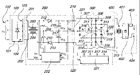
With reference to the Figures 5, 6, and 7, a generator exemplary of an
embodiment of the invention can be ideally divided into four stages, which are
respectively designated by the reference numeral 100 for the mains power
supply
stage, by the reference numeral 200 for the PFC stage, by the reference
numeral 300
for the inverter stage, and by the reference numeral 400 for the output and
arc
supply stage.
As illustrated in Figure 5, the mains power supply stage 100 is composed of a
conventional rectifier block with diodes 101 that is supplied by a mains 102
and can
be single-phase or three-phase.
Two output conductors, designated respectively by the reference numerals
103 and 104, lead out from the stage 101 and continue in the PFC stage 200 in
two
input conductors 201 and 202.
CA 02515111 2011-02-24
As shown in Figures 5 and 6, two inductors 203 and 204 are respectively
connected to the inputs 201 and 202 and are mutually magnetically coupled.
The outputs of the two inductors 203 and 204, designated by the reference
numerals 205 and 206, are connected respectively to a first node 207 and to a
second
5 node 208.
The first terminal of a first controlled switch 209 is connected to the node
207, and the first terminal of a second controlled switch 210 is connected to
the
node 208.
The second terminal of the first controlled switch 209 and the second
terminal of the second controlled switch 210 are connected to a common node
211.
The first terminal of a first diode 212 is connected to the node 207, and the
first terminal of a second diode 213 is connected to the node 208; the two
diodes
have opposite conduction directions.
The second terminal of the first diode 212 is connected to a node 214, and
the second terminal of the second diode 213 is connected to a node 215. The
first
terminal of a first leveling capacitor 216 is connected to the node 214, and
the first
terminal of a second leveling capacitor 217 is connected to the node 215.
The two capacitors 216 and 217 are arranged so as to have mutually opposite
polarities, and their second terminals are connected to a node 218 that is
connected
to the node 211.
The PFC stage 200 has three output conductors, respectively a conductor 219
connected to the node 214, a conductor 220 connected to the node 215, and a
conductor 221 connected to the node 218.
As illustrated in Figure 6, the PFC stage 200 has a control device 222 that
controls the on and off switching of the switches 209 and 210, which are of
the
high-frequency controlled type (IGBT or MOSFET).
The device 222 draws a voltage signal Vin from the input 201 by means of the
connection 223, a current signal Tin from the conductor 205 by means of the
connection 224, a voltage signal Vci from the node 214 or from the capacitor
216 by
CA 02515111 2011-02-24
6
means of the connection 225, and a voltage signal Vc2 from the node 215 or
from
the capacitor 217 by means of the connection 226.
In Figure 6, the connections 227 and 228 designate the control of the
switches 209 and 210.
By means of a suitable control of the succession of on and off switchings of
the two switches 209 and 210, the control device 222 controls the current
absorbed
by the rectified power supply stage 100, shaping it so as to follow the
waveform of
the voltage line, obtained from the signal Vin, so as to have a very low
distortion and
therefore a very high power factor.
By closing the switches 209 and 210, the current in the inductors 203 and 204
increases with a slope that is equal to
Vin/(Li+L2+M12)
where M12 is a coefficient that takes into account the coupling of the two
inductors
while the diodes 212 and 213 are off and L1, L2 respectively correspond to
inductors
203 and 204.
By opening the switches 209 and 210, the current circulates in 203, 212, 216,
217, 213 and 204 so as to charge the leveling capacitors 216 and 217 and
decreases
with a slope equal to
- [Vin - (Vci + Vc2)] / (Li + L2 + M12)
By way of the connection between the node 211 and the node 218, or
between the two switches 209 and 210 with the two capacitors 216 and 217 that
have equal capacitances, the voltage applied to each one of the switches is
equal to
Vc/2, which is half the voltage that occurs with configurations of normal
known
PFC stages.
This allows the use of switches that have a lower breakdown voltage and for
reasons linked to the manufacturing technology of electronic switches allows
to
work at higher switching frequencies, consequently allowing to reduce the
values of
the inductors 203 and 204 and to improve control of the current absorbed from
the
mains.
CA 02515111 2011-02-24
7
As it is known, as the breakdown voltage of electronic switches rises the
proper switching times of said switches also increase, and therefore it
becomes
increasingly necessary to lower the switching frequencies in order to limit
the power
dissipated by said switches.
As shown in Figures 5 and 7, the inverter stage 300 has a high switching
frequency and comprises: a first external node 301, which is connected to the
output
conductor 219 of the PFC stage; a second external node 302, which is connected
to
the output conductor 220; a first intermediate node 303, which is connected to
the
output conductor 221 with the interposition of a diode 304; and a second
intermediate node 305, which is connected to the output conductor 221 with the
interposition of a diode 306.
The diodes 304 and 306 are arranged so as to have opposite conduction
directions.
A first triad of components in a parallel configuration, constituted by a
controlled switch 307, a diode 308 and a capacitor 309, is provided between
the first
external node 301 and the first intermediate node 303.
A second triad of components in a parallel configuration, constituted by a
controlled switch 311, a diode 312 and a capacitor 313, is provided between
the first
intermediate node 303 and a central node 310.
Likewise, a triad of components in a parallel configuration, constituted by a
third controlled switch 314, a diode 315 and a capacitor 316, is provided
between the
second external node 302 and the second intermediate node 305.
A triad of components in a parallel configuration, composed of a fourth
controlled switch 317, a diode 318 and a capacitor 319, is provided between
the
second intermediate node 305 and the central node 310.
There is also a capacitor 320 that is connected between the two intermediate
nodes 303 and 305.
The inverter stage 300 further has a control device 321 for switching on and
off the four controlled switches 307, 311, 317 and 314.
CA 02515111 2011-02-24
8
By way of the connection between the node 322, which is common to the
diodes 304 and 306, and the node 218, the maximum voltage affecting each
controlled switch is halved.
This situation allows to use components that have much higher switching
frequencies and speeds than circuits with a known layout, so that it is
possible to
reduce the dimensions of the magnetic components.
In view of the connection between the PFC stage 200 and the inverter stage
300, by means of the conductors 219, 221 and 220, by way of a suitable on and
off
switching control of the switches it is possible to control the balancing of
the
1o voltages on the capacitors 216 and 217 so as to avoid compromising control
of the
welding current.
As shown in Figure 5, the stage 400 is supplied by the node 322 and by the
node 310, with which the primary winding of a transformer 401 is associated,
said
transformer in turn supplying power to a rectifier 402, in which the output
supplies
the welding arc 404 with the interposition of an inductor 403.