Language selection

Search

Patent 2515196 Summary

Third-party information liability

Some of the information on this Web page has been provided by external sources. The Government of Canada is not responsible for the accuracy, reliability or currency of the information supplied by external sources. Users wishing to rely upon this information should consult directly with the source of the information. Content provided by external sources is not subject to official languages, privacy and accessibility requirements.

Claims and Abstract availability

Any discrepancies in the text and image of the Claims and Abstract are due to differing posting times. Text of the Claims and Abstract are posted:

  • At the time the application is open to public inspection;
  • At the time of issue of the patent (grant).
(12) Patent Application: (11) CA 2515196
(54) English Title: FREE-STANDING DIAMOND STRUCTURES AND METHODS
(54) French Title: STRUCTURES DE DIAMANT AUTOPORTANTES ET PROCEDES
Status: Deemed Abandoned and Beyond the Period of Reinstatement - Pending Response to Notice of Disregarded Communication
Bibliographic Data
(51) International Patent Classification (IPC):
  • C30B 29/04 (2006.01)
  • C23C 16/26 (2006.01)
  • C30B 25/00 (2006.01)
  • C30B 33/08 (2006.01)
(72) Inventors :
  • MEARINI, GERALD T. (United States of America)
  • DAYTON, JAMES A., JR. (United States of America)
(73) Owners :
  • GENVAC AEROSPACE CORPORATION
(71) Applicants :
  • GENVAC AEROSPACE CORPORATION (United States of America)
(74) Agent: EDWARD H. OLDHAMOLDHAM, EDWARD H.
(74) Associate agent:
(45) Issued:
(86) PCT Filing Date: 2004-02-06
(87) Open to Public Inspection: 2004-08-26
Availability of licence: N/A
Dedicated to the Public: N/A
(25) Language of filing: English

Patent Cooperation Treaty (PCT): Yes
(86) PCT Filing Number: PCT/US2004/003518
(87) International Publication Number: WO 2004072319
(85) National Entry: 2005-08-04

(30) Application Priority Data:
Application No. Country/Territory Date
60/445,237 (United States of America) 2003-02-06
60/494,089 (United States of America) 2003-08-12
60/494,095 (United States of America) 2003-08-12

Abstracts

English Abstract


The present invention is directed in one aspect to methods of making free-
standing, internally-supported, three-dimensional objects having an outer
surface comprising a plurality of intersecting facets wherein a sub-set of the
intersecting facets have a diamond layer of substantially uniform thickness.
The diamond layer may be formed by chemical vapor deposition (CVD) over the
surface of a substrate that has been fabricated to form a mold defining the
sub-set of intersecting facets. A backing layer may be formed over at least a
portion of the exposed diamond layer to enhance the rigidity of the layer when
the substrate is removed.


French Abstract

L'invention concerne, dans un aspect, des procédés de fabrication d'objets tridimensionnels autoportants, soutenus de l'intérieur, dont une surface extérieure présente une pluralité de facettes sécantes. Un sous-ensemble des facettes sécantes comporte une couche de diamant d'épaisseur sensiblement uniforme. La couche de diamant peut être formée par dépôt chimique en phase vapeur (CVD) sur la surface d'un substrat ayant été fabriqué pour constituer un moule définissant le sous-ensemble de facettes sécantes. Une couche renfort peut être formée sur au moins une partie de la couche de diamant exposée pour accroître la rigidité de la couche lorsque le substrat est éliminé.

Claims

Note: Claims are shown in the official language in which they were submitted.

WHAT IS CLAIMED IS:
1. A method of making a free-standing, internally-supported, three-
dimensional object, the outer surface of the object comprising a plurality of
intersecting
facets, at least a sub-set of said intersecting facets having a diamond layer
of substantially
uniform depth, said method comprising the steps of:
(a) providing a mold having an exposed surface defining the sub-set of
intersecting facets;
(b) growing a diamond layer of substantially uniform depth over the exposed
surface;
(c) depositing a backing layer over at least a portion of the diamond layer;
and
(d) removing the mold to expose the surface of the diamond layer grown
immediately contiguous to the mold.
2. The method of Claim 1 wherein the mold is a silicon substrate fabricated to
define the sub-set of intersecting facets.
3. The method of Claim 2 wherein the mold is removed by chemical etching.
4. The method of Claim 1 further including the step of pretreating the exposed
surface of the mold to enhance the growth of the diamond layer.
5. The method of Claim 4 wherein carbon atoms are deposited on the exposed
surface of the mold to enhance the growth of the diamond layer.
6. The method of Claim 5 wherein the carbon atoms are deposited on the
exposed surface of the mold by exposing the surface to a carbon containing
plasma.
6

7. The method of Claim 1 wherein the sub-set of intersecting facets includes
planar facets.
8. The method of Claim 1 wherein the sub-set of intersecting facets includes
non-planar facets.
9. A method of fabricating a free-standing object comprising a three-
dimensional structure covered by a diamond film having an exposed surface,
said method
comprising the steps of:
growing a diamond film on a preselected exposed surface of a substrate;
providing a backing on at least a portion of the grown diamond film; and
removing the substrate to expose the diamond surface defined by the
preselected
surface of the substrate on which the diamond was grown.
10. The method of Claim 9 wherein the substrate is silicon.
11. The method of Claim 9 including the further step of pretreating the
preselected exposed surface to enhance the growth of diamond thereon.
12. The method of Claim 11 wherein a carbon seed layer is formed on the
preselected exposed surface of the substrate.
13. The method of Claim 9 wherein the preselected surface of the substrate
includes the intersection of two facets.
14. A method of fabricating a free-standing, internally-supported, three-
dimensional object, the outer surface of the object comprising a plurality of
intersecting
facets, at least a sub-set of said intersecting facets having an exposed
diamond surface,
said method comprising the steps of:
7

growing a diamond film on a preselected exposed surface of a substrate;
providing a backing layer covering at least a portion of the grown diamond
film;
and
removing the substrate so that the exposed diamond surface is the surface
grown
immediately contiguous to the substrate.
15. The method of Claim 14 wherein the substrate is silicon.
16. The method of Claim 15 wherein the substrate is removed by chemical
etching.
17. The method of Claim 14 wherein the backing layer covers the entire
diamond film.
18. The method of Claim 14 wherein the backing layer is electrically
conducting.
19. The method of Claim 14 wherein the backing layer is electrically non-
conducting.
20. The method of Claim 19 wherein the backing layer is epoxy.
21. The method of Claim 14 including the further step of forming a carbon seed
layer on the preselected exposed surface of the substrate to facilitate the
growth of the
diamond film thereon.
22. The method of Claim 21 wherein the diamond seed layer is formed by
exposing the preselected exposed surface of the substrate to a carbon
containing activated
gas.
8

23. The method of Claim 22 wherein the diamond seed layer is formed by:
grounding the substrate;
providing ionized carbon atoms; and
exposing the preselected exposed surface of the substrate to the ionized
carbon
atoms.
24. The method of Claim 22 wherein the activated gas is a plasma.
25. The method of Claim 24 wherein the plasma is formed by energizing a
mixture of hydrogen and hydrocarbon gases.
26. The method of Claim 22 wherein the diamond seed layer is formed by
chemical vapor deposition.
27. The method of Claim 14 wherein the diamond is grown by chemical vapor
deposition.
28. The method of Claim 14 wherein the intersecting facets include planar
facets.
29. The method of Claim 14 wherein the intersecting facets include non-planar
facets.
30. The method of Claim 14 wherein the exposed diamond surface forms the
surface of a waveguide.
31. The method of Claim 14 wherein the object is a bi-polar plate for a fuel
cell.
32. A method of making a free-standing, internally-supported, three-
dimensional object, the outer surface of the object comprising a plurality of
intersecting
9

facets, at least a sub-set of said intersecting facets having a diamond layer
of substantially
uniform depth, said method comprising the steps of:
(a) fabricating a silicon substrate to provide a molding surface defining the
sub-set of intersecting facets;
(b) seeding the molding surface of the substrate with carbon;
(c) growing a diamond layer of substantially uniform depth over the molding
surface of the substrate;
(d) forming an internally-supporting backing layer over the diamond layer; and
(e) chemically etching the substrate to expose the surface of the diamond
layer
grown contiguous to the molding surface of the substrate.
33. The method of Claim 32 wherein molding surface is seeded by chemical
vapor deposition.
34. The method of Claim 32 wherein the diamond layer is grown by chemical
vapor deposition.

Description

Note: Descriptions are shown in the official language in which they were submitted.


CA 02515196 2005-08-04
WO 2004/072319 PCT/US2004/003518
FREE-STANDING DIAMOND STRUCTURES AND METHODS
CLAIM OF PRIORITY
[0001] This application claims the benefit of the filing date priority of U.S.
Provisional Application No. 601445,237 :fled February 6, 2003; No. 60/494,089
filed
August 12, 2003; and No. 60/494,095 filed August 12, 1003.
BACKGR~UND ~F THE INVENTI~N
[0002] The present invention relates to free-standing objects having
laboratory
grown diamond surfaces and methods f~r fabricating such objects. fore
parhicularly, the
present invention is directed to such objects and methods wherein the outer
surface of the
object includes a plurality of intersecting facets having a diamond layer.
[0~03] hiamond is one of the host ~;echnologically and scientifically valuable
materials found in nature due to its combination of high resistance to thermal
shocks
e~~treme hardness, excellent infrared transparency, and excellent
semiconductor ,
proper ties.
[~004] Diamond has the highest l~nown isotropic thermal c~r~ductivity and a
relatively low expansion coefficient thus providing it with desirable
resistance to thermal
shock. Because of these pxoperties, diamond has found increasing use as a
thermal
management material in electronic packaging of devices such as high power
laser diodes,
ultichip anodules, and other microelectronic devices.
[0005] Diamond is also the hardest known material and has desirable resistance
to
abrasion. Thus diamond components and coatings have found increasing use as
wear
resistance elements in various mechanical devices and in cutting and grinding
tools.
Diamond is also highly resistant to corrosion.
[0006] Diamond is also a good electrical insulator, but can be synthesized to
be
electrically conducting by the addition of certain elements such as boron to
the growth
SUBSTITUTE SHEET (R,ULE 26)

CA 02515196 2005-08-04
WO 2004/072319 PCT/US2004/003518
atmosphere. Diamond is also used in many semiconductor devices including high-
power
transistors, resistors, capacitors, FET's, and integrated circuits.
[0007] The scarcity and high cost of natural diamond has prohibited its
widespread
commercial use. However, the development of various methods for synthesizing
diamond has made the widespread commercial use of diamond possible. The most
commercially promising method for synthesizing diamond includes the growth of
diamond by chemical vapor deposition (CVD).
(000] Diamond synthesis by CVD has become a well established art. It is known
that diamond coatings on various objects may be synthesized, as well as free-
standing
objects. Typically, the free-standing objects have been fabricated by
deposition of
diamond on planar substrates or substrates having relatively simple cavities
formed
therein. For example, LT.S. Patent l~To. 69132,27 discloses forming solid
generally
pyramidal or conical diamond microchip emitters by plasma enhanced CVD by
growing
diamond to fill cavities formed in the silicon substrate. However, there
remains a need
for methods of making free-standing, internally-supported, three-dimensional
obj acts
having an outer surface comprising a plurality of intersecting facets (planar
or non-
planar), wherein at least a sub-set of the intersecting facets have a diamond
layer.
[0009] Accordingly, it is an object of the present invention to obviate many
of the
deficiencies in the prior art and to provide novel methods of making free-
standing
structures having diamond surfaces.
[0010] It is another object of the present invention to provide novel methods
of
making structures using diamond CVD.
[0011] It is yet another object of the present invention to provide novel
structures
formed by diamond CVD.
[0012] It is still another object of the present invention to provide novel
methods
of making free-standing structures having an exposed diamond surface.
2

CA 02515196 2005-08-04
WO 2004/072319 PCT/US2004/003518
[0013] It is a further object of the present invention to provide novel
methods of
making internally-supported structures having an exposed diamond surface.
[0014] These and many other objects and advantages of the present invention
will be
readily apparent to one skilled in the art to which the invention pertains
from a perusal of the
claims, the appended drawings, and the following detailed description of the
preferred
embodiments.
DETAILED DESCRIPTI~N ~F THE DRAWINGS
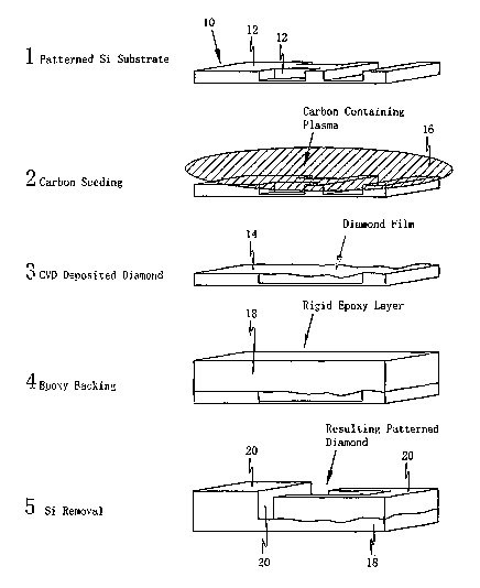
[0015] Figure 1 is an illustration showing the steps of the preferred
embodiment of
the present invention.
DESCRIPTI~II~TT ~F PI~FEI~ED EMS~DIMENTS
[001] In one aspect, the present invention is directed to methods ofmaking
free-
standing, internally-supported, three-dimensional objects having a diamond
layer on at
least a portion of the outer surface of the object. The diamond layer may be
formed by
any method of synthesizing diamond such as high-pressure, high-temperature
(IiPI-IT)
methods or CAD. In accordance with the preferred embodiment of the present
invention,
the diamond is synthesized by CVD.
[0017] In the diamond CVD methods according to the present invention, a
mixture
of hydrogen and carbon-containing gases is activated to obtain a region of gas-
phase non-
equilibl-ium adjacent the substrate on which the diamond will be grown. The
carbon-
containing gas may be selected from a large variety of gases including
methane, aliphatic
and aromatic hydrocarbons, alcohols, ketones, amines, esters, carbon monoxide,
carbon
dioxide, and halogens. Methane is used according to the preferred embodiment
of the
invention.
[0018] The mixture of gases is energized to obtain a region of gas-phase non-
equilibrium adjacent the substrate on which the diamond will be grown. A
variety of gas-
phase activation techniques may be used and these techniques may be
categorized as
3

CA 02515196 2005-08-04
WO 2004/072319 PCT/US2004/003518
either hot-filament CVD, plasma-assisted CVD, or flame CVD. In plasma-assisted
CVD
the plasma may be generated by a number of energy sources including microwave,
radio-
frequency, or direct current electric fields.
[0019] The substrate may be any material suitable for nucleating and growing
diamond such as semiconductor, metal, and insulator materials. Generally, the
nucleation
rates are much higher on carbide forming substrates (e.g., Si, Mo, and ~ than
on
substrates that do not form carbides. According to the preferred embodiment of
the
present invention, silicon substrates are used in view of the desirable
nucleation rates and
well known fabrication techniques of silicon.
[0020] The surface of the substrate on which the diamond will be grown may be
pretreated by ~rarious techniques to enhance diamond nucleation and improve
the
nucleation density of diamond on the surface. Such methods may include (i)
scratching,
abrading, or blasting the surface with diamond particles or paste, (ii)
seeding the surface
with submicron powders such as diamond, silicon, or c~llT, (iii) biasing the
substrate, (iv)
carburi~ation, (v) pulsed laser irradiation, and (vi) ion implantation.
[0021] In accordance with the preferred embodiment of the present invention, a
free-standing, internally-supported, three-dimensional object is provided
having an outer
surface comprising a plurality of intersecting facets wherein at least a sub-
set of the
intersecting facets have a diamond layer of substantially uniform depth. The
teen "facet"
as used herein, includes a surface or face that is either planar or non-
planar.
[0022] Figure 1 illustrates the various steps of the preferred embodiment of
the
present invention. With reference to Figure 1, a silicon substrate 10 is
fabricated using
conventional fabrication techniques to form a mold having an exposed surface
12
defining the sub-set of intersecting facets. A diamond layer 14 of generally
uniform
thickness is grown over the exposed surface 12 of the substrate 10 by any
suitable
method such as hot-filament CVD or plasma-assisted CVD.
4

CA 02515196 2005-08-04
WO 2004/072319 PCT/US2004/003518
[0023] The exposed surface 12 may be pretreated by any suitable technique to
enhance the diamond nucleation and nucleation density on the exposed surface.
Typically, the exposed surface is pretreated by seeding the surface with
carbon atoms 16.
The pretreatment of the exposed surface may be important in order to ensure
growth of
the diamond in the shape of the sub-set of facets which may be relatively
complex.
[0024] In some instances, a backing layer 18 may be formed over at least
portions
of the exposed surface of the newly grown diamond layer to provide structural
support to
the diamond layer when the substrate is removed. Any material that will adhere
to the
exposed diamond and enhance the rigidity of the diamond layer 14 is suitable
for the
backing layer 1 ~ (e.g., epoxy, plastic, viscous polymers that harden, glass,
etc.). The
backing layer may be electrically conductive or non-conductive as desired.
[002] once the backing layer 1 ~ is formed as desired, the substrate 10 is
removed
to expose the surface 20 of the diamond layer 14 grown contiguous to the
substrate which
has been defined by the mold formed by the substrate. The substrate 10 may be
removed
by ally suitable means such as chemical etching. The diamond layer 14 may then
be
treated as desired.
[0026] The free-standing objects made according to the present invention may
find
utility in a variety of applications such as backward wave oscillators, bi-
polar plates for
fuel cells, traveling wave tubes, microchannel plates, and a multitude of
other devices
having a surface comprising a plurality of intersecting facets wherein a sub-
set of
intersecting facets have a diamond layer of substantially uniform thickness.
[0027] While preferred embodiments of the present invention have been
described,
it is to be understood that the embodiments described are illustrative only
and that the
scope of the invention is to be defined solely by the appended claims when
accorded a
full range of equivalence, many variations and modifications naturally
occurring to those
of skill in the art from a perusal hereof.

Representative Drawing
A single figure which represents the drawing illustrating the invention.
Administrative Status

2024-08-01:As part of the Next Generation Patents (NGP) transition, the Canadian Patents Database (CPD) now contains a more detailed Event History, which replicates the Event Log of our new back-office solution.

Please note that "Inactive:" events refers to events no longer in use in our new back-office solution.

For a clearer understanding of the status of the application/patent presented on this page, the site Disclaimer , as well as the definitions for Patent , Event History , Maintenance Fee  and Payment History  should be consulted.

Event History

Description Date
Letter Sent 2010-04-23
Inactive: Office letter 2010-02-15
Letter Sent 2009-10-02
Letter Sent 2009-07-16
Inactive: Office letter 2008-02-13
Inactive: Dead - No reply to Office letter 2007-11-07
Application Not Reinstated by Deadline 2007-11-07
Inactive: Status info is complete as of Log entry date 2007-01-18
Inactive: Abandoned - No reply to Office letter 2006-11-07
Inactive: Cover page published 2005-12-08
Inactive: First IPC assigned 2005-12-07
Inactive: IPC assigned 2005-12-07
Inactive: Courtesy letter - Evidence 2005-10-18
Inactive: Notice - National entry - No RFE 2005-10-12
Application Received - PCT 2005-09-22
National Entry Requirements Determined Compliant 2005-08-04
Application Published (Open to Public Inspection) 2004-08-26

Abandonment History

There is no abandonment history.

Maintenance Fee

The last payment was received on 2007-01-15

Note : If the full payment has not been received on or before the date indicated, a further fee may be required which may be one of the following

  • the reinstatement fee;
  • the late payment fee; or
  • additional fee to reverse deemed expiry.

Please refer to the CIPO Patent Fees web page to see all current fee amounts.

Fee History

Fee Type Anniversary Year Due Date Paid Date
Basic national fee - standard 2005-08-04
MF (application, 2nd anniv.) - standard 02 2006-02-06 2006-01-16
MF (application, 3rd anniv.) - standard 03 2007-02-06 2007-01-15
Owners on Record

Note: Records showing the ownership history in alphabetical order.

Current Owners on Record
GENVAC AEROSPACE CORPORATION
Past Owners on Record
GERALD T. MEARINI
JAMES A., JR. DAYTON
Past Owners that do not appear in the "Owners on Record" listing will appear in other documentation within the application.
Documents

To view selected files, please enter reCAPTCHA code :


To view images, click a link in the Document Description column. To download the documents, select one or more checkboxes in the first column and then click the "Download Selected in PDF format (Zip Archive)" or the "Download Selected as Single PDF" button.

List of published and non-published patent-specific documents on the CPD .

If you have any difficulty accessing content, you can call the Client Service Centre at 1-866-997-1936 or send them an e-mail at CIPO Client Service Centre.


Document
Description 
Date
(yyyy-mm-dd) 
Number of pages   Size of Image (KB) 
Description 2005-08-04 5 307
Claims 2005-08-04 5 176
Drawings 2005-08-04 1 24
Abstract 2005-08-04 2 73
Representative drawing 2005-08-04 1 21
Cover Page 2005-12-08 1 45
Reminder of maintenance fee due 2005-10-12 1 109
Notice of National Entry 2005-10-12 1 192
Request for evidence or missing transfer 2006-08-07 1 101
Courtesy - Abandonment Letter (Office letter) 2006-12-19 1 167
PCT 2005-08-04 1 23
Correspondence 2005-10-12 1 26
Correspondence 2008-02-13 1 23
Correspondence 2009-07-16 1 18
Correspondence 2009-10-02 1 14
Correspondence 2009-08-17 1 24
Correspondence 2010-02-15 1 19
Correspondence 2010-04-23 1 14
Fees 2010-03-15 1 26
Fees 2009-01-16 1 45