Note: Descriptions are shown in the official language in which they were submitted.
CA 02515280 2005-11-04
Chen 34/36-4/5-7/8 1
ADAPTIVE OPTICAL EQUALIZATION FOR CHROMATIC AND/OR
POLARIZATION MODE DISPERSION COMPENSATION AND JOINT
OPTO-ELECTRONIC EQUALIZER ARCHITECTURE
Technical Field
This invention relates to optical transmission systems and, more particularly,
to optical equalization.
Baclt~round of the Inyention
Intersymbol interference (ISI) is a problem commonly encountered in high
speed fiber-optic communication systems. This ISI problem can introduce bit
errors
1 o and thus degrade the system performance and reliability. It is typically
caused by two
major impairment sources: chromatic dispersion (sometimes called group
velocity
dispersion or GVD) and polarization mode dispersion (PMD). Another source of
optical transmission impairments is optical noise.
In a fiber-optic link, a number of optical amplifiers are employed to
strengthen
1 s the optical signal. At the same time, such amplifiers add incoherent
amplified
spontaneous emission (ASE) noise (commonly called optical noise).
Because of the frequency-dependent propagation constant in optical fibers,
different spectral components of a pulse travel at slightly different
velocities, resulting
in pulse broadening in the optical domain. Two parameters are commonly used to
2o characterize first-order and second-order chromatic dispersion (GVD) of a
fiber: a
dispersion parameter, in pslkm/nm, and a dispersion slope parameter, in
ps/km/nmz .
GVD of any order is linear in the optical domain but becomes nonlinear after
square-
law photo-detection in the receiver. Usually chromatic dispersion is static
and can be
effectively compensated by a dispersion compensation module (DClvn comprised
of
25 negative dispersion fibers or other passive components. However, a DCM is
usually
expensive and may add unwanted latency in the optical link that causes a drop
in the
network quality of service (QoS). It is also possible that residual chromatic
dispersion remains even after employing a DCM in the optical ink, and is
desirably
compensated for by an equalizer. Therefore, for the purpose of evaluating the
3o performance of an adaptive equalizer, the first~rder chromatic dispersion
is specified
CA 02515280 2005-11-04
Chen 34/36-4/5-7/8 2
in terms of ps/nm without explicitly specifying the fiber type and
transmission
distance.
Polarization mode dispersion (PMD) is caused by differenttraveling speeds of
two orthogonal polarization modes due to fiber birefringence. Fiber
birefringence
originates from non-circularity of the fiber core and can also be induced by
stress,
bending, vibration, and so on. Thus, PMD is dynamic in nature and drifts
slowly over
time. PMD can be modeled as dispersion along randomly concatenated
birefringent
fiber segments through mode coupling between neighboring sections.
Differential
group delay (DGD) is the parameter used to characterize the PMD-induced pulse
to broadening and may follow a Maxwellian distribution. As a result of this
variability,
the PMD of a fiber is usually characterized by the mean DGD parameter in terms
of
ps/sqrt(lcm). In addition, PMD is frequency-dependent. First-order PMD is the
frequency-independent component of this frequency-dependent PMD. Second~order
(or higher-order) PMD is frequency-dependent and has an effect similar to
chromatic
dispersion on pulse broadening.
To evaluate the performance of an equalizer, the instantaneous DGD is used to
describe the delay between the fast and slow orthogonal polarization modes (in
particular, the principal states of polarization (PSPs) of a fiber). In the
wors~case
scenario, the input power is split equally between these two orthogonal
polari~tion
2o modes, i.e., the power-splitting ratio = 0.5. The performance against the
firs~order
instantaneous DGD (frequency-independent dispersion component) in ps is
essential
in evaluating the effectiveness of a dispersion compensator. Since these two
polarization modes are orthogonal to each other, the photo~urrent I(t) at the
photo-
detector is proportional to the summation of the optical power in each
polarization.
Thus, first-order PMD creates linear ISI at the output of the photo-detector.
Optical equalizers have been used in attempts at compensating for these
impairments. The most common form of these equalizers is a cascaded structure,
which tends to have less flexibility in control of filter parameters.
CA 02515280 2005-11-04
Chen 34/36-4/5-7/8 3
In controlling these optical equalizers, often non-adaptive equalization
approaches are used, but these approaches have proven inadequate. What is
needed in
the art is a better way to compensate for chromatic and/or polarization mode
dispersion.
Summary '
In various embodiments; these and other problems and limitations of prior
known optical equalization arrangements are overcome in applicants' unique
invention by employing a controllable optical FIR filter device to realize an
optical
FIR (finite-impulse-response) filter.
1o In one aspect, the present invention provides an apparatus for use in an
adaptive optical equalizer. In one embodiment, the apparatus includes: (1) a
controllable optical FIR filter having an input and an output, and being
coupled to
receive an incoming optical signal and configured to generate an output
optical signal
by phase modulation and/or amplitude modulation of the received optical
signal, the
controllable optical FIR filter including a plurality of similar optical
signals in a
corresponding plurality of optical paths, each of the parallel optical paths
including an
opto-electronic controller responsive to electronic control signals for
effecting the
phase modulation and/or amplitude modulation of the optical signal being
transported
in the optical path and (2) a control signal generator responsive to an
optical output
zo signal from the output of the controllable optical FIR filter for
generating the
electronic control signals in accordance with predetermined criteria.
In another aspect, the present invention provides a method for use in an
adaptive optical equalizer including a controllable optical FIR filter. In one
embodiment, the method includes: (1) adaptively controlling the controllable
optical
FIR filter to modulate a supplied optical signal to generate an equalized
optical output
signal, (2) converting, in accordance with predetermined first criteria, the
equalized
optical output signal to an electronic signal version, (3) utilizing the
electronic signal
version to generate, in accordance with second predetermined criteria,
amplitude
and/or phase control signals, (4) feeding back the control signals to
adaptively control
the controllable optical FIR filter and (5) employing each control signal to
adjust the
amplitude and/or phase of a corresponding optical signal propagating on a
CA 02515280 2005-11-04
Chen 34/36-4/5-7/8 4
corresponding optical waveguide of a parallel array of waveguides of the
controllable
optical FIR filter.
In yet another aspect, the present invention provides an apparatus for joint
opto-electronic equalization. In one embodiment, the apparatus includes: (1)
an
s optical equalizer having an electrical control input, an optical input, an
optical output
and a state that is fixed by values of a plurality of equalization
coefficients, the control
input configured to set values of the coefFcients in a manner that is
responsive to
electrical signals applied to the control input, (2) an optical intensity
detector
configured to produce an analog electrical output signal in response to the
optical
to output emitting light, the analog electrical signal being representative of
an intensity
of the emitted light and (3) an electronic equalizer configured to receive the
analog
electrical output signal and to produce a stream of digital electrical signals
having
values that are responsive to the received analog electrical signal, the
control input of
the optical and electronic equalizers being connected to receive electrical
signals
t s representative of errors in the digital electrical signals.
In still another aspect, the present invention provides a method of joint opto-
electronic equalization. In one aspect, the method includes: (1) producing an
output
stream of optical signals by passing an input optical signalthrough an optical
equalizer,
(2) producing an electrical signal having a value representative of an
intensity of the
20 output stream of optical signals, (3) passing the electrical signal through
an electronic
equalizer to produce an output stream of digital electrical signals and (4)
setting
equalization coefficients of the optical and electronic equalizers by applying
to the
optical and electronic equalizers a stream of signals with values
representative of
errors in the stream of digital electrical signals.
25 Brief Description of the Drawings
FIG. 1 shows, in simplified block diagram form, one embodiment of the
invention;
CA 02515280 2005-11-04
Chen 34/36-4/5-7/8 5
FIG. 2 shows, in simplified block diagram form, details of a controllable
optical FIR filter that may be employed in the practice of the invention of
the
invention;
FIG. 3 shows, in simplified block diagram form, details of another
embodiment of the invention;
FIG. 4 shows, in simplified block diagram form, details of yet another
embodiment of the invention;
FIG. 5 shows, in simplified block diagram form, details of still another
embodiment of the invention; and
1o FIG. 6 shows, in flow diagram form, a method incorporating a technique
carried out according to the principles of the present invention.
Detailed Description of Embodiments of the Invention
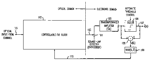
FIG. 1 shows, in simplified block diagram form, one embodiment of the
invention. Specifically, shown is optical input terminal to which an optical
input
signal from an optical channel is supplied. Exemplary optical carrier signals
to be
processed have optical frequencies of about 2.3x10'4 Hertz to about
1.8x10'4Hertz,
i.e., a wavelength of about 1.3 microns to about 1.7 microns. In one example,
an
optical carrier signal having a wavelength of approximately 1.55 microns,
i.e., a
frequency of 1.93 x10'4 Hertz is supplied via input terminal 101 to
controllable
optical FIR filter 102. Also supplied to controllable optical FIR filter 102,
via circuit
path 112, is a control signal, which is used to phase and/or amplitude
modulate, i.e.,
vector modulate the supplied optical signal from input terminal 101 to
generate the
desire optical signal at output terminal 103. The control signal at time, k,
is responsive
to the electrical control signal e(k). The controllable optical FIR filter 102
may, e.g.,
be essentially a controllable optical FIR filter or equalizer. One embodiment
of an
optical FIR filter that may be advantageously employed as controllable optical
FIR
filter 102 in the embodiment of the invention of FIG. 1 is a controllable
optical vector
modulator shown in FIG. 2 and described below. As indicated above, other
embodiments for optical FIR filter 102 may also be equally employed in
practicing
CA 02515280 2005-11-04
Chen 34/36-4/5-7/8 6
the invention. One such embodiment is an array of controllable optical
waveguide
gratings.
For a received optical signal E(t) supplied to controllable optical FIR filter
102
via input terminal 101 the output optical signal Eo (t) from controllable
optical FIR
filter 102 at output terminal 103 is
n n
Eo(t)=~a;e'B'E(t-z;)=~c;E(t-z;), (1)
rm
where n is the number of taps for the optical equalizer, a, is amplitude
parameter, B, and c, = a;eie' is the i'" f Iter coefficient. In one
embodiment, for a tap
delay of 1 / fs , z; = (i -1) l fs for i = 1,..., n. The optical output
signalEo (t) from
controllable optical FIR filter 102 is transported to an optical receiver and
therein to
photodiode 104. As is well known, photodiode 104 is a square-law detector and
generates a current I q(k)I Z in response to detection of Eo (t) , where q(k)
= Eo (k l fs ) .
Transimpedance amplifier 105 converts the current from photodiode 104 to a
voltage
signal, in well known fashion. The electronic voltage signal from
transimpedance
t5 amplifier 105 is supplied to dicer unit 106 and to a negative input of
algebraic adder,
i.e., subtractor 108. An automatic threshold control signal is also supplied
to dicer
unit 106. The threshold control is such as to slice the voltage signal from
transimpedance amplifier 105 in such a manner to realize a desired output
level from
sficer 106. The output from slicer 106 is the desired compensated received
data signal
2o d (k) and is supplied as an output from the receiver and to a positive
input to
algebraic adder 108. The error signal output from subtractor 108 is supplied
to
WUD( a , 9 ) unit 109, where the electronic control signal amplitude (a ) and
phase
( 9 ) values are generated, in accordance with an opto-electronic least-
mean~quare
(OE-LMS) process. The amplitude (a) values and phase (9) values are supplied
via
25 circuit path 110 to adjust the tap coeffcients in controllable optical FIR
filter 102.
Note that although a single electronic feedback path 110 is shown, it will be
understood that as many circuit paths are included equal to the number of
controllable
, CA 02515280 2005-11-04
Chen 34/36-4/5-7/8 7
taps in the FIR filter embodiment of controllable optical FIR filter 102. In
this
example, there may be N such circuit paths. Again, the values of (a ) and ( 9
), in this
embodiment of the invention, are generated in accordance with a single OE-LMS
process. It is further noted that when only the amplitude of the received
optical signal
is modulated only the amplitude adjustment values (a) are supplied from WUD(a,
6) unit 109 to controllable optical FIR filter 102. Similarly, when only the
phase of
the received optical signal is being modulated only the phase adjustment
values (B )
are supplied from unit 109 to controllable optical FIR filter 102. Finally,
when both
the amplitude and phase of the received optical signal are being modulated
both the
amplitude adjustment values (a) and the phase adjustment values (9) are
supplied
from unit 109 to controllable optical FIR filter 102.
Not shown in the above embodiment is the typical clock data recovery
circuitry (CDR).
Just before the CDR, an uncompensated detected signal may contain a certain
amount of ISI induced by optical impairments along the optical path, such as
GVD
and PMD. To remove the ISI present in the electronic signal before recovering
the bit
stream, a coefficient-updating process is employed, in accordance with the
invention,
to control controllable optical FIR filter 102. Operating in the optical
domain, this
process, however, minimizes the electronic error, e(k), between the
compensated
2o signal, d(k), and the desired signal in the mean square sense in a similar
fashion to
the least-mean-square (LMS) algorithm for pure electronic equalization. Thus,
the ISI
elimination process in this invention utilizes a single OE-LMS process.
FIG. 2 shows, in simplified block diagram form, details of an optical vector
modulator that may be utilized as controllable optical FIR filter 102 employed
in FIG.
1 in the embodiment of the invention. The optical vector modulator 102 is
based on
the summing of multiple optical tapped delay lines. The principle of operation
is as
follows: The input optical signal E(t) to be phas~shifted and/or to be
amplitude-
modulated is a modulated optical carrier. Input optical signal E(t) is
supplied to
optical vector modulator 102 via input terminal 101 where it is split via
input
CA 02515280 2005-11-04
Chen 34/36-4/5-7/8 8
multimode interference (MMI) coupler 201 into a plurality of similar branches.
Input
MMI 102 is essentially a power splitter. Each of the plurality of branches is
equipped
with an amplitude and/or phase modulator 202-1 through 202-N to adjust the
amplitude and/or phase of the input optical carrier E(t). In this example, not
to be
construed as limiting the scope of the invention, both the amplitude and phase
is
adjusted in each branch of the optical vector modulator 102. Each of the
amplitude
and phase modulators 202-1 through 202-N is followed by an optical delay line,
namely, delay units 203-1 through 203-N, respectively. The delays T~ through
T" in
each of the modulator branches including phase modulators 202-1 through 202-N
are
generated by delay units 203-1 through 203-N respectively. Each of these delay
lines
in delay units 203-1 through 203-N changes the phase of the sub-carrier of the
optical
signal from amplitude and/or phase modulators 201-1 through 201-N,
respectively, by
a fixed amount. For example, the delay Iine in unit 203-1 provides a delay of
i, delay
unit 203-2 provides a delay of 2i, and delay unit 203-N provides a delay of
Ni.
~5 Typically, a delay i of 1/(N x carrier frequency) is required. In one
embodiment,
delay unit 203-1 supplies a zero (0) delay interval, delay unit 203-2 supplies
a delay
of i and so on until delay unit 203-N supplies a delay of i(N-1). Thus, if the
carrier
frequency is 40 GHz, the delay range should be 0,..., 25 picoseconds (ps).
Delay i
can be equal to one (1) bit period, i.e., T=25 ps for the instance of 40 Gbps.
Therefore, the delay range is 0,..., T(N-1 ). Alternatively, delay i can be a
fraction of a
bit period, for example, T/2=12.5 ps. for 40 Gbps. Thus, for the example that
z = T/2
= 12.5 ps., the delay range is 0,..., (N-1)* 12.5 ps. Another MMI 204 coupler,
which
is for example a power combiner, combines all of the amplitude and phase
adjusted,
and delayed optical signals from all branches to produce a modulated output
optical
signal at output 106, which will interfere constructively or destructively
depending on
the summing optical phases from all tributary branches. Therefore, by
interfering
signals with different carrier phase, the phase and the amplitude of the
carrier of the
summing signal can be set to an arbitrary selected state. These interfered
optical
carriers will produce microwave phasors with prescribed amplitude and phase at
the
remote optical detector, namely, photodiode 104 of FIGS. 1 and 3.
CA 02515280 2005-11-04
Chen 34/36-4/5-7/8 9
The electrically controllable amplitude and phase modulator 202 of each
branch of the optical vector modulator 102 is fabricated, for example, in a
material
system with linear electro-optic effect, as InP, GaAs or LiNb03. The effective
refractive index of an optical waveguide changes in proportion to the
electrical field
s applied perpendicular to this waveguide via control circuit path 110. A high
frequency distributed electrical waveguide is engineered to co-propagate with
the
optical wave with matched propagating velocity to deliver the local control
electrical
field with high modulation bandwidth. The different branches will delay flee
optical
signal by a different length of time. This results in different sub-carrier
phases at the
outputs of these delay lines in units 203. In the combiner 204, these
different output
signals from the various branches interfere coherently with different carrier
phases
due to the different time delays these signals experienced. The carrier of the
signal
after the MMI coupler, i.e., power combiner 204, is the sum of all carriers of
the
signals that interfere coherently.
is FIG. 3 shows, in simplified form, details of another embodiment of the
invention. The embodiment of the invention illustrated in FIG. 3 is similar to
that
shown in FIG. 1 except it specifically employed the optical vector modulator
shown
in FIG. 2 for controllable optical FIR filter 102 of FIG 1. It also employs
interferometer 113 (FIG. 3) for generating a signal employed in the O)rLMS
process.
2o Thus, elements similar to those shown in FIG. 1 have been similarly
numbered and
will not be described again in detail.
Tn the embodiment of FIG. 3 an optical interferometer 113 is supplied via
optical path 111 with the optical signal supplied via input 101 to optical
vector
modulator 102, and via optical path 112 with the output optical signal at
output 103 of
z5 optical vector modulator 102. As is well known, optical interferometer 113
in
response to the supplied optical signals develops optical output signals,
which are
representative of the sum and difference of the supplied optical signals.
These sum
and difference signals are supplied to photodiodes 114 and 115. Photodiodes
114 and
11 S generate electronic signals which are supplied to differential amplifier
116, which
3o generates a correlated signal of the optical vector modulator 102, i.e.,
the optical FIR
CA 02515280 2005-11-04
Chen 34/36-4/5-7/8 10
filter, input signal and output q~(k)r(k+i)signal, as described below in
relation to
Equation (5) which is supplied to WUD(a, 9) unit 109. The "*" denotes the
complex conjugate.
Operation of this embodiment of the invention, is described for an incoming
s optical signal E(t) of a single polarization is sampled at a sampling rate
f, =1 /TJ
equal to or being a multiple of the bit rate fb . When fs = fb , controllable
optical
vector modulator 102 (which is a FIR filter having a plurality of parallel
legs) is
synchronous (SYN). On the other hand, when fs is a multiple of the bit rate
fb,
controllable optical vector modulator 102 is said to be fractionally spaced
(FS).
to Denote the sampled data vector as r (k) _ [r(k+L)..x(k-L)]T , where r(k) =
E(kT )
and the superscript T denote a transpose function. The controllable optical
vector
modulator 102 is a FIR filter with a coefficient vector of a length N = 2L+1
is denoted
as c (k) _ [c-~ (k), ..., c; (k), ...,cL (k )]~ , where the coefficient
indices are rearranged to
i=-L,...,L to center the middle tap of the FIR filter for the sake of "easy"
~5 mathematical manipulation. It should be noted that c(k) is complex in
general. The
output of the FIR filter is then q(k) =cH(k)rH(k) _ ~~ -~c; (k)r(k-i). Here
the
superscript H implies Hermitian conjugate transpose and the superscript T
implies
transpose. Then, photodetector 104 (FIG. l, FIG. 3) converts the optical
output signal
q(k) from controllable optical vector modulator 102 to an electronic signal,
namely,
20 I q(k)I2 = q(k)q~ (k) = c" (k)R(k)c(k) , where R(k) = i~ (k)rH (k) . It can
be shown that
R(k) is a Hermitian matrix and, therefore, can be diagonalized by a unitary
matrix.
Error signal e(k) is generated in conjunction with the output from TIA 105
q(k)I Z and the output from sficer 106 d (k) being supplied to the negative
and positive
inputs, respectively, of algebraic adder, i.e., subtractor 108 (FIG. 1, FIG.
3), namely,
25 e(k) = d (k) - I q(k)i2 . It is noted that d (k) is generated during normal
operation of the
invention and is the desired output. It is further noted that a training
sequence can be
employed to train feedback-controlled optical FIR filter 102 of FIG. 1 and
optical
CA 02515280 2005-11-04
Chen 34/36-4/5-7/8 11
vector modulator 102 of FIG. 3 or any other arrangement that realizes the
desired FIR
filter function.
The OE-LMS process tends to minimize deterministically the cost function
defined here as J(k) = le(k)I2. Therefore, taking a step in the negative
gradient
s direction for minimizing the cost function, the OE-LMS process determines
the
optimized c recursively as follows:
c(k + I) = c(k) - 4 Oc{~ e(k), } , (2)
where /3 is a preset step size and Dc{[e(k)]2} is the gradient of the cost
function. In
this example, Dc{[e(k)]z} = 2e(k)Oc{e(k)} =-2e(k)~c{c" (k)R(k)c(k)} . Since it
Io can be shown that ~c{cH(k)R(k)c(k)}=2R(k)c(k), the OE-LMS process updates
the FIR coefficients in the manner that follows:
c(k + 1) = c (k) + ~3e(k)R(k)c (k) (3)
= c (k) + /3e(k)q' (k)i-(k) . (4)
Thus, the f" FIR filter coefficient is updated as follows:
15 c;(k+1)=c; (k)+/3e(k)q'(k)r(k+i). ($)
The additional product term q' (k) results directly from the square-law
detection via photodetector 104 converting the optical signal output from
controllable
optical FIR filter (optical vector modulator) 102 to an electronic signal. In
other
words, the inner product qt (k)r(k - i) between the un-equalized and equalized
2o signals is used for the adjustment of the coefficients of controllable
optical vector
modulator 102. Alternatively, in equation (3), the sole information required
for
optical equalization is the optical input correlation matrix R, since the FIR
filter
coefficients c are already known. To obtain the correlated signal of q(k) and
r(k-i),
interferometer 113 (FIG. 3) is employed. To this end, the optical input signal
E(t) to
25 and the optical output signal Eo (t) from controllable optical FIR filter
102 (optical
vector modulator (FIG.3)) are supplied to first and second inputs,
respectively, of
optical interferometer 113. In known fashion, optical interferometer 113
generates
CA 02515280 2005-11-04
Chen 34/36-4/5-7/8 12
optical signals at its outputs, which are representative of the sum and
difference of the
supplied optical signals from optical vector modulator 102. These optical sum
and
difference signals are supplied to photodiodes 114 and 115, respectively.
Photodetectors 114 and 115, which are photodiodes, convert the optical output
from
s optical interferometer l 13 to electronic signals. These electronic signals
are supplied
to differential amplifier 116 that generates a difference signal, which is
supplied to
WUD(a, B) 109 for use in generating the amplitude and phase control signals a,
8 ,
respectively, for each leg, i.e., tap, of optical vector modulator 102.
The above discussion assumes a polarized incoming optical signal E(t) and,
to thus, leads to a single-polarization OE-LMS process, which can effectively
mitigate
GVD-induced ISI. However, for the instance of first-order PMD, two orthogonal
polarizations and involved, namely, E,, (t) and E" (t) representing the
optical signals
of vertical and horizontal polarizations, respectively. In consideration of
both the
vertical and horizontal polarizations, the electronic output from photodiode
104 is
t s ~q(k)~Z = ~q~ (k)~2 +~qH (k)~2 ~ where qv (k) _ ~H (k)r~ (k) and qH (k) _
~H (k)rx (k) Wider
the assumption of the controllable optical FIR filter, i.e., optical vector
modulator
102, of FIG. 3, being insensitive to polarization, i.e., c,, = cH = c . Hence,
q(k) = cH (k)[R,, (k) +R" (k)]c(k) and
~c{[e(k)]2}=2e(k)Dc{e(k)}=-4e(k)[R~,(k)+RH(k)]c(k). Thus, the OE-LMS
2o process tap weight-date procedure becomes:
c (k + 1) = c (k) + ~3e(k)[R~, (k) + RH (k)]c (k) (6)
_ ~ (k) '~ ~e(k)[qv (k)rv (k) + qe (k)rH (k)]
In scalar form, the i'" FIR filter tap coefficient is updated as follows:
c; (k + 1) = c; (k) + ~3e(k)[q~ (k)r~ (k - i) + qH (k)rH (k - i)] . (8)
2s If we denote
q(k)=[q~(k)~qH(k)]T~u(k-i)=[rv(k-i)~re(k-i)]T
then,
ci (k + 1) = c; (k) + ~3e(k)qH (k)u(k - i) . (9)
CA 02515280 2005-11-04
Chen 34/36-4/5-7/8 13
Here
q"(k)u(k-1)-Ilq(k)Illlu(k-III ~os(eq,~)~
where Ilqll is the Euclidean norm of q and B9,u is the angle between q and a .
In both equations (5) and (9), the knowledge of the inner product of the input
a and
the equalized q is required for the optimization of the optical FIR filter
coefficients.
Note that once the values for all c, are known, the corresponding values for
a; and Bj
are readily generated, since c; =a;e'B~ , as shown in Equation (1) above.
FIG. 4 shows, in simplified block diagram fonm, details of yet another
embodiment of the invention. The embodiment of the invention illustrated in
FIG. 4
1o is similar to that shown in FIG. 3, but includes a WUD(B,C,F) unit 109 that
performs
both optical and electronic equalization. The embodiment of FIG. 4 includes
both
feedforward and feedback electronic equalizers (401, 402). The embodiment
includes
the interferometer 113, photodiodes 114, 115 and differential amplifier 116,
which
connect to the optical vector modulator 102 and WUD(B,C,F) unit 109 as shown
in
FIG. 3: These elements are left out of FIG. 4 for clarity. Here, elements
similar to
those shown in FIG. 3 have been similarly numbered and will not be described
again
in detail.
In the embodiment of FIG. 4, the optical output signalEo(t) from controllable
optical vector modulator 102 is transported to an optical receiver and therein
to
2o photodiode 104. As is well known, photodiode 104 is a square-law detector
and
generates a current Iq(k)IZ in response to detection of Eo(t) . Transimpedance
amplifier 105 converts the current from photodiode 104 to a voltage signal, in
well
known fashion. The electronic voltage signal from transimpedance amplifier 105
is
supplied to feedforward filter F(x) section 401 which is controlled by
WUD(B,C,F)
2s unit 109. The output of feedforward filter F(x) section 401 is provided via
subtractor
403 to sficer unit 106 and to a negative input of algebraic adder, i.e.,
subtractor 108.
An automatic threshold control signal is also supplied to sficer unit 106. The
threshold control is such as to slice the voltage signal from transimpedance
amplifier
105 in such a manner to realize a desired output level from dicer 106: The
output
CA 02515280 2005-11-04
Chen 34/36-4/5-7/8 14
from dicer 106 is the desired compensated received data signal d (k) and is
supplied
as an output from the receiver and to a positive input to algebraic adder 108.
The
subtractor 108 produces an error signal e(k), which is supplied to WUD(B,C,F)
unit
109, where feedback filter B(x) section signal B, feedforward filter F(x)
section signal
F and the electronic control signal C for the optical vector modulator 102 are
generated utilizing a single OE-LMS process. Signal B and signal F are the
control
inputs for the electronic equalizer. Feedback filter B(x) section 402 receives
signal B,
along with the output of sficer 106 and generates an output signal that is
provided to a
negative input of an algebraic adder, i.e., subtractor 403. The amplitude (a )
values
1o and phase (6) components from WUD(B,C,F) unit I09 are supplied via
electrical
feedback path 110 to adjust the tap coefficients in controllable optical
vector
modulator 102. Note that although a single electrical feedback path 110 is
shown, it
will be understood that as many circuit paths are included equal to the number
of
controllable taps or legs included in controllable optical vector modulator
102. In this
example, there may be N such circuit paths. Again, the values of (a ) and/or (
9 )
components are generated in accordance with a single OE-LMS process. It is
further
noted that when only the amplitude of the received optical signal is modulated
only
the amplitude adjustment value (a) components are supplied from unit 109 to
controllable optical vector modulator 102. - Similarly, when only the phase of
the
2o received optical signal is being modulated only the phase adjustment value
(6 )
components are supplied from unit 109 to controllable optical vector modulator
102.
Finally, when both the amplitude and phase of the received optical signal are
being
modulated both the amplitude adjustment value (a ) components and the phase
adjustment value (B) components are supplied from unit 109 to controllable
optical
vector modulator 102.
FIG. 5 shows, in simplified block diagram form, details of still another
embodiment that produces joint optical and electronic equalization. FIG. 5 is
similar
to FIG. 4, except that feedforward filter F(x) section 401 is absent,
simplifying the
overall architecture. However, as has been discovered, the embodiment of FIG.
5 is
CA 02515280 2005-11-04
Chen 34/36-4/5-7/8 15
still remarkably effective at increasing performance with respect to devices
that do not
perform optical and electronic equalization together.
In the embodiment of FIG. 5, the optical output signalEo(t) from controllable
optical vector modulator 102 is transported to an optical receiver and therein
to
photodiode 104. As is well known, photodiode 104 is a square-law detector and
generates a current I q(k)I Z in response to detection of Eo (t) , i.e., q(k)
= Eo (k l f~ ) .
Transimpedance amplifier 105 converts the current from photodiode 104 to a
voltage
signal, in well known fashion. The electronic voltage signal from
transimpedance
amplifier 105 is supplied to algebraic adder 403 and then to sficer unit 106
and to a
to negative input of algebraic adder, i.e., subtractor 108. An automatic
threshold control
signal is also supplied to sficer unit 106. The threshold control is such as
to slice the
voltage signal from transimpedance amplifier 105 in such a manner to realize a
desired output level from sficer 106. The output from sficer 106 is the
desired
compensated received data signal d (k) and is supplied as an output from the
receiver
~ s and to a positive input to algebraic adder 108. The error signal, e(k),
output from
subtractor 108 is supplied to WUD(B,C) unit 109 where feedback filter B(x)
section
signal B and electronic control signal C (having amplitude (a) and phase (9)
components) are generated utilizing a single O&LMS process. Signal B is the
control
inputs for the electronic equalizer. In the exemplary embodiment, WUD(B,C)
unit
20 109 determines B as follows: B(k+1) = B(k)-ae(k)d(k). In the exemplary
embodiment, WLJD(B,C) unit 109 determines C as follows: C(k+1) -
C(k)+(3e(k)q*(k)r(k). Thus, the WUD(B,C) unit 109 jointly optimizes both the
optical
and electronic equalizers by setting both the C(k) and B(k) coefficients based
on the
same LMS process.
25 Feedback filter B(x) section 402 receives signal B, along with the output
of
sficer 106 and generates an output signal that is provided to a negative input
of
algebraic adder, i.e., subtractor 403. The amplitude (a) values and phase (9)
components from WUD(B,C,F) unit 109 are supplied via electronic feedback path
110 to adjust the tap coefficients in controllable optical vector modulator
102. Note
CA 02515280 2005-11-04
Chen 34/36-4/5-7/8 16
that although a single electronic feedback path 110 is shown, it will be
understood
that as many circuit paths are included equal to the number of controllable
taps or legs
included in controllable optical vector modulator I02. Again, in this example,
there
may be N such circuit paths. The values of (a) and/or (9) components, in this
embodiment of the invention, are again generated in accordance with a single
OE-
LMS process. It is also noted again that when only the amplitude of the
received
optical signal is modulated only the amplitude adjustment value (a) components
are
supplied from unit 109 to controllable optical vector modulator 102.
Similarly, when
only the phase of the received optical signal is being modulated only the
phase
to adjustment value (6) components are supplied from unit 109 to controllable
optical
vector modulator 102. Finally, when both the amplitude and phase of the
received
optical signal are being modulated both the amplitude adjustment value (a )
components and the phase adjustment value (9) components are supplied from
unit
109 to controllable optical vector modulator 102.
As stated above, the signal coming out of feedback filter B(x) section 402 is
subtracted from the post-photodetection electronic signal x(k) (from
photodiode 104).
An uncompensated signal in front of sficer I05 may contain a certain amount of
ISI
induced by optical impairments along the optical path, such as GVD and PMD. To
remove the ISI present in the electronic signal before recovering the bit
stream,
2o OE-LMS is used to control both the O-EQ and the E~EQ in a unified fashion.
This
gains advantages of both equalizer types without causing conflict between
optimization of the O-EQ and the E EQ. In essence, OE~LMS minimizes the
electronic error between the compensated signal and the desired signal in the
mean
square sense, which is compatible with the least-mean-square (LMS) algorithm
conventionally used for electronic equalization.
FIG. 6 shows, in flow diagram form, a method incorporating a technique
carried out according to the principles of the present invention. The method
begins in
start step 610 and proceeds to step 620 wherein input signals pass through an
optical
equalizer. As a result, an output stream of optical signals is produced in
step 630.
3o Then in a step 640, an electrical signal is produced. The electrical signal
has a value
CA 02515280 2005-11-04
Chen 34/36-4/5-7/8 17
representative of an intensity of the output stream of optical signals. Next,
in step
650, the electrical signal is passed through an electronic equalizer to
produce an
output stream of digital electrical signals. Then, in step 660, equalization
coefficients
of the optical and electronic equalizers are set by applying to the optical
and
electronic equalizers a stream of signals with values representative of errors
in the
stream of digital electrical signals. The method ends in end yep 670. Those
skilled in the
pertinent art will understand that although these steps have been set forth
sequentially, they
are advantageously performed concurrently to effect equalization of the input
signals to
yield the output stream of optical signals.
The above-described embodiments are, of course, merely illustrative of the
principles of the invention. Indeed, numerous other methods or apparatus may
be
devised by those skilled in the art without departing from the spirit and
scope of the
invention. Specifically, other arrangements may be equally employed for
realizing
the controllable optical FIR filter.