Note: Descriptions are shown in the official language in which they were submitted.
CA 02515606 2005-08-09
DESCRIPTION
SEALING AGENT FOR PHOTOELECTRIC CONVERSION DEVICE AND
PHOTOELECTRIC CONVERSION DEVICE USING THE SAME
Technical Field
The invention relates to a sealing agent, in particular
to a sealing agent for a photoelectric conversion device, a
photoelectric conversion device obtained by using the sealing
agent and a production method of the photoelectric conversion
device. The invention also relates to a solar cell using the
photoelectric conversion device.
Background Art
While solar cells that are noticed as a clean energy source
have been used for home electricity in recent years, the spread
of the solar cell energy in the home has remained insufficient.
The reasons are rather insufficient performance of the solar
cell itself that renders a module to be of large size, low
productivity of the module, and high price of the solar cell
as a result of the drawbacks above.
The solar cell module is assembled by protecting a
photoelectric conversion device such as monocrystalline
silicon, polycrystalline silicon, amorphous silicon,
gallium-arsenic or copper-indium-selenium with an upper
transparent protective material and lower substrate protective
material, and the photoelectric conversion device and
protective materials are fired with a sealing agent to form a
1
CA 02515606 2005-08-09
package. Accordingly, the sealing agent for the photoelectric
conversion device of the solar cell is required to be excellent
in a) moisture resistance, b) electrical insulation, c) heat
resistance, d) moldability and workability, e) adhesive
strength, f) purity, g) chemical resistance and h) gas-barrier
property.
Today, an ethylene-vinyl acetate copolymer having a high
content of vinyl acetate is used as the sealing agent for the
photoelectric conversion device in the solar cell module from
the viewpoint of flexibility and transparency (see Japanese
Patent Application Laid-Open No. 11-54768). However, since
heat resistance and adhesive property of the copolymer are not
sufficient, an organic peroxide is required to be used together
in order to complete the polymerization reaction. However,
this required two production steps of forming a sheet of the
ethylene-vinyl acetate copolymer containing such additives,
and sealing the photoelectric conversion device using the sheet
obtained. In the sheet production step of this process,
extrusion molding speed cannot be increased since the sheet
should be molded at a low temperature so that the organic
peroxide is not decomposed. On the other hand, the sealing step
of the photoelectric conversion device requires two
time-consumingadhesionstepscomprisingastepfortemporarily
adhering in a laminator in several minutes to more than ten
minutes, and a step for finally adhering in an oven in several
tens of minutes to 1 hour at a temperature high enough for
decomposing the organic peroxide. Although production of the
2
CA 02515606 2005-08-09
solar cell module requires much labor and time as described
above, adhesive property and reliability on moistureresistance
remain not so improved.
Heat resistance is not sufficient when the copolymer or
an ionomer having a low melting point is used (Japanese Patent
Application Laid-Open No. 2000-186114). Such resins are not
preferable since the module may be deformed by a temperature
increase during the use of the photoelectric conversion device,
or excess sealing agent may flow out when the solar cell module
is produced by thermal compression bonding to form flashes. The
stress applied on the seal portion in the production process
has been remarkably increased in accordance with an increased
size of photocells in recent years.
The sealing agent is required to be more reliable in
moisture resistance corresponding to the increased length of
seal lines. In addition, the sealing agent is also required
to be able to equalize the thickness between conductive
substrates used for the photoelectric conversion device from
the view point of narrowing the seal lines, while the sealing
agent is required to be excellent in adhesiveness and
flexibility.
In 1991, a photo (solar) cell using a photoelectric
conversion device named as a dye-sensitized solar cell was
developed by Graetzel (Switzerland). This solar cell, which
is also called as a Graetzel cell, comprises a charge transfer
layer (an electrolyte solution containing a redox substance)
interposed between a thin film substrate, which comprises oxide
3
CA 02515606 2005-08-09
semiconductor particles that is sensitized with a dye and serves
as one electrode on a transparent conductive substrate, and a
substrate, facing the transparent conductive substrate, that
serves as a counter-electrode on which a reducing agent such
as platinum is disposed.
For sealing an electrolyte solution between both
electrodes of the dye-sensitized solar cell, square columns
made of a glass, metal or plastic as sealing solids are bonded
with an epoxy resin or a silicone resin between the electrodes
(see Japanese Patent Application Laid-Open No. 2000-173680).
However, work process becomes complicated in such composite
sealing process. Moreover, water vapor permeability is large
when a silicone resin is used for sealing, and this method is
not suitable for long term sealing of a liquid such as the
electrolyte solution in the dye-sensitized solar cell.
Use of a polyisobutene resin as a sealing agent of the
electrolyte solution for the dye-sensitized solar cell is also
reported (Japanese Patent Application Laid-Open No.
2002-313443). According to this report, a thermosetting resin
is used in primary sealing for bonding both electrodes, and a
UV-curable resin is used in secondary sealing for blocking an
injection port after injecting an electrolyte solution through
the port. However, the resin cannot be sufficiently hardened
since the sealing agent contacts the redox charge transfer layer.
While water vapor permeability of this resin is quite low as
compared with a silicone resin, its ductility is so large that
changes of its property against temperature changes are too
4
CA 02515606 2005-08-09
large. Adhesive strength of the resin at a low temperature is
low with additional drawbacks of poor workability, poor
abrasion resistance and slow elastic recovery to render the
solar cell to have poor durability for long term uses.
As hitherto described, the sealing agents that have been
proposed cannot satisfy all the performances required as a
sealing agent for the photoelectric conversion device,
particularly for the photoelectric conversion device for the
dye-sensitized solar cell. In particular, the conventional
sealing agent has no performance for sealing the redox charge
transfer layer.
Disclosure of Invention
The major object of the invention is to provide a sealing
agent for a photoelectric conversion device that is able to bond
upper and lower conductive substrates at an ambient temperature
in the production process of a solar cell with excellent
adhesive strength and reliable moisture resistance, and a
production method of the photoelectric conversion device using
the sealing agent . The inventors of the invention have found,
through intensive studies for solving the problems as described
above, that a highly reliable photoelectric conversion device
could be obtained by using a sealing agent having a specified
composition. The sealing agent is seldom contaminated with the
electrolyte solution, isexcellent in workability, and promptly
hardened with an active energy beam such as UV light or by heating
at low temperatures with good properties of the cured resin such
J
CA 02515606 2005-08-09
as adhesive strength, reliable moisture resistance and gas
barrierproperty. The invention has been completed through the
studies as described above.
Accordingly, the invention provides:
(1) a sealing agent for a photoelectric conversion device
comprising one or more compounds selected from the group
consisting of a compound having a glycidyl structure, a compound
having a cyclohexene oxide structure, a compound having an
oxetane structure and a compound having a vinyl ether structure,
and a cationic polymerization initiator;
(2) a sealing agent for a photoelectric conversion device
comprising at least two compounds selected from a compound
having a glycidyl structure, a compound having a cyclohexene
oxide structure, a compound having an oxetane structure and a
compound having a vinyl ether structure, and a cationic
polymerization initiator;
(3) the sealing agent for a photoelectric conversion
device according to (1) to (3), wherein the compound having a
glycidyl structure is a bisphenol type epoxy resin;
(4) the sealing agent for a photoelectric conversion
device according to (3) , wherein the bisphenol type epoxy resin
is a bisphenol A type epoxy resin;
(5) the sealing agent for a photoelectric conversion
device according to any one of (1) to (9) further containing
a thermoplastic elastomer in the sealing agent for the
photoelectric conversion device;
(6) the sealing agent for a photoelectric conversion
6
CA 02515606 2005-08-09
device according to (5), wherein the content of the
thermoplastic elastomer is less than 20o by weight;
(7) the sealing agent for a photoelectric conversion
device according to any one of (1) to (6) further containing
a coupling agent in the sealing agent for the photoelectric
conversion device;
(8) the sealing agent for a photoelectric conversion
device according to (7) , wherein the coupling agent is a silane
coupling agent;
(9) the sealing agent for a photoelectric conversion
device according to any one of (1) to (8) further containing
an inorganic filler in the sealing agent for the photoelectric
conversion device;
(10) the sealing agent for a photoelectric conversion
device according to (9) , wherein the inorganic filler is alumina
and/or silica;
(11) the sealing agent for a photoelectric conversion
device according to any one of ( 1 ) to ( 10 ) , wherein the cationic
polymerization initiator is a diaryliodinium salt and/or a
triarylsulfonium salt;
(12) a photoelectric conversion device sealed with the
sealingagentforthephotoelectric conversion device according
to any one of (1) to (11);
(13) a dye-sensitized photoelectric conversion device
sealed with the sealing agent for the photoelectric conversion
device according to any one of (1) to (11);
( 14 ) a solar cell comprising the photoelectric conversion
7
CA 02515606 2005-08-09
device according to (12) or the dye-sensitized photoelectric
conversion device according to (13);
(15) a production method of a photoelectric conversion
device comprising the steps of : disposing a conducive substrate
having a semiconductor-containing layer and a conductive
substrate having a counter-electrode to face to one another at
a specified distance; fixing the substrates with a sealing agent
for a photoelectric conversion device interposed at the
periphery of the substrates; and inserting a charge transfer
layer in a gap between the substrates to obtain a photoelectric
conversion device, wherein the sealing agent according to any
one of (1) to (11) is used as the sealing agent; and
(16) a production method of a photoelectric conversion
device comprising the steps of: disposing a conductive
substrate having a semiconductor-containing layer and a
conductive substrate having a counter-electrode to face to one
another at a specified distance; fixing the periphery of the
substrates with the sealing agent for the photoelectric
conversion device of the invention except an injection port for
injecting a charge transfer layer; injecting the charge
transfer layer through the injection port; and sealing the
injection port with the sealing agent for the photoelectric
conversion device of the invention.
Brief Description of the Drawings
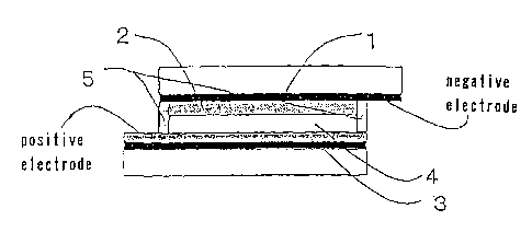
Fig. 1 shows a cross sectional illustration of the main
part of the dye-sensitized solar cell using the photoelectric
8
CA 02515606 2005-08-09
conversion device prepared by using the sealing agent according
to the invention. The reference numeral 1 denotes a conductive
substrate inside of which is conductive, the reference numeral
2 denotes a dye-sensitized semiconductor-containing layer, and
the substrate 1 and semiconductor-containing layer 2 are
collectively named as a semiconductor electrode. The
reference numeral 3 denotes a counter-electrode comprising
platinum and the like disposed on a conductive face at the inside
of a conductive substrate, the reference numeral 4 denotes a
charge transfer layer disposed so as to interpose between the
conductive substrates facing to one another, and reference
numeral 5 denotes a sealing agent.
Fig. 2 is a explanation drawing of a corrosion test of
an ITO electrode, wherein the reference numeral 1 denotes a
glass substrate, the reference numeral 2 denotes an ITO
electrode, and the reference numeral 3 denotes a sealing agent.
Best Mode for Carrying Out the Invention
The invention will be described in detail hereinafter.
The photoelectric conversion device according to the
invention comprises a pairof transparent conductivesubstrates
such as conductive glasses disposed to face to one another with
a given distance apart, and a sealing agent for allowing a charge
transfer layer to interpose between the paired conductive
substrates, wherein a compound having a glycidyl structure such
as a bisphenol type epoxy resin and an alicyclic epoxy resin,
a compound having a cyclohexene oxide structure such as an
9
CA 02515606 2005-08-09
alicyclic epoxy resin, a compound having an oxetane structure
and a compound having a vinyl ether structure, and a cationic
polymerization initiator are used as the sealing agent, in which
a thermoplastic elastomer, a coupling agent and an inorganic
filler, as well as a photosensitizer, an adhesive force
enhancing agent, a spacer ( space controlling material ) , an ion
trapping agent and other additives, if necessary, are mixed and
uniformly dispersed. The viscosity of the sealing agent is
preferably adjusted in order to improve workability depending
on the method for applying the sealing agent (described below) .
The range of the viscosity is, for example, 10,000 to several
hundreds of thousands mPa ~ s, preferably 20, 000 to 100, 000 mPa ~ s
at 25°C as measured by an E-type viscometer. The viscosity may
be adjusted by changing the molecular weight or blend ratio of
the resin used, or by using a viscosity controlling agent or
a solvent.
Each resin or compound constituting the sealing agent of
the invention is preferably of high purity, and commercially
available resins may be used after purification if required.
The method of purification is not particularly limited and
includes conventionally used methods such as washing with water,
distillation, recrystallization, treatment with activated
carbon and column chromatography. Such a purification
facilitates obtaining a highly reliable sealing agent for the
photoelectric conversion device. The sealing agent of the
invention is compatible with a usually used sealing method
comprising the steps of applying the .sealing agent on a
CA 02515606 2005-08-09
conductive substrate by a dispense method or printing method,
bonding both substrates, and hardening the sealing agent by
irradiating an active energy beam.
Hardening of the sealing agent of the invention proceeds
by light irradiation or heating. While the sealing agent can
be hardened by irradiation of an active energy beam such as UV
light to an extent sufficient for practical uses, it is
preferable to further subject the sealing agent to a heat
treatment at a relatively low temperature of 50 to 120°C for
several minutes to 1 hour in order to ensure sufficient
reliability.
Specific examples of the compound having the glycidyl
structure include bisphenol type epoxy resins such as bisphenol
A diglycidyl ether, bisphenol F diglycidyl ether, bisphenol S
diglycidyl ether, brominated bisphenol A diglycidyl ether,
brominated bisphenol F diglycidyl ether, brominated bisphenol
S diglycidyl ether, hydrogenated bisphenol A diglycidyl ether,
hydrogenated bisphenol F diglycidyl ether, hydrogenated
bisphenol S diglycidyl ether, and hydrogenated bisphenol AD
diglycidyl ether; epoxy novolac resins; glycidyl ethers such
as 1,4-butanediol diglycidyl ether, 1,6-hexanediol diglycidyl
ether, glycerin triglycidyl ether, trimethylolpropane
triglycidyl ether, polyethyleneglycol diglycidyl ether and
polypropyleneglycol diglycidyl ether; polyglycidyl ethers of
polyether polyols obtained by addition of one or more alkylene
oxides to an aliphatic polyfunctional alcohol such as
ethyleneglycol, propyleneglycol and glycerin; glycidyl ethers
11
CA 02515606 2005-08-09
of aliphatic higher alcohols; glycidyl ethers of cyclic ethers
such as 1,3-dioxane and 1,4-dioxane; monoglycidyl ethers of
phenol, cresol and butylphenol or polyether alcohols obtained
by addition of an alkylene oxide thereto; glycidyl esters of
higher fatty acids such as epoxidized soybean oil, butyl
epoxystearate, octyl epoxystearate, epoxidized linseed oil and
epoxidized polybutadiene; and phenol novolac epoxy compounds.
Bisphenol type epoxy resins are preferable examples.
Examples of the bisphenol type epoxy resin include
usually produced and commercially available epoxy resins such
as bisphenol A epoxy resin, bisphenol F epoxy resin, bisphenol
S epoxy resin, N,N-diglycidyl-o-touidine, N,N-diglycidyl
aniline, phenyl glycidyl ether, resorcinol diglycidyl ether,
1,6-hexanediol diglycidyl ether, trimethylolpropane
triglycidyl ether, polypropyleneglycol diglycidyl ether, (3,
4-3',4'-epoxycyclo)hexylmethylhexane carboxylate, and
hexahydrophthalic anhydride diglycidyl ester. Examples of
commercially available bisphenol A epoxy resin include Epikote
828, Epikote 10001, Epikote 1004, Epikote 1007, Epikote 1009
and Epikote 1010; examples of commercially available bisphenol
F epoxy resin include Epikote 4001, Epikote 4004 and Epik_ote
4007 (trade names, manufactured by Yuka Shell Epoxy Co. , Ltd. ) ,
YDF-8170, YDF-170, YDF-1755, YDF-2001and YDF-2004 (trade names,
manufactured by Tohto Kasei Co.), RE-310S and RE-4105 (trade
names, manufactured by Nippon Kayaku Co. ) , Epomic 8301 (trade
name, manufactured by Mitsui Petrochemical Co.), and Epicron
8505 (trade name, manufactured by Dainippon Ink & Chemicals,
12
CA 02515606 2005-08-09
Inc. ) ; and examples of commercially available bisphenol F epoxy
resins include RE-3045 and RE-4045 (trade names, manufactured
by Nippon Kayaku Co. ) , Epikote 807 (manufactured by Japan Epoxy
Resins Co., Ltd.), and Adeka Resin EP4900 (trade name,
manufactured by Asahi Denka Co. ) . While the epoxy resins are
not limited to those as described above, bisphenol A epoxy resin
is preferable among them. It is further preferable to use high
purity bisphenol type epoxy resins.
Specific examples of phenol novolac epoxy compounds
include ECN-1273, Araldite ECN-1280 and Araldite ECN-1299
(trade names, manufactured by Asahi Ciba Co.), YDCN-701,
YDCN-702, YDCN-703, YDCN-704 and YDCN-500 (trade names,
manufactured by Tohto Kasei Co.). However, the epoxy resins
are not particularly limited so long as they are compounds
having a glycidyl structure known in the art, and may be
selectively used depending on the desired viscosity of the
sealing agent. These resins may be used alone, or at least two
of them may be used together.
While the bisphenol type epoxy resin available may have
an epoxy equivalent of about 180 to 3,000 g/eq, it is more
preferably about 180 to 900 g/eq. The total amount of chlorine
contained in the epoxy resin used in the invention is preferably
1, 500 ppm or less, more preferably 1, 200 ppm or less, and further
preferably 1, 000 ppm or less . Corrosion of the ITO electrode
of the photocell may be evident when the total content of
chlorine is 1, 500 ppm or more. The epoxy equivalent is measured
by the method according to JIS K7236, and the total content of
13
CA 02515606 2005-08-09
chlorine is measured by a hydrolysis method (the same
hereinafter). The bisphenol type epoxy resin is not limited
to one kind of the resin, and two or more bisphenol epoxy resins
having different epoxy equivalent and molecular weight may be
used together for controlling the viscosity and workability.
A compound having a cyclohexene oxide structure may be
favorably used in the invention. Examples of the compound
having the cyclohexene oxide structure include
3,4-epoxycyclohexylmethyl-3',4'-epoxycyclohexane
carboxylate,
2-(3,4-epoxycyclohexyl-5,5-spiro-3,4-epoxy)cyclohexene-meta
-dioxane, bis(3,4-eoxycyclohexylmehtyl)adipate,
bis(3,4-epoxy-6-methylcyclohexylmethyl)adipate,
vinylcyclohexane oxide, 4-vinylepoxycyclohexane,
3,4-epoxy-6-methylcyclohexyl-3',4'-epoxy-6'-methyl
cyclohexane carboxylate, methylenebis(3,4-epoxycyclohexane),
dicyclopentadiene diepoxide,
di(3,4-epoxycyclohexylmethyl)ether of ethyleneglycol,
ethylenebis(3,4-epoxycyclohexane carboxylate),
lactone-modified 3,4-epoxycyclohexylmethyl
-3',4'-epoxycyclohexane carboxylate, epoxidized tetrabenzyl
alcohol, lactone-modified epoxidized tetrahydrobenzyl alcohol,
and cyclohexane oxide. Examples of the commercially available
compound having the cyclohex_ene oxide structure include
UVR-6100, UVR-6105, UVR-6110, UVR-6128 and UVR-6200 (trade
names, manufactured by Union Carbide Co.); Celoxide 2021,
Celoxide 2021P, Celox.ide 2081, Celoxide 2083, Celoxide 2085,
14
CA 02515606 2005-08-09
Celoxide 2000, Celoxide 3000, Cyclomer A200, Cyclomer M100,
Cyclomer M101, Epolead GT-301, Epolead GT-302, Epolead G01,
Epolead 401, Epolead 403, Epolead HD300 and ETHB (trade names,
manufactured by Daicel Chemical Industries, Ltd. ) ; and KMR-2110
and KMR-2199 (trade names, manufactured by Asahi Kasei Co.).
The compounds are not particularly limited so long as they have
a cyclohexene oxide structure known in the art. The compound
may be selected depending on the desired viscosity of the
sealing agent. One compound may be selected for use, or two
or more of the compounds may be used together.
The compound having the oxetane structure is also
preferably used in the invention. Examples of the compound
having the oxetane structure include trimethylene oxide,
3,3-dimethyl oxetane, 3,3-dichloromethyl oxetane,
3-ethyl-3-methoxymethyl oxetane, 3-ethyl-3-butoxymethyl
oxetane, 3-ethyl-3-hexyloxymethyl oxetane,
3-ethyl-3-hydroxymethyl oxetane, 3-methyl-3-hydroxymethyl
oxetane, 3-ethyl-3-allyloxymethyl oxetane,
3-ethyl-3-(2'-hydroxyethyl)oxymethyl oxetane,
3-ethyl-3-(2'-hydroxy-3'-phenoxypropyl)oxymethyl oxetane,
3-ethyl-3-(2'-hydroxy-3'-butoxypropyl)ox_ymethyl oxetane,
3-ethyl-3-(2'-butoxyethyl)oxymethyl oxetane,
3-ethyl-3-benzyloxymethyl oxetane,
3-ethyl-3-(p-tert-butylbenzyloxymethyl)oxetane,
3-ethyl-3-methacryloyloxymethyl oxetane,
3-ethyl-3-acryloyloxymethyl ox_etane, 3-ethyl-3-phenoxyrnethyl
oxetane, bis(3-ethyl-3-methyloxy)butane,
CA 02515606 2005-08-09
3-chloromethyl-3-methyl oxetane, 3-chloromethyl-3-ethyl
oxetane, 3-bromomethyl-3-methyl oxetane,
3-bromomethyl-3-ethyl oxetane, 3-iodomethyl-3-methyl oxetane,
3-iodomethyl-3-ethyl oxetane, 3-hydroxymethyl-3-ethyl
oxetane, and 1-hydroxy-6-(3-ethyl-3-oxetanylmethoxy)hexyl.
Examples of the commercially available compound having
the oxetane structure include biphenyl dioxetane (BPDO,
manufactured by Ube Industries, Ltd.) and xylylene dioxetane
(XDO, trade name OXT-121, manufactured by Toa Gosei Co. ) . The
compound is not particularly limited so long as all or a part
of oxirane rings of the compound having the glycidyl structure
known in the art are substituted with the oxetane ring. The
compound may be selectively used depending on the desired
viscosity of the sealing agent. One of the compounds may be
used alone, or two or more of them may be used together.
The compound having the vinyl ether structure may be also
favorably used in the invention. Examples of the compound
having the vinyl ether structure include vinyl ether compounds
and propenyl ether compounds.
Examples of the vinyl ether compound include ethyl vinyl
ether, propyl vinyl ether, isobutyl vinyl ether, octadecyl
vinylether, butyl vinylether, ethyleneglycolmonovinylether,
butanediol monovinyl ether, ethyleneglycol butylvinyl ether,
triethyleneglycol methyl vinyl ether, cyclohexanedimethanol
monovinyl ether, cyclohexanedimethanol divinyl ether,
2-ethylhex_yl vinyl ether, t-butyl vinyl ether, t-amyl vinyl
ether, hydroxyethyl vinyl ether, hydroxybutyl vinyl ether,
1F
CA 02515606 2005-08-09
cyclohexyl vinyl ether, butanediol divinyl ether,
ethyleneglycol divinyl ether, diethyleneglycol divinyl ether,
triethyleneglycol divinyl ether, 1,3-butenediol divinyl ether,
neopentylglycol divinyl ether, trimethylolpropane trivinyl
ether, hexanediol divinyl ether, 1,4-cyclohexanediol divinyl
ether, tetraethyleneglycol divinyl ether, pentaerythritol
divinyl ether, pentaerythritol trivinyl ether,
pentaerythritol tetravinyl ether, sorbitol tetravinyl ether,
sorbitol pentavinyl ether, dipentaerythritol hexavinyl ether,
ethyleneglycol diethoxyvinyl ether, triethyleneglycol
diethoxyvinyl ether, ethyleneglycol dipropylenevinyl ether,
trimethylolpropane triethoxyvinyl ether, pentaerythritol
tetraethoxyvinyl ether, dipentaerythritol pentaethoxyvinyl
ether, dipentaerythritol hexaethoxyvinyl ether,
2-hydroxyethyl vinyl ether, 2-hydroxypropyl vinyl ether,
4-hydroxybutyl vinyl ether, pentaerythritol trivinyl ether,
2-ethylhexyl vinyl ether, chloromethyl vinyl ether and
2-chloroethyl vinyl ether.
Examples of the propenyl ether compound include ethyl
propenyl ether, propyl propenylether, isobutylpropenylether,
octadecyl propenyl ether, butyl propenyl ether, ethyleneglycol
monopropenyl ether, butanediol monopropenyl ether,
ethyleneglycol butyl propenyl ether, triethyleneglycol methyl
propenyl ether, cyclohexanedimethanol monopropenyl ether,
cyclohexanedimethanol dipropenyl ether, t-butyl propenyl
ether, t-amyl propenyl ether, hydroxyethyl propenyl ether,
hydroxybutyl propenyl ether, cyclohexyl propenyl ether,
17
CA 02515606 2005-08-09
butanediol dipropenyl ether, ethyleneglycol dipropenyl ether,
diethyleneglycol dipropenyl ether, triethyleneglycol
dipropenyl ether, 1,3-butenediol dipropenyl ether,
neopentylglycol dipropenyl ether, trimethylolpropane
tripropenyl ether, hexanediol dipropenyl ether,
1,4-cyclohexanediol dipropenyl ether, tetraethyleneglycol
dipropenyl ether, pentaerythritol dipropenyl ether,
pentaerythritol tripropenyl ether, pentaerythritol
tetrapropenyl ether, sorbitol tetrapropenyl ether, sorbitol
pentapropenyl ether, dipentaerythritol pentapropenyl ether,
dipentaerythritol hexapropenyl ether, ethyleneglycol
diethoxypropenyl ether, triethyleneglycol diethoxypropenyl
ether, ethyleneglycol dipropylene propenyl ether,
trimethylolpropane triethoxypropenyl ether, pentaerythritol
tetraethoxypropenyl ether, dipentaerythritol panta and
hexaethoxypropenyl ether, tricyclodecane dimethylol propenyl
ether, 2-hydroxyethyl propenyl ether, and 4-hydroxybutyl
propenyl ether. The compounds are not particularly limited so
long as they have the vinyl ether structure known in the art .
The compound may be selectively used depending on the desired
viscosity. The compounds may be used alone, or two or more of
them may be used together. In a preferred embodiment, the
compound having the glycidyl structure, the compound having the
cyclohexene oxide structure and the compound having the oxetane
structure may be mixed for use in the invention.
Each of the compound having the glycidyl structure, the
compound having cyclohexene oxide structure, the compound
18
CA 02515606 2005-08-09
having the oxetane structure and the compound having the vinyl
ether structure may be used alone, or may be used by mixing two
or more of them. When two or more of these compounds are mixed,
the mixture may contain at least one of the compound having the
glycidyl structure, the compound having cyclohexene oxide
structure, the compound having the oxetane structure and the
compound having the vinyl ether structure, and the partner of
combination may be either one of the compounds of the invention
or a compound other than the compounds of the invention. The
mixing ratio differs depending on the desired property of the
sealing agent. These compounds may be purified by an activated
carbon treatment, alumina column treatment or washing with
water after dissolving them in a solvent such as toluene. It
is essential to avoid the solvent from being left behind in the
resin or compound by sufficient drying to completely eliminate
solvent and moisture after purification. The purification
methods are not limited to those as described above, and
molecular distillation may also be employed.
The total content of any one of or a mixture of two or
more of the compounds having the glycidyl structure, having the
cyclohexene oxide structure, having the oxetane structure and
having the vinyl ether structure is usually 5 to 95 o by weight,
preferably 10 to 90o by weight.
Since the viscosity of the resin of the sealing agent for
the photoelectric conversion device is lowered by allowing the
sealing agent for the photoelectric conversion device of the
invention to contain one compound or two or more compounds
19
CA 02515606 2005-08-09
selected from the group consisting of the compounds having the
glycidyl structure, having the cyclohexene oxide structure,
having the oxetane structure and having the vinyl ether
structure when the upper and lower conductive substrates are
bonded in the production process of the photoelectric
conversion device, the substrates can be bonded at an ambient
temperature and a gap between the substrates can be readily
formed.
The sealing agent of the invention is compatible with a
usual bonding method, wherein the sealing agent is applied on
one of the conductive substrates by a dispense method or
printing method, both electrodes are bonded together, and the
sealing agent is hardened by irradiating an active energy beam.
The sealing agent of the invention is also compatible with any
of the following two procedures : the upper and lower conductive
substrates are fixed with the sealing agent of the invention
except a portion that serves as an injection port (primary
sealing), and the injection port is sealed with the sealing
agent of the invention after injecting the charge transfer layer
(secondary sealing); or the upper and lower conductive
substrates are fixed with a sealing agent other than the sealing
agent of the invention except a portion that serves as an
injection port (primary sealing), and the injection port is
sealed with the sealing agent of the invention after injecting
the charge transfer layer (secondary sealing).
While the cationic polymerization initiator used in the
invention is not particularly limited so long as the initiator
CA 02515606 2005-08-09
is able to efficiently generate cations by a heat treatment or
by irradiating an active energy beam, and conventional cationic
polymerization initiators may be used, aromatic opium salts are
favorably used. Examples of the aromatic opium salt comprise
anionic components such as F-, Cl-, Br-, I-, SbF6-, SbF9 , BFq-,
As F6 , PF6 , BC6F5-, BC6H2 (CF3) 2-, N (SOZCF3) 2- and N (CN) 2-, and
aromatic cations containing iodine, sulfur, nitrogen or
phosphorous atoms. A diaryliodonium salt and triarylsulfonium
salt are particularly preferable among them. General examples
of the salts include the compounds represented by the formulae
(1) to (5) below, or those having the same skeletons as the
skeletons in these compounds. The diaryliodonium salts
represented by the formulae (1) and (2) are particularly
preferable among them. While one of these cationic initiators
may be used alone or two or more of them may be used together,
the compound having a high purity is preferably used. The
compound is preferably purified before use when its purity is
low.
21
CA 02515606 2005-08-09
CH3
CH' (1)
CH3
4
H3C(OH2CHZC)2O
4
H3 - R '- ~ (3)
~ % C
CH3
(4)
HOI-3_,CH~ CH~nH
C ( 5)
HOl-i~CH CH~Ol-~
22
CA 02515606 2005-08-09
w
+
/ +'
I
X
H3C \ / + I \ / CI-i3 H3C(HzC)11 ~ ~ + I ~ ~ (CI~i2)11CH3
~i ~i
CH3 + _ ~ CH3 H3C + CH3
H3C I
CH \ , ~ CH3 Ha C ~ CH3
3 :5y
OH H' -- + -
C12H25~H C-
3; ~ _
CH3 _ _ CHaH
I32 I t ! 2
H3C'C~H ~ ~ ~ ~ ~ H C~CH3
1
23
CA 02515606 2005-08-09
'Hs ,r-!-.-\ H~ CHs
Hs ,~~ + : _
HsC H 1. ~~/J'-'~~~~--C~-Il. CHs
X
/ \ ~~ +,~ / \ \ // ~'_ \ /
/ ,-
- x x
~~__~~ /-.:;,
C1 ~, +l~~Wr1 ~~~C(HZC>_u ~I'-~ \ f
\ .l _ \ l~
x
_ _ r ~ -
H3co \ f + ~ \ I \ / ~ \ l
x
o~N ~oz
\ I _' \ l ~ \ l -_" \ l \
x
a
24
CA 02515606 2005-08-09
_ CH3
+S ~ ~ ' ~ cH
3 -
HO ~ ~ +S ~ l OH
CH3
+ ~ ~ ~ -
+S ~ ~ S
I \ / I
/ \
-S ~ ~ S ~ ~ +
x- X
\
I/ \ _
H3c(H~C;hi 0 ,~~ + ~ i
x- X
The content of the cationic polymerization initiator is
usually 0 . 01 to 20 o by weight, preferably 0 . 1 to 10 o by weight,
and more preferably 1 to 7o by weight, in the sealing agent.
The sealing agent for the photoelectric conversion device
of the invention may contain optional components such as a
thermoplastic elastomer, a coupling agent, an inorganic filler,
a photosensitizer and other additives in addition to the
compounds havingthe glycidylstructure, havingthe cyclohexene
CA 02515606 2005-08-09
oxide structure, having the oxetane structure and having the
vinyl ether structure, and the cationic polymerization
initiator.
A SBS block copolymer comprising hydrogenated butadiene
blocks (such as Toughtec M series, manufactured by Asahi Kasei
Co. ) may be preferably used as an example of the thermoplastic
elastomer that may be contained, if necessary, in the invention.
The thermoplastic elastomer that is blended in the epoxy resin
in advance ( for example trade name X-4801, manufactured by Asahi
Kasei Co. ) may be used. Impact resistance and adhesive strength
can be improved by blending such thermoplastic elastomer. The
content of the thermoplastic elastomer is preferably less than
20o by weight in the sealing agent. Excess addition of the
thermoplastic elastomer is not preferable since the viscosity
becomes too high.
Examples of the coupling agent added, if necessary, in
the invention include silane coupling agents such as
3-glycidoxypropyl trimethoxysilane, 3-glycidoxypropylmethyl
dimethoxysilane, 3-glycidoxypropylmethyl dimethoxysilane,
2-(3,4-epoxycyclohexyl)ethyl trimethoxysilane,
N-phenyl-Y-aminopropyl trimethoxysilane,
N-(2-aminoethyl)-3-aminopropylmethyl dimethoxysilane,
N-(2-aminoethyl)-3-aminopropylmethyl trimethoxysilane,
3-aminopropyl triethoxysilane, 3-mercaptopropyl
trimethox_ysilane, vinyl trimethoxysilane,
N-(2-(vinylbenzylamino)ethyl)-3-aminopropyl
trimethoxysilane hydrochloride, 3-methacryloxypropyl
26
CA 02515606 2005-08-09
trimethoxysilane, 3-chloropropylmethyl dimethoxysilane,
3-chloropropyl trimethoxysilane; titanium coupling agents
such as isopropyl(N-ethylaminoethylamino)titanate, isopropyl
triisostearoyl titanate, titanium
di(dioctylpyrophosphate)oxyacetate, tetraisopropyl
di(dioctylphosphite)titanate, and neoalkoxy
tri(p-N-((3-aminoethyl)aminophenyl)titanate; and zirconium or
aluminum coupling agents such as Zr-acetylacetonate,
Zr-methacrylate, Zr-propionate, neoalkoxy zirconate,
neoalkoxy tris(neodecanoyl) zirconate, neoalkoxy
tris(dodecanoyl) benzenesulfonyl zirconate, neoalkoxy
tris(ethylenediaminoethyl)zirconate, neoalkoxy
tris(m-aminophenyl)zirconate, ammonium zirconium carbonate,
A1-acetylacetonate, Al-methacrylate, and A1-propionate.
Silicone coupling agents are preferable, and specific examples
of the preferably used silicone coupling agent include
epoxysilane coupling agents (such as A-186 and A-187
manufactured by Nippon Unicar Co.), and glycidyl ethoxysilane
and glycidyl methoxysilane (3-glycidoxypropyl
trimethoxysilane (KBM 403) manufactured by Shin-Etsu Chemical
Co.). A sealing agent for the photoelectric conversion device
obtained by using the silane coupling agent as described above
is excellent in reliability in moisture resistance without
substantial decrease in adhesive strength by moisture
absorption, and has good adhesivity to the conductive glass.
The content of the silane coupling agent is preferably about
5o by weight in the sealing agent.
27
CA 02515606 2005-08-09
Inorganic fillers used in the invention, if necessary,
are not particularly limited and include those used in
electronic materials such as a sealing agent . Examples of them
include fused silica, crystalline silica, silicon carbide,
silicon nitride, boron nitride, calcium carbonate, magnesium
carbonate, barium sulfate, calcium sulfate, mica, talc, clay,
alumina, titania, magnesium oxide, zirconium oxide, aluminum
hydroxide, magnesium hydroxide, calcium silicate, aluminum
silicate, lithium aluminum silicate, zirconium silicate,
barium titanate, glass fiber, carbon fiber, molybdenum
disulfide and asbestos. Fused silica, crystalline silica,
silicon nitride, boron nitride, calcium carbonate, barium
sulfate, calcium sulfate, mica, talc, clay, alumina, aluminum
hydroxide, calcium silicate and aluminum silicate are
preferable among them. Fused silica, crystalline silica and
alumina are more preferable.
While the shape of the inorganic filler is not
particularly limited including crushed or spherical fine
powders, the inorganic filler is desired to be as pure as
possible. When the purity is low, the inorganic filler is
purified by repeatedly washing with pure water. It is
preferable to perfectly remove moisture by drying with heating.
Two or more of the inorganic fillers may be mixed, and silica
and alumina are preferably used together.
The maximum particle diameter of the inorganic filler
used in the invention, if necessary, is 10 pm or less, preferably
6 pm or less and more preferably 4 dam or less. In particular,
28
CA 02515606 2005-08-09
the maximum diameter is 4 um or less and average particle
diameter is 2 um or less . A gap may not be successfully formed
after bonding the upper and lower conductive substrates in the
production process of the photoconductive conversion device,
when the maximum diameter of the inorganic filler is larger than
um. The inorganic filler having the preferable maximum
diameter is produced, for example, by classifying crushed
fused silica or crystalline silica. Alumina is produced, for
example, by firing aluminum hydroxide, flame hydrolysis of
anhydrous aluminum chloride, or firing ammonium alum, followed
by crushing and classification.
The content of the inorganic filler used in the invention,
if necessary, is preferably less than 30o by weight, more
preferably less than 20o by weight, in the sealing agent for
the photoelectric conversion device. When the content of the
inorganic filler is larger than 60o by weight, a gap for the
photocell can be hardly formed since the sealing agent is
difficult to deform (elongate) because the content of the
inorganic filler is too large.
Other additives such as a photosensitizer, viscosity
controlling agent, adhesiveforce enhancingagent, iontrapping
agent and pigment may be blended, if desired, in the sealing
agent according to the invention in addition to the components
as described above.
While the photosensitizer reported by Crivllo (Adv. in
Polymer Sci . , 62, 1 ( 1984 ) ) is an example, the photosensitizer
is not limited thereto. Any photosensitizer having a
29
CA 02515606 2005-08-09
photosensitizing action may be used, or two or more of such
photosensitizers may be used together. Specific examples of
the photosensitizer available include thioxanthone,
anthracene and pyrene.
Examples of the viscosity controlling agent include a
modified oligomer of butadiene-acrylonitrile copolymer,
novolac type epoxy resin and diallylphthalate resin (for
example, Daiso Dap, manufactured by Daiso Co.). Acrylic
core-shell fine particles (F351, manufactured by Nippon Zeon
Co.) are an example of the adhesive force enhancing agent.
The sealing agent for the photoelectric conversion device
of the invention can be readily obtained by mixing at least one
of a bisphenol type epoxy resin, the compounds having the
glycidyl structure, having the cyclohexene oxide structure,
having the oxetane structure and having the vinyl ether
structure, and a cationic polymerization initiator, and other
additives, if necessary, such as a thermoplastic elastomer, a
coupling agent, an inorganic filler, an adhesive force
enhancing agent, an ion trapping agent, a photosensitizer and
others, and by homogeneously dispersing the mixture. The
viscosity of the sealing agent is preferably adjusted in order
to improve workability depending on the mode of application of
the sealing agent. The viscosity is, for example, usually in
the range of several tens of thousands to several millions mPa ~ s,
preferably in the range of several tens of thousands to several
hundreds of thousands mPa ~ s, as measured by an E-viscometer at
a temperature of 25°C. The viscosity may be controlled by
J V
CA 02515606 2005-08-09
changing the molecular weight and the amount of blending of the
resin used, or by using the viscosity controlling agent or a
solvent.
An example of the ion trapping agent is DHT-6 (trade name,
manufactured by Kyowa Chemical Industry Co.), and titanium
black is an example of the pigment.
The content of the additives as described above is
selected to be in the range of 0 . 1 to 5 o by weight in the sealing
agent.
The sealing agent of the invention is preferably used as
a uniform composition, in which each component is thoroughly
mixed followed by kneading with a three-roll mill for permitting
the composition to be more homogeneous . The sealing agent is
favorably filtered for removing aggregates remaining in the
composition.
A spacer is preferably added for ensuring a desired
thickness of the cell when the sealing agent for the
photoelectric conversion device of the invention is used.
Examples of the spacer include glass fibers and glass beads.
While the diameter of the spacer varies depending on the object,
it is usually 2 to 30 um, preferably 4 to 20 um. The spacer
is used in an amount of 0.1 to 4 parts by weight, preferably
0.5 to 2 parts by weight, and more preferably 0.9 to 1.5 parts
by weight, relative to 100 parts by weight of the sealing agent
for the photoelectric conversion device of the invention.
A solvent may be added for improving workability when the
sealing agent for the photoelectric conversion device of the
31
CA 02515606 2005-08-09
invention is used. Examples of the solvent available include
alcohol solvents, ether solvents, acetate solvents and water.
The solvent may be used alone, or as a mixture of two or more
solvents in an arbitrary ratio.
Examples of the alcohol solvent include alkyl alcohols
such as ethanol and isopropyl alcohol; alkoxy alcohols such as
3-methyl-3-methoxybutanol, 3-methyl-3-ethoxybutanol,
3-methyl-3-n-propoxybutanol, 3-methyl-3-isopropoxybutanol,
3-methyl-3-n-butoxybutanol, 3-methyl-3-isobutoxybutanol,
3-methyl-3-sec-butoxybutanol, and
3-methyl-3-tert-butoxybutanol; and terpineol.
Examples of ether solvents include monohydric alcohol
ether solvents, alkyleneglycol monoalkyl ether solvents,
alkyleneglycol dialkyl ether solvents, dialkyleneglycol alkyl
ether solvents and trialkyleneglycol alkyl ether solvents.
Examples of the monohydric alcohol ether solvent include
3-methyl-3-methoxybutanol methyl ether,
3-methyl-3-ethoxybutanol ethyl ether,
3-methyl-3-n-butoxybutanol ethyl ether,
3-methyl-3-isobutoxybutanol propyl ether,
3-methyl-3-sec-butoxybutanol isopropyl ether, and
3-methyl-3-tert-butoxybutanol n-butyl ether.
Examples of the alkyleneglycol monoalkyl ether include
propyleneglycol monomethyl ether, propyleneglycol monoethyl
ether, propyleneglycol monopropyl ether, propyleneglycol
monoisopropyl ether, propyleneglycol mono-n-butyl ether,
propyleneglycol monoisobutyl ether, propyleneglycol
32
CA 02515606 2005-08-09
mono-sec-butyl ether, propyleneglycol mono-tert-butyl ether,
ethyleneglycol monomethyl ether, ethyleneglycol monoethyl
ether, ethyleneglycol monopropyl ether, ethyleneglycol
monoisopropyl ether, ethyleneglycol mono-n-butyl ether,
ethyleneglycol monoisobutyl ether, ethyleneglycol
mono-sec-butyl ether, and ethyleneglycol mono-tert-butyl
ether.
Examples of the alkyleneglycol dialkyl ether solvents
include propyleneglycol dimethyl ether, propyleneglycol
diethyl ether, propyleneglycol dipropyl ether,
propyleneglycol diisopropyl ether, propyleneglycol di-n-butyl
ether, propyleneglycol diisobutyl ether, propyleneglycol
di-sec-butyl ether, propyleneglycol di-tert-butyl ether,
ethyleneglycol dimethyl ether, ethyleneglycol diethyl ether,
ethyleneglycol dipropyl ether, ethyleneglycol diisopropyl
ether, ethyleneglycol di-n-butyl ether, ethyleneglycol
di-isobutyl ether, ethyleneglycol di-sec-butyl ether, and
ethyleneglycol di-tert-butyl ether.
Examples of the dialkyleneglycol alkyl ether solvents
include dipropyleneglycol methyl ether, dipropyleneglycol
ethyl ether, dipropyleneglycol dipropyl ether,
dipropyleneglycol diisopropyl ether, dipropyleneglycol
di-n-butyl ether, dipropyleneglycol diisobutyl ether,
dipropyleneglycol di-sec-butyl ether, dipropyleneglycol
di-tert-butyl ether, diethyleneglycol dimethyl ether
(diglyme), diethyleneglycol diethyl ether, diethyleneglycol
dipropyl ether, diethyleneglycol diisopropyl ether,
33
CA 02515606 2005-08-09
diethyleneglycol di-n-butyl ether, diethyleneglycol
diisobutyl ether, diethyleneglycol di-sec-butyl ether, and
diethyleneglycol di-tert-butyl ether.
Examples of the trialkyleneglycol alkyl ether solvents
include alkyleneglycol dialkyl ether such as
tripropyleneglycol dimethyl ether, tripropyleneglycol diethyl
ether, tridipropyleneglycol dipropyl ether,
tripropyleneglycol diisopropyl ether, tripropyleneglycol
di-n-butyl ether, tripropyleneglycol diisobutyl ether,
tripropyleneglycol di-sec-butyl ether, tripropyleneglycol
di-tert-butyl ether, triethyleneglycol dimethyl ether,
triethyleneglycol diethyl ether, triethyleneglycol dipropyl
ether, triethyleneglycol diisopropyl ether, triethyleneglycol
di-n-butyl ether, triethyleneglycol diisobutyl ether,
triethyleneglycol di-sec-butyl ether, and triethyleneglycol
di-tert-butyl ether.
Examples of the acetate solvents include alkyleneglycol
monoalkylether acetate suchasethyleneglycolmonomethylether
acetate, ethyleneglycol monoethyl ether acetate,
ethyleneglycol monopropyl ether acetate, ethyleneglycol
monoisopropyl ether acetate, ethyleneglycol mono-n-butyl
ether acetate, ethyleneglycol mono-sec-butyl ether acetate,
ethyleneglycol monoisobutyl ether acetate, ethyleneglycol
mono-tert-butyl ether acetate, propyleneglycol monomethyl
ether acetate, propyleneglycol rrionoethyl ether acetate,
propyleneglycol monoisopropyl ether acetate, propyleneglycol
monopropyl ether acetate, propyleneglycol mono-n-butyl ether
34
CA 02515606 2005-08-09
acetate, propyleneglycol nono-sec-butyl ether acetate,
propyleneglycol monoiobutyl ether acetate, propyleneglycol
mono-tert-butyl ether acetate, 3-methyl-3-methoxybutyl
acetate, 3-methyl-3-ethoxybutyl acetate,
3-methyl-3-propoxybutyl acetate, 3-methyl-3-isopropoxybutyl
acetate, 3-methyl-3-n-butoxyethyl acetate,
3-methyl-3-isobutoxybutyl acetate,
3-methyl-3-sec-butoxybutyl acetate and
3-methyl-3-tert-buroxybutyl acetate; and solvents such as
ethyleneglycol diacetate, diethyleneglycol diacetate,
triethyleneglycol diacetate, propyleneglycol diacetate,
dipropyleneglycol diacetate, tripropyleneglycol diacetate,
diethyleneglycol monobutyl ether acetate, and butyl acetate.
The solvent may be used in an arbitrary quantity necessary
for adjusting the viscosity of the sealing agent for the
photoelectric conversion device so as to be applied with a
dispenser or by screen printing, for example to 200 to 1,000
poise at 25°C. Accordingly, the solvent is used, if necessary,
in a quantity of less than 50 o by weight, preferably less than
30 o by weight, relative to 100 parts by weight of the sealing
agent for the photoelectric conversion device.
The photoelectric conversion device of the invention may
be readily obtained by the steps comprising: applying the
sealing agent of the invention on a conductive surface of the
glass substrate by a dispense method or a printing method;
allowing a pair of the conductive glass substrates to face to
one another; irradiating an active energy beam such as a UV light
CA 02515606 2005-08-09
to the facing glass substrates with compression; and hardening
the sealing agent of the invention. The temperature for
thermosetting is 50 to 200°C with a heating time of several
minutes to several hours . While the active energy beam is not
particularly limited and includes a UV light, X-ray and electron
beam, the UV light is preferably used since a cheap irradiation
apparatus is available for industrial uses. While the light
sources of the UV light include a pressurized mercury lamp, a
high vapor pressure mercury lamp, a metal halide lamp and a xenon
lamp, various light sources may be used without being limited
to those described above. The irradiated luminous energy is
usually 1 to 10, 000 mJ/cm2, preferably l, 000 to 6, 000 mJ/cm2,
and more preferably 2,000 to 4,000 mJ/cm2.
While the sealing agent of the invention is able to exhibit
its performance such as sufficient adhesive strength by itself,
it is favorable to subject it to thermosetting after irradiating
the active energy beam in order to improve long term reliability.
A relatively low heating temperature of 50 to 120°C is
sufficient with a heating time of several minutes to one hour.
Since the cationic polymerization initiator permits hardening
of the resin to proceed by a dark reaction after stopping an
external energy to be supplied and after the initial reaction,
the sealing agent may be hardened by taking advantage of such
property as described above.
The photoelectric conversion device to which the sealing
agent of the invention is applied generally includes all the
devices that are able to convert a light energy to an electric
J CJ
CA 02515606 2005-08-09
energy. A photocell is formed by connecting lead wires so as
to guide an electric current generated from the photoelectric
conversion device to form a closed circuit.
While the sealing agent of the invention is able to use
in variousphotoelectric conversion devices, it isparticularly
suitable for a dye-sensitized solar cell. The dye-sensitized
solar cell comprises a semiconductor electrode and a
counter-electrode, each of which comprises a conductive
substrate, and a charge transfer layer.
The conductive substrate is composed of a conductive
substance represented by FTO (fluorine-doped tin oxide), ATO
(antimony-doped tin oxide) and ITO (indium-doped tin oxide),
which is formed into a thin film on a substrate such as a glass,
plastic or polymer film. Conductivity of the conductive
substrate is usually 1, 000 S2/cm2 or less, preferably 100 S2/cm2
or less.
The semiconductor electrode is obtained by disposing a
semiconductor-containing layer, which is sensitized by
retaining a pigment, on the surface of the conductive substrate
such as the FTO glass.
The semiconductor of the semiconductor-containing layer
is preferably fine particles of metal chalcogenide, and
specific examples thereof include transition metal oxides such
as oxides of Ti, Zn, Sn, lVb, W, In, Zr, Y, La and Ta, oxides
of Al and Si, and perovskite-type oxide such as StTiO-;, CaTiOj
and BaTi03. TiO~, Zn0 and Sn02 are particularly preferal-~le among
them. These oxides may be used as a mixture, and a mixed system
37
CA 02515606 2005-08-09
of Sn02-Zn0 is particularly preferable. The primary particle
diameter is usually 1 to 200 nm, preferably 1 to 50 nm.
The mixed system may be prepared by mixing respective
particles, by mixing as a slurry or paste as will be described
below, or may be overlaid to one another.
The semiconductor-containing layer can be prepared by
directly forming a thin layer of an oxide semiconductor on the
substrate by vacuum deposition, by electrically depositing a
thin film using the substrate as an electrode, and by applying
or coating a slurry or paste on the substrate followed by drying
and hardening or firing. The slurry method is preferable
considering the performance of the oxide semiconductor
electrode. The slurry is obtained by dispersing the fine
particles of the oxide semiconductor as a secondary aggregate
in a dispersion medium using a dispersing agent so that the
average primary particle diameter is 1 to 200 nm, or by
hydrolyzing an alkoxide as a precursor of the oxide
semiconductor by a sol-gel method (see C. J. Barbe, F. Arendse,
P. Compt and M. Graetzel, J. Am. Ceram. Soc., 80, 12, 3157-71
(1997)).
The specific surface area of the fine particles of the
oxide semiconductor obtained as above is usually 1 to 1, 000 m2/g,
preferably 10 to 500 m2/g. Fine particles of the oxide
semiconductorshaving differentparticle diametersmay bemixed
for use. Any dispersion medium may be used for dispersing the
slurry so long as the medium is able to disperse the
semiconductor fine particles, and usually water, and organic
38
CA 02515606 2005-08-09
solvents such as alcohols such as ethanol, ketones such as
acetone and acetylacetone, and hydrocarbons such as hexane may
be used. These solvents may be used as a mixture. Water is
preferably used for reducing viscosity changes of the slurry.
A dispersion stabilizer may be added, if necessary, to
the slurry for obtaining stable primary fine particles.
Examples of the dispersion stabilizer include polyhydric
alcohols such as polyethyleneglycol; alcohol condensates with
phenol or octyl alcohol; cellulose derivatives such as
hydroxypropylmethyl cellulose, hydroxymethyl cellulose,
hydroxyethyl cellulose and carboxymethyl cellulose;
polyacrylamide; poly(meth)acrylic acid and salts thereof;
copolymers of poly(meth)acrylic acid and salts thereof with
acrylamide and (meth)acrylic acid or alkali metal salts
thereof; or water-soluble polyacrylate derivatives as
copolymers of (A) acrylamide and/or alkali metal salts of
(meth)acrylic acid, and (B) (meth)acrylic acid ester such as
methyl (meth)acrylate and ethyl (meth)acrylate or hydrophobic
monomers such as styrene, ethylene and propylene; salts of
melamine sulfonic acid - formaldehyde condensate; salts of
naphthalene sulfonic acid - formaldehyde condensate; salts of
high molecular weight lignin sulfonic acid; acids such as
hydrochloric acid, nitric acid and acetic acid. However, the
dispersion stabilizer is not limited to those as described above.
Any one of these dispersion stabilizers may be used alone, or
two or more of these dispersion stabilizers may be used
together.
39
CA 02515606 2005-08-09
Among these dispersion stabilizers, polyhydric alcohols
such as polyethyleneglycol, condensation products with phenol
or octyl alcohol, and those having carboxylic groups and/or
sulfonic groups and/or amide groups are preferable.
Poly(meth)acrylic acid and salts thereof such as
poly(meth)acrylic acid, sodium poly(meth)acrylate, potassium
poly(meth)acrylate and lithium poly(meth)acrylate,
carboxymethyl cellulose, and acids such as hydrochloric acid,
nitric acid and acetic acid are also preferable.
The concentration of the oxide semiconductor in the
slurry is 1 to 90o by weight, preferably 5 to 80o by weight.
The temperature for firing the substrate on which the
slurry is applied is generally below the melting point
(softening point) of the substrate, usually 100 to 900°C
(melting point or softening point), preferably 100 to 600°C
(melting point or softening point) . While the firing time is
not particularly limited, it is preferably within about 4 hours .
The semiconductor-containing layer may be subjected to
a secondary treatment for improving surface smoothness (see C.
J. Barbe, F. Arendse, P. Compt and M. Graetzel, J. Am. Ceram.
Soc., 80, 12, 3157-71 (1997)). The desired smoothness may be
attained by dipping the entire substrate on which the layer is
formed in a solution of an alkoxide, chloride, nitrate or
sulfide of the same metal as the metal of the semiconductor,
followed by drying or re-firing. Examples of the metal alkoxide
available include titanium ethoxide, titanium isopropoxide,
titanium t-butoxide and n-dibutyl diacetyl tin, and an
CA 02515606 2005-08-09
alcoholic solution thereof is used. Examples of the chloride
include titanium tetrachloride, tin tetrachloride and zinc
chloride, and an aqueous solution thereof is used.
Light energy can be absorbed and converted into an
electric energy by allowing a sensitizing dye to be adsorbed
on the semiconductor-containing layer. The sensitizing dye is
a metal complex dye containing a metal device such as ruthenium
or an organic dye not containing a metal, or a mixture thereof,
and is not particularly limited so long as it is able to sensitize
light absorption.
Then the method for allowing the semiconductor-
containing layer to retain the dye is described.
An example for allowing the semiconductor-containing
layer to retain the dye is to immerse the substrate on which
the semiconductor-containing layer is formed in a solution
obtained by dissolving the dye in a solvent capable of
dissolving the dye, or in a dispersion solution in which the
dye is dispersed when the solubility of the dye is low. The
concentration of the dye in the solution or dispersion solution
may be appropriately determined depending on the respective dye.
The substrate on which the semiconductor-containing layer is
formed is immersed in the solution. The immersing temperature
is generally from ambient temperature to a boiling point of the
solvent, and the immersion time is from 1 hour to 98 hours.
Specific examples of the solvent for dissolving the dye include
methanol, ethanol, acetonitrile, dimethylsulfoxide,
dimethylformamide and 1-butanol. The concentration of the dye
91
CA 02515606 2005-08-09
in the solution is usually 1 x 10⁻⁶ M to 1 M, preferably 1 x
10-5 M to 1 x 10⁻¹ M. The semiconductor electrode is thus obtained
by disposing the semiconductor-containing layer sensitized
with the dye as described above.
One kind of the dye may be retained on the
semiconductor-containing layer, or a plurality of the dyes may
be mixed together. Organic dyes may be mixed, or an organic
dye may be mixed with a metal complex dye . A wide absorption
wavelength region may be utilized by mixing dyes having
different absorption wavelengths to one another to enable a
solar cell having a high conversion efficiency to be obtained.
While the metal complex dye that can be retained is not
particularly limited, phthalocyanine and porphyrin reported by
M. K. Nazeeruddin, A. Kay and M. Graetzel (J. Am. Chem. Soc.,
115, 6382-6390 (1993)) and Shuji Hayase (Mirai Zairyo (Future
Materials) , 13 (1) , 54-59 (2003) ) are preferable, while organic
dyes that can be retained include non-metallic phthalocyanine
and porphyrin as well as cyanine, merocyanine, oxonol and
triphenylmethane dyes, methine dyes such as acrylic acid dyes
reported in WO 2002/011213, and xanthene dyes, azo dyes,
anthraquinone dyes and perylene dyes. Ruthenium complexes and
merocyanine, and methine dyes such as acrylic dyes as described
above are preferable. The proportion of each dye is not
particularly limited when the dyes are used by mixing, and an
optimum condition is selected for each dye. However, it is
generally preferable that the dyes are mixed in an equimolar
arr~ount, or the content of any one of the dye is increased by
92
CA 02515606 2005-08-09
about 10 molo or more. When the dyes are adsorbed on the
semiconductor-containing layer using a solution containing two
or more dissolved or dispersed dyes, the total concentration
of the dyes in the solution may be the same as the concentration
of a dye when only one dye is retained. The solvents as
described above can be used for mixing the dyes, and the solvents
for respective dyes may be the same or different.
It is effective to retain the dyes in the presence of a
clathrate compound for preventing the dyes from associating to
one another, when the dyes are retained on the
semiconductor-containing layer. While examples of the
clathrate compounds include steroid compounds such as cholic
acid, crown ethers, cyclodextrin, calixarene and polyethylene
oxide, cholic acids such as cholic acid, deoxycholic acid,
chenodeoxycholic acid, methyl cholate and sodium cholate, and
polyethylene oxide are preferable. The surface of the
semiconductor electrode may be treated with an amine such as
4-t-butylpyridine after allowing the dye to be retained. For
treating with the amine, the substrate having the
semiconductor-containing layer on which the dye is retained is
immersed in an ethanol solution of the amine.
The solar cell of the invention is usually composed of
the semiconductor electrode comprising a dye retained on the
oxide semiconductor-containing layer, a counter-electrode and
a charge transfer layer. A solution containing a redox
electrolyte or a positive hole transfer material dissolved in
a solvent or a fused salt at an ambient temperature (ionic
93
CA 02515606 2005-08-09
liquid) is used as the charge transfer layer.
While examples of the redox electrolyte used in the solar
cell of the invention include: halogen redox electrolytes
comprising a halogen compound having halogen ions as
counter-ions and halogen molecules; metal redox electrolytes
of metal complexes such as ferrocyanate-ferricyanate,
ferrocene-ferricinium ions and cobalt complexes; and organic
redox electrolytes such as alkylthiol-alkyldisulfide,
viologen dyes and hydroquinone-quinone, the halogen redox
electrolytes are preferable. While iodine molecules and
bromine molecules are examples of the halogen molecules in the
halogen redox electrolyte comprising the halogen
compound-halogen molecule, iodine molecule is preferable.
While examples of the halogen compound comprising halogen ions
as counter-ions include halogenated metal salts such as LiI,
NaI, KI, CsI, CaI2 and CuI, and organic quaternary ammonium salts
of halogens such as tetraalkylammonium iodide, imidazolium
iodide, 1-methyl-3-alkylimidazolium iodide and pyridinium
iodide, salts comprising iodide ions as counter-ions are
preferable. Examples of the salts comprising the iodine ion
as the counter-ion include lithium iodide, sodium iodide and
trimethylammonium iodide.
When the charge transfer layer is composed of a solution
containingthe redox electrolyte, an electricallyinertsolvent
is used for the solvent. Examples of the solvent available
include acetonitrile, propylene carbonate, ethylene carbonate,
3-methoxypropionitrile, methoxyacetonitrile, ethyleneglycol,
49
CA 02515606 2005-08-09
propyleneglycol, diethyleneglycol, triethyleneglycol,
dimethoxyethane, diethyl carbonate, diethyl ether, dimethyl
carbonate, 1,2-dimethoxyethane, dimethylformamide,
dimethylsulfoxide, 1,3-dioxolane, methyl formate, 2-methyl
tetrahydrofuran, 3-methoxyoxaziridine-2-one, Y-butylolactone,
sulfolane, tetrahydrofuran and water, acetonitrile, propylene
carbonate, ethylene carbonate, 3-methoxypropionitrile,
methoxyacetonitrile, ethyleneglycol,
3-methoxyoxaziridine-2-one and Y-butylolactone are
particularly preferable. These solvents may be used alone, or
as a combination of two or more of them. The concentration of
the redox electrolyte is usually 0.01 to 99o by weight,
preferably 0.1 to 90o by weight.
When the charge transfer layer contains a redox
electrolyte, a fused liquid (ionic liquid) at an ambient
temperature is used as a solvent . Examples of the fused liquid
at the ambient temperature include
1-methyl-3-alkylimidazolium iodide, vinylimidazolium
tetrafluoride, 1-ethylimidazole sulfonate, alkylimidazolium
trifluoromethylsulfonyl imide and 1-methylpyrrolidinium
iodide. The viscosity may be increased by dissolving a low
molecular weight gelling agent in the charge transfer layer for
improving durability of the photoelectric conversion device
(see W. Kubo, K. Murakoshi, T. Kitamura, K. Hanabusa, H. Shirai
and S . Yanagida, Chem. Lett . , 1241 ( 1998 ) ) , or a gel electrolyte
can be formed by allowing a reactive component to react after
injecting the charge transfer layer (see Shuji Hayase, Mirai
CA 02515606 2005-08-09
Zairyou (Future Materials), 13(1), 54-59 (2003).
On the other hand, a positive hole transfer material or
P-type semiconductor may be used as a completely solid
electrolyte in place of the redox electrolyte . Examples of the
positive hole transfer material include amine derivatives and
conductive polymers such as polyacetylene, polyaniline and
polythiophene, and a discotic liquid crystal. Examples of the
P-type semiconductor include CuI and CuSCN (see K. Tennakone,
G. K. R. Senadeera, D. B. R. A. De Silva and I. R. M. Kottegoda,
App. Phys. Letter).
The counter-electrode used comprises platinum, carbon,
rhodium or ruthenium, which functions as a catalyst of the redox
reaction of the redox electrolyte, deposited on the surface of
the conductive substrate such as FTO conductive glass, or
precursors of conductive fine particles applied and fired on
the conductive substrate.
The dye-sensitized solar cell using the sealing agent of
the invention comprises: a semiconductor electrode having a
dye-sensitized semiconductor-containing layer on the surface
of the conductive substrate; a counter-electrode disposed so
as to face the semiconductor electrode at a specified distance;
and a charge transfer layer injected into the gap between the
electrodes after sealing the periphery of the semiconductor
electrode and counter-electrode with the sealing agent for the
photoelectric conversion device of the invention. The
semiconductor electrode is formed by disposing the
semiconductor-containing layer sensitized with a dye by taking
46
CA 02515606 2005-08-09
the sealing portion using the sealing agent of the invention
into consideration at around a first conductive substrate. A
spacer such as glass fiber is added to the sealing agent for
the photoelectric conversion device of the invention, and the
sealing agent is applied by screen printing or using a dispenser
so as to leave an injection port of the charge transfer layer
at a part of the periphery of the semiconductor electrode . Then,
the solvent is evaporated off by heating, for example, at 100 °C
for 10 minutes, and another conductive substrate on which a
platinum thin film is disposed is laminated on the first
conductive substrate so that conductive faces of respective
conductive substrates are in opposed relation to one another.
A gap is formed by compression, and the sealing agent hardened
by irradiating a UV light with a high vapor pressure mercury
lamp at a luminous energy of, for example, 3, 000 mJ/cm2 (primary
sealing) . The sealing agent is further hardened by heating at
120°C for 10 minutes. Subsequently, after injecting the charge
transfer layer into the gap between both conductive substrates
through the injection port, the photoelectric conversion device
is obtained by sealing the injection port with the sealing agent
of the invention by the same method as described above
(secondary sealing). The photoelectric conversion device thus
obtained is excellent in durability such as adhesive property,
moisture resistance and heat resistance.
The solar cell of the invention is completed by connecting
lead wires to the positive and negative electrodes of the
photoelectric conversion devicethus obtained, and byinserting
97
CA 02515606 2005-08-09
a resistance between the electrodes.
Examples
The invention will be described in more detail with
reference to examples.
Example 1
A compound having a glycidyl structure [bisphenol A epoxy
resin (RE-301S, manufactured by Nippon Kayaku Co., epoxy
equivalent 182 g/eq, 30 parts by weight; and Epomic 8301,
manufactured by Mitsui Chemical Co. , epoxy equivalent 500 g/eq,
parts by weight)], a compound having a cyclohexene oxide
structure (Celoxide 2021A, manufactured by Daicel Chemical
Industries, Ltd., 30 parts by weight), a compound having an
oxetane structure [BPDO (biphenyl dioxetane), manufactured by
Ube Industries, Ltd. , 30 parts by weight] , and a silane coupling
agent (epoxy silane, Saila Ace 5510, manufactured by Chisso Co. ,
1 part by weight) were thoroughly mixed and heated at 70°C.
After cooling the mixture to room temperature, 3 parts by weight
of diaryliodonium salt (represented by the chemical formula 1,
Rhodorsil Photoinitiator 2074, manufactured by Rhodia Chimie
Co.) as a cationic polymerization initiator and 2 parts by
weight of diethyl thioxanthone (represented by the chemical
formula 6 below, trade name DETX-S, manufactured by Nippon
Kayaku Co. ) as a photosensitizer were added, and were dissolved
by heating at 60°C with stirring in the dark.
48
CA 02515606 2005-08-09
cs>
After dissolution, 1.5 parts by weight of acrylic
core-shell fine particles (trade name F351, manufactured by
Nippon Zeon Co. ) as an adhesive force enhancing agent were added
and mixed with heating at 70°C for 1 hour. Subsequently, 20
parts by weight of synthetic silica (Crystalite 1-FF,
manufactured by Tatsumori Co. ) and 30 parts by weight of alumina
(CR-85, manufactured by Baikowski Japan Co.) were added and
mixed. After kneading in a three-roll mill, the mixture was
filtered under a pressure using a 645 mesh net. The sealing
agent (A) for the photoelectric conversion device of the
invention with a viscosity of about 70,000 Pas was thus
obtained. The viscosity was measured using an E-viscometer at
25°C at a rotation speed of 5 rpm (the same hereinafter).
Example 2
The sealing agent (B) for the photoelectric conversion
device of the invention having a viscosity of about 50, 000 Pa ~ s
was obtained by the same method as in Example l, except that
bisphenol A epoxy resin with an epoxy equivalent of about 250
g/eq and xylylene dioxetane (trade name XDO, manufactured by
Toa Gosei Co.) were used in place of RE-3015 and BPDO,
respectively.
99
CA 02515606 2005-08-09
Example 3
The sealing agent (C) for the photoelectric conversion
device of the invention having a viscosity of about 50, 000 Pa~ s
was obtained by the same method as in Example l, except that
a hydrogenated product of bisphenol A epoxy resin (Adeca Resin
EP 4080, manufactured by Asahi Denka Co. ) was used in place of
Celoxide 2021A.
Example 4
The sealing agent (D) for the photoelectric conversion
device of the invention having a viscosity of about 20, 000 Pa ~ s
was obtained by the same method as in Example 1, except that
the inorganic filler (synthetic silica and alumina) was not
used.
Example 5
The sealing agent (E) for the photoelectric conversion
device of the invention having a viscosity of about 150, 000 Pa ~ s
was obtained by the same method as in Example 2, except that
40 parts by weight of bisphenol A epoxy resin with an epoxy
equivalent of about 400 g/eq was used in place of 30 parts by
weight of RE-3015, and Epomic R-301 was not used.
Example 6
The sealing agent (F) for the photoelectric conversion
device of the invention having a viscosity of about 200, 000 Pa ~ s
was obtained by the same method as in Example 1, except that
the amounts of Epomic 8301 and BPDO were changed to 20 parts
by weight, respectively.
Example 7
CA 02515606 2005-08-09
The sealing agent (G) for the photoelectric conversion
device of the invention having a viscosity of about 150, 000 Pa ~ s
was obtained by the same method as in Example 1, except that
2 parts by weight of an acrylic resin (trade name Dap,
manufactured by Daiso Co.) was added as a viscosity control
agent.
Example 8
The sealing agent (H) for the photoelectric conversion
device of the invention having a viscosity of about 70, 000 Pa ~ s
was obtained by the same method as in Example 1, except that
components (a) to (c) were mixed and purified. The purification
procedure was as follows: a mixed resin of the components was
dissolved in toluene, and washed 5 times with pure water heated
at 60 °C using a separatory funnel. After separating the toluene
phase, 3 o by weight of activated carbon was added to the toluene
phase with stirring at 60 °C. Activated carbon was removed by
filtration, and the toluene phase was concentrated with heating
in vacuum to purify the resin.
Example 9
The sealing agent (I) for the photoelectric conversion
device of the invention having a viscosity of about 70, 000 Pa~ s
was obtained by the same method as in Example 1, except that
the iodonium salt represented by formula (2) was used as the
cationic polymerization initiator in place of the iodonium salt
represented by formula (1).
Example 10
The sealing agent (J) for the photoelectric conversion
51
CA 02515606 2005-08-09
device of the invention having a viscosity of about 200, 000 Pa~ s
was obtained by the same method as in Example 1, except that
the sulfonium salt represented by formula (3) was used as the
cationic polymerization initiator in place of the iodonium salt
represented by formula (1).
Example 11
The sealing agent (K) for the photoelectric conversion
device of the invention having a viscosity of about 300, 000 Pa ~ s
was obtained by the same method as in Example 1, except that
BPDO was changed to PNOX (phenol novolac oxetane compound,
manufactured by Showa Denko Co.), and the sulfonium salt
represented by formula (4) was used as the cationic
polymerization initiator in place of the iodonium salt
represented by formula (1).
Example 12
The sealing agent (Z) for the photoelectric conversion
device of the invention having a viscosity of about 70, 000 Pa ~ s
was obtained by the same method as in Example 1, except that
the amount of the iodonium salt represented by formula (1) as
the cationic polymerization initiator was increased from 3
parts by weight to 7 parts by weight, and the photosensitizer
represented by formula (7) below was used in place of the
photosensitizer DETX-S represented by formula (6),
52
CA 02515606 2005-08-09
CN~CH20CH3
\ \ C2Hs
(7)
CHZCHZOCH3
Example 13
The sealing agent (M) for the photoelectric conversion
device of the invention was obtained by blending 100
parts by weight of a thermoplastic elastomer-containing epoxy
resin (X-4801 (bisphenol A epoxy resin containing 20 o by weight
of Toughtec M20) , manufactured by Asahi Kasei Co. ) as a compound
having a glycidyl structure, 0.5 part by weight of a sulfonium
salt represented by formula (5) as a cationic polymerization
initiator, and 5 parts by weight of an epoxy silane coupling
agent (A-187, manufactured by Nippon Unicar Co.), and mixing
and dispersing the mixture with a three-roll kneader.
Example 14
The sealing agent (N) for the photoelectric conversion
device of the invention was obtained by the same method as in
Example 13, except that 20 parts by weight of a thermoplastic
elastomer-containing epoxy resin (X-4801 (bisphenol A epoxy
resin containing 20o by weight of Toughtec M20), manufactured
by Asahi Kasei Co. ) and 80 parts by weight of bisphenol A epoxy
resin (EP828, manufactured by Shell Co.) as a compound having
a glycidyl structure, were used. The viscosity of the sealing
agent (N) for the photoelectric conversion device was measured
53
CA 02515606 2005-08-09
at 25°C. It was confirmed that the sealing agent had a viscosity
of 50, 000 cps at 20 rpm, which is suitable for screen printing.
Example 15
The sealing agent (0) for the photoelectric conversion
device of the invention was obtained by the same method as in
Example 1, except that a composition prepared by adding 20 parts
by weight of ethyleneglycol divinyl ether (manufactured by BASF
Co. ) as a compound having a vinyl ether structure was added to
the composition in Example 1. The viscosity of the sealing
agent (0) for the photoelectric conversion device was measured
at 25 ° C, and the sealing agent was confirmed to have a viscosity
of 40, 000 cps at 20 rpm, which is suitable for screen printing.
Test Example 1
Glass fiber (1% by weight) with a diameter of 5 um was
added as a spacer to the sealing agent (A) obtained in Example
1. A glass chip with a size of 1.5 mm square was bonded on a
glass substrate, and UV light with a luminous energy of 3, 000
mJ/cm2 was irradiated to the substrate. Glass-glass bonding
shear strength was measured by applying a horizontal load to
the test piece (P) obtained using a bond tester (manufactured
by Seishin Trading Co. ) . A value of the maximum breaking load
divided by the area of the chip was defined to be an ordinary
bonding strength. The result is shown in Table I.
Test Example 2
The ordinary bonding strength was measured by the same
method as in Test Example 1 with respect to a test piece (Q)
obtained by the same method as in Test Example 1 by using the
54
CA 02515606 2005-08-09
sealing agent (M) prepared in Example 13. The result is shown
in Table 1.
Test Example 3
The ordinary bonding strength was measured by the same
method as in Test Example 1 with respect to a test piece (R)
obtained by the same method as in Test Example 1 by using the
sealing agent (N) prepared in Example 14. The result is shown
in Table 1.
Test Example 4
Glass fiber (1o by weight) with a diameter of 5 um was
added as a spacer to the sealing agent (A) obtained in Example
1. A glass chip with a size of 1.5 mm square was bonded on a
glass substrate, and UV light with a luminous energy of 3, 000
mJ/cm2 was irradiated to the substrate, followed by heating at
85°C for 30 minutes for post-hardening. An ordinary bonding
strength was measured by the same method as in Test Example 1
with respect to the test piece (S) obtained. The result is shown
in Table 1.
Test Example 5
The test piece (P) obtained by the same method as in Test
Example 1 was allowed to stand at 121°C for 20 hours under a
pressure using a pressure cooker, and moisture resistant
bonding strength was measured by the same method as in Test
Example 1. The result is shown in Table 1.
Test Example 6
The moisture resistant bonding strength was measured by
the same method as in Test Example 5 with respect to the test
CA 02515606 2005-08-09
piece (P) obtained by the same method as in Test Example 2. The
result is shown in Table 1.
Test Example 7
An ordinary bonding strength of ITO-ITO was measured by
the same method as in Test Example 1, except that the glass
substrate and glass chip in Test Example 1 were changed to ITO
(indium tin oxide) and ITO chip, respectively. The result is
shown in Table 1.
Test Example 8
An ordinary bonding strength of Chromium-ITO was measured
by the same method as in Test Example 1, except that the glass
substrate and glass chip in Test Example 1 were changed to a
chromium substrate and ITO chip, respectively. The result is
shown in Table 1.
Test Example 9
The sealing agent (A) obtained in Example 1 was applied
on a glass substrate on which a PET film was bonded, and the
sealing agent was extended to a thickness of about 0. 1 mm. Then,
the sealing agent was irradiated with UV light with a luminous
energy of 3, 000 mJ/cm2 followed by heating at 90 °C for 30 minutes
to obtain a hardened film. The film was cut into a prescribed
size, and elastic modulus of the film was measured at a heating
rate of 2 °C/min using a thermo-mechanical analyzer (trade name
TMA, manufactured by Rigaku Co.). An expansion coefficient
(a1) was determined from the gradient, and a glass transition
temperature was determined from the inflection point of the
elastic modulus curve. The result is shown in Table 2.
56
CA 02515606 2005-08-09
Test Example 10
The cured film obtained in Test Example 9 was immersed
in boiling water for 5 hours, and water absorption coefficient
(%) was determined from the following equation. The result is
shown in Table 2.
Water absorption coefficient = [(weight after water
absorption - weight before water absorption)/(weight before
water absorption)] x 100
Table 1
Ordinary Bonding Strength Moisture Resistant Bonding
Test Example
(MPa) Strength (MPa)
1 35 -
2 57 -
3 51 -
4 67 -
- 31
6 - 48
7 40 -
8 24 -
Table 2
Expansion Glass Transition Water Absorption
Test Example
Coefficient Temperature ('C) Coefficient (%)
9 2.2 x 10⁻⁵ 131 -
- - 1,2
57
CA 02515606 2005-08-09
Test Example 11
Corrosion test of ITO electrode
A pattern glass was prepared by forming an ITO electrode
film 2 (terminal width of ITO electrode 2mm, gap at the tip 0.1
mm) on a glass substrate 1 as shown in Fig. 2. The sealing agent
(M) obtained in Example 13 was applied on the insulated portion
of the pattern glass, and the sealing agent was hardened by
irradiating UV light by the same irradiation condition as in
Test Example 1. The pattern glass was allowed to stand for 20
days in a constant temperature bath at 65°C and 90o RH while
a direct current voltage of 5 V was applied on the ITO electrode
film. The ITO electrode film at the portion where the adhesive
was applied was observed under a microscope. It was confirmed
from the result that the sealing agent for the photoelectric
conversion device of the invention does not corrode the ITO
electrode film.
Example 16
A paste of Ti02 fine particles (P25, manufactured by
Degussa Co.) as a semiconductor-containing layer was applied
on the conductive surface of a FTO conductive glass substrate
as a conductive substrate of a dye-sensitized solar cell as
shown in an example of the photoelectric conversion device in
Fig. 1. After firing the substrate at 450°C for 30 minutes,
it was immersed in an ethanol solution of a dye (3 x 10⁻⁴ M)
represented by the following formula ( 8 ) for 24 hours to produce
a semiconductor electrode. ~ub.sequently, Pt was deposited on
the conductive surface of another FTO conductive glass
58
CA 02515606 2005-08-09
substrate to prepare a counter-electrode 3.
(8)
Subsequently, the sealing agent (A) 5 prepared in Example
1 was applied at the periphery of the counter-electrode 3 with
a dispenser so as to leave an injection port for the charge
transfer layer 4. After allowing the solvent to evaporate by
heating at 100 ° C for 10 minutes, the semiconductor electrodes
1 and 3 were laminated. After the lamination, a gap was formed
by compression, and both electrodes were bonded together by
hardening the sealing agent by irradiating UV light with a
luminous energy of 3,000 mJ/cm2.
Then, an iodine charge transfer layer 4a [iodine, lithium
iodide, methylhexyl imidazolium iodide (manufactured by
Shikoku Kasei Co.) and t-butylpyridine were adjusted to a
concentration of 0. 1 M, 0. 1 M, 0. 6 M and 1 M, respectively, with
3-methoxy propionitrile] was injected into the cell through the
injection port of the charge transfer layer on the bonded
electrodes. The injection port was sealed with the sealing
59
CA 02515606 2005-08-09
agent of the invention, and the photoelectric conversion device
( 1 ) was obtained by hardening the sealing agent by irradiating
UV light.
Example 17
The photoelectric conversion device (2) was obtained by
the same method as in Example 15, except that the sealing agent
(I) for the photoelectric conversion device in Example 9 was
used in Example 16, and the semiconductor-containing layer was
prepared by hydrolyzing titanium alkoxide by a sol-gel method
according to C. J. Barbe, F. Arendse, P. Compt and M. Graetzel,
J. Am. Ceram. Soc., 80, 12, 3157-71 (1997).
Example 18
The photoelectric conversion device (3) was obtained by
the same method as in Example 16, except that the sealing agent
(J) for the photoelectric conversion device in Example 10 was
used in Example 17, the dye represented by the following formula
(9) was used in place of the dye represented by the chemical
formula (8) , 20 mM of chenodeoxycholic acid was used, and iodine
and tetra-n-propylammonium iodide were adjusted to
concentrations of 0. 05 M and 0.5 M, respectively, with ethylene
carbonate/acetonitrile (6/4) as the charge transfer layer (9b) .
(9)
CA 02515606 2005-08-09
Example 19
The photoelectric conversion device (4) was obtained by
the same method as in Example 16, except that the sealing agent
(L) for the photoelectric conversion device in Example 12 was
used in Example 17.
Example 20
The photoelectric conversion device (5) was obtained by
the same method as in Example 16, except that the sealing agent
(M) for the photoelectric conversion device in Example 13 was
used in Example 17, and a 1:1 mixture of the dye represented
by the formula (8) and a dye represented by the formula (10)
below was used in place of the photosensitizing dye represented
by the formula (8).
( 10)
Example 21
The photoelectric conversion device (6) was obtained by
the same method as in Example 19, except that the sealing agent
(0) for the photoelectric conversion device in Example 15 was
used in Example 20.
Measurement of photoelectric conversion efficiency
61
CA 02515606 2005-08-09
The solar cell of the invention was obtained by connecting
lead wires to the electrodes of each photoelectric conversion
device obtained, and an ammeter and a voltmeter were disposed
to the solar cell. The photoelectric conversion efficiency of
each solar cell was measured as follows. The size of the
effective area of the photoelectric conversion device to be
measured was 0.5 x0.5 cm2. A xenon lamp (1 kW, manufactured
by Ushio Inc. ) was used as a light source, and the output energy
was made 100 mW/cm2 after passing through an AM1.5 filter.
Short circuit current, release current, conversion efficiency
and shape factor were measured using a potentio-galvanostat
(manufactured by Hokuto Denko Co.). The results are shown in
Table 3.
Table 3
Short Circuit Release Photoelectric ConversionShape
Current (mA/cm2)Voltage Efficiency (%) Factor
(V)
Example 12.0 0.70 5.3 0.63
16
Example 17.0 0.75 8.0 0.63
17
Example 14.6 0.72 6.5 0.62
18
Example 17.0 0.75 8.0 0.63
19
Example 17.5 0.75 8.7 0.66
20
Example 17.0 0.73 8.5 0.68
21
Example 12.2 0.70 5.3 0.62
22
Gap-forming test by bonding conductive substrates
To 100 g of the sealing agent for the photoelectric
62
CA 02515606 2005-08-09
conversion device obtained, 1 g of glass fibers with a diameter
of 10 um as spacers are mixed with stirring. This sealing agent
for the photoelectric conversion device is applied on a
conductive substrate (FTO glass substrate) with a size of 50
mm x 50 mm using a dispenser. After allowing the solvent to
evaporate by heating at 100°C for 10 minutes on a hot-plate,
another conductive substrate having the same size as the
substrate prepared above is laminated on the former conductive
substrate at 25°C under a load. Then, the state of the sealing
agent for the photoelectric conversion device is confirmed
whether it is compressed (elongated) to permit the upper and
lower conductive substrates to come into close contact to one
another (lamination test of the conductive substrates). Then,
the laminated conductive substrates having the sealing agent
that has been compressed with a load is clipped, and UV light
is irradiated to the substrates at a luminous energy of 3, 000
mJ/cmz, and the state of the sealing agent for the photoelectric
conversion device between the substrates is confirmed whether
it has been compressed to a thickness of 10 Vim, or to the
thickness as a spacer (gap-forming test of the conductive
substrate). The results are shown in Table 4.
Moisture resistant bonding strength test
To 100 g of the sealing agent for the photoelectric
conversion device obtained, 1 g of glass fibers with a diameter
of 10 um are mixed with stirring as spacers . This sealing agent
for the photoelectric conversion device is applied on a
63
CA 02515606 2005-08-09
conductive substrate (FTO glass substrate) with a size of 50
mm x 50 mm using a dispenser. The solvent is removed by allowing
it to evaporate by heating on a hot-plate, and a glass plate
with a size of 2 mm x 2 mm is bonded on the sealing agent for
the photoelectric conversion device. After hardening the
sealing agent by irradiating UV light with a luminous energy
of 3,000 mJ/cm2 from a high vapor pressure mercury lamp, the
bonded substrate was subjected to a pressure cooker test at 121
°C, 2 atm, and 100%RH to measure shear adhesive strength. The
results are shown in Table 2.
Example
16 17 18 19 20 21
Lamination of Conductive Substrate O O O O O O
Gap Formation between Substrates O O O O O O
Bonding Shear Strength after Humidity Resistance 35 40 43 52 60 51
Test (MPa)
O: Good bonding
D : Gap formation by heating is possible since the sealing agent
for the photoelectric conversion device melts by heating,
although bonding of the conductive substrates is impossible at
ambient temperature.
X : Poor bonding
The magnitude of short circuit current decreases when
impurities are mingled into the charge transfer layer to
64
CA 02515606 2005-08-09
consequently reduce photoelectric conversion efficiency. As
is evident from the photoelectric conversion efficiency in
Table 3, the magnitude in each example is large. Therefore,
it is shown that contaminants are seldom flows into the charge
transfer layer from the sealing agent in the examples. Table
4 shows that bonding between the upper and lower conductive
substrates is possible at ambient temperature in the production
process of the photoelectric conversion device while the
sealing agent has sufficient adhesive strength and reliable
moisture resistance durable to multiple patterning. In
addition, the sealing agent is excellent in flexibility while
hardening is completed within a short period of time to enable
a desired gap to be formed.
Example 22
The photoelectric conversion device (7) was obtained by
the same method as in Example 16, except that the device was
sealed at 110°C within 5 minutes (primary sealing) using
Hymirane (trade name, thermoplastic film with a thickness of
50 Vim, manufactured by Mitsui Dupont Co. ) as a sealing agent.
The results of evaluation of the photoelectric conversion
device (7) obtained are shown in Table 3.
Industrial Applicability
The sealing agent for the photoelectric conversion device
of the invention is hardened with a low luminous energy of about
3, 000 mJ/cm~ in a short period of tune to enable high adhesive
strength to be manifested. The photoelectric conversion
CA 02515606 2005-08-09
device suffers low load by post-heating at a relatively low
temperature for a short period of time. Consequently,
productivity can be markedly improved. The sealing agent of
the invention has a long spot life, excellent workability, high
printability and does not corrode the ITO electrode. The
sealing agent of the invention also has quite good properties
inherently required such as adhesivity, heat resistance and
water absorption coefficient as well as moisture resistant
strength. Therefore, the sealing agent for the photoelectric
conversion device of the invention is quite useful for producing
a photoelectric conversion device having high reliability for
a long period of time.
66