Language selection

Search

Patent 2515614 Summary

Third-party information liability

Some of the information on this Web page has been provided by external sources. The Government of Canada is not responsible for the accuracy, reliability or currency of the information supplied by external sources. Users wishing to rely upon this information should consult directly with the source of the information. Content provided by external sources is not subject to official languages, privacy and accessibility requirements.

Claims and Abstract availability

Any discrepancies in the text and image of the Claims and Abstract are due to differing posting times. Text of the Claims and Abstract are posted:

  • At the time the application is open to public inspection;
  • At the time of issue of the patent (grant).
(12) Patent Application: (11) CA 2515614
(54) English Title: ORGANIC STORAGE COMPONENT AND CORRESPONDING TRIGGERING CIRCUIT
(54) French Title: COMPOSANT ACCUMULATEUR ORGANIQUE ET CIRCUIT DE COMMANDE UTILISE A CET EFFET
Status: Deemed Abandoned and Beyond the Period of Reinstatement - Pending Response to Notice of Disregarded Communication
Bibliographic Data
(51) International Patent Classification (IPC):
  • G11C 13/02 (2006.01)
(72) Inventors :
  • CLEMENS, WOLFGANG (Germany)
  • FIX, WALTER (Germany)
  • GERLT, AXEL (Germany)
  • ULLMANN, ANDREAS (Germany)
(73) Owners :
  • POLYIC GMBH & CO. KG
(71) Applicants :
  • POLYIC GMBH & CO. KG (Germany)
(74) Agent: GOWLING WLG (CANADA) LLP
(74) Associate agent:
(45) Issued:
(86) PCT Filing Date: 2004-01-14
(87) Open to Public Inspection: 2004-08-12
Examination requested: 2005-11-03
Availability of licence: N/A
Dedicated to the Public: N/A
(25) Language of filing: English

Patent Cooperation Treaty (PCT): Yes
(86) PCT Filing Number: PCT/EP2004/000221
(87) International Publication Number: EP2004000221
(85) National Entry: 2005-07-29

(30) Application Priority Data:
Application No. Country/Territory Date
103 03 445.5 (Germany) 2003-01-29

Abstracts

English Abstract


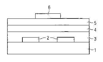
The invention relates to organic storage components and corresponding
triggering circuits. Said organic storage components are provided with a layer
made of a material that is adjustable in a bistable manner or a circuit in
which two OFETs are serially connected. One OFET is connected in parallel to a
capacitor at the low distribution voltage end such that the capacitor is
connected in parallel to the discharging OFET while being charged by the
second OFET.


French Abstract

La présente invention concerne des composants accumulateurs organiques et des circuits de commande utilisés à cet effet. Les composants accumulateurs organiques présentent une couche de matière à deux états stables et comprennent un circuit dans lequel deux OFET sont connectés en série, l'un des OFET étant connecté en parallèle avec un condensateur à savoir sur le côté à tension d'alimentation faible de sorte que le condensateur se trouve connecté en parallèle de l'OFET de décharge et chargé par le second OFET.

Claims

Note: Claims are shown in the official language in which they were submitted.


claims
1. A memory unit comprising at least one organic field effect
transistor (OFET) having at least one substrate, to which
source/drain electrodes (2) embedded in a semi-conductor
layer (4) have been applied, on which an insulator layer
(6) is disposed,
characterized in that
there is present at least on bistably switchable func-
tional layer, of which a property such as the dielectric
constant, electrical conductivity, and/or the magnetic
permeability can be bistably switched.
2. A memory unit as defined in claim 1, wherein said func-
tional layer is the insulator layer (4) of said OFET.
3. A memory unit as defined in claim 1 or claim 2, wherein
the dielectric constant of the bistably switchable
functional layer is switched by application of an elec-
tric potential.
4. A memory unit comprising at least two series-connected
OFETs and a capacitor, wherein said capacitor is con-
nected in parallel with one of said OFETs, this OFET
being the discharge OFET.

Description

Note: Descriptions are shown in the official language in which they were submitted.


CA 02515614 2005-07-29
Description
Organic memory unit and driver circuit therefor
The invention relates to an organic memory unit and a driver
circuit therefor.
Organic-based memory units have been disclosed, for example, in
DE 10045192.6.
For many applications which are based on organic electronics,
organic, write-once or rewritable memories are needed (eg in
RFID tags or in simple electronic games). Above all, non
volatile memories are indispensable for, say, electronic bar
codes or watermarks.
Passive organic memory units are known which are based on
ferroelectric material (Electronic Design, August 20, 2001,
page 56) ("polymeric ferroelectric RAM", inter alia, is pre-
sented in this article). This involves memory-matrix construc-
tional systems which are non-volatile, but also such systems as
are controlled by external circuits, preferably conventional
silicon circuits.
A disadvantage here is the control of the memory units, which
operates by means of an external circuit.
It is therefore an object of the present invention to provide
an organic-based non-volatile memory unit, which is readable
without an external circuit and can be written reversibly.
The present invention relates to an organic-based memory unit
which comprises at least one organic functional layer, in which

CA 02515614 2005-07-29
2
a property (such as the dielectric constant, electrical conduc-
tivity, magnetic permeability) can be switched bistably. The
invention further relates to an organic capacitance memory
which is realized by means of a circuit arrangement including a
capacitor, wherein two OFETs are connected in series and a ca-
pacitor is connected in parallel with one of the OFETs, this
OFET being the discharge OFET.
An organic memory unit comprises at least the following func-
tional layers: lower electrode(s), an insulator, optionally
having integrated storage material, and an upper electrode.
According to one embodiment of the invention, the memory unit
is written simply by increasing the voltage applied to the up
per electrode.
According to another embodiment, the memory unit is integrated
in an organic field effect transistor (OFET).
According to another embodiment, a capacitor assembly serves as
a memory.
For the memory unit, a material is needed in which a certain
property (eg electrical conductivity, dielectric constant or
magnetic permeability) can be switched bistably by external in-
fluences, that is to say, at least two states can be actively
created and these states remain stable in time. Moreover, the
organic memory unit includes a further component by means of
which the state of the bistable material can be read and al-
tered. It is preferred that reading does not alter the state of
the bistable material.

CA 02515614 2005-07-29
3
The invention is described in greater detail below with refer-
ence to three figures, which illustrate embodiments of the in-
vention.
Figure 1 shows a memory which is integrated in an OFET,
Figure 2 shows a capacitor acting as a memory, and
Figure 3 shows a circuit arrangement including a capacitor
acting as a memory.
In Figure 1, an OFET is illustrated diagrammatically in cross-
section and shows a substrate 1, for example a polyester film
to which source/drain electrodes 2 have been applied in struc-
tured form. This can be carried out, for example, by printing
or by means of photolithography. Lower electrodes 2
(source/drain) are embedded in a semiconductor layer 3, which
is covered by an insulator layer 4. These layers can in turn be
applied by printing, knife coating, centrifugal deposition or
spraying. Since some of the materials whose physical properties
such as the dielectric constant, electrical conductivity,
and/or magnetic permeability can be switched bistably also have
insulating properties, the memory can be identical to insulator
layer 4. A layer 5 in the OFET assembly is then unnecessary and
the gate electrode will be connected directly to insulator
layer 4. On the other hand, however, an additional, optionally
very thin layer 5 can also be present, which consists of the
bistably switchable material and which is situated below or
above insulator layer 4. Finally, an upper gate electrode 6 is
disposed either on the insulator layer of bistably switchable
material 4 or on layer 5 attached thereto. The state of the
bistably switchable layer 5 can be read by applying a voltage

CA 02515614 2005-07-29
4
to the source/drain electrodes. The state in layer 5 is pro-
grammed by applying a voltage to gate electrode 6.
Figure 2 shows how a capacitor assembly can be employed as a
memory: dielectric layer 5 having a variable dielectric con-
stant is sandwiched between lower electrode 2 and upper elec-
trode 6. Thus the material having an adjustable dielectric con-
stant in layer 5 lies between two conductive layers - lower
electrode 2 and upper electrode 6, on substrate 1. The dielec-
tric constant can be switched by means of high voltages. The
memory state can then be determined by the charging current of
the capacitor, which is, of course, high or low according to
the dielectric constant.
The material having a switchable dielectric constant used can
be, for example, polyvinylidene dichloride (PVDC) or polyvi-
nylidene difluoride (PVDF). In the case of these materials, the
dielectric constant is switched by high electrical fields.
Figure 3 shows a circuit arrangement having a capacitor acting
as a memory. This organic memory unit or this organic capaci-
tance memory can be realized without special material using the
following circuit: two OFETs 9, 10 are connected in series and
a capacitor, or more precisely, a storage capacitor 11, is con-
nected in parallel with discharge OFET 10. The charge OFET is
designated by 9 and the discharge OFET by 10. The supply volt-
age is applied to 7 and 8. The supply voltage is low at 7 and
the supply voltage is high at 8. Capacitor 11 can be charged by
means of a short impulse to input 13 and discharged by means of
a short impulse to input 12. Input 12 is connected to discharge
OFET 10 and input 13 to charge OFET 9. The state of the memory
can be queried at output 14 of the memory unit, for example by
means of a further OFET.

CA 02515614 2005-07-29
The invention relates to organic memory units and driver
circuits therefor. The organic memory units have a layer of
bistably switchable material or comprise a circuit in which
5 two OFETs are connected in series and one OFET is connected
in parallel with a capacitor on the low potential side
thereof such that the capacitor is connected in parallel
with the discharge OFET and is charged by the second OFET.
The main advantage of the organic memory units presently de-
scribed is that they can be readily included in organic or
polymer-electronic circuits, because they can be easily inte-
grated into the production processes due to their simple con-
struction. The production processes can be readily combined. A
further advantage lies in the simplicity of control of the mem-
ory units, a further important advantage being that the memory
units are non-volatile.

Representative Drawing
A single figure which represents the drawing illustrating the invention.
Administrative Status

2024-08-01:As part of the Next Generation Patents (NGP) transition, the Canadian Patents Database (CPD) now contains a more detailed Event History, which replicates the Event Log of our new back-office solution.

Please note that "Inactive:" events refers to events no longer in use in our new back-office solution.

For a clearer understanding of the status of the application/patent presented on this page, the site Disclaimer , as well as the definitions for Patent , Event History , Maintenance Fee  and Payment History  should be consulted.

Event History

Description Date
Inactive: IPC expired 2023-01-01
Inactive: IPC deactivated 2011-07-29
Time Limit for Reversal Expired 2010-01-14
Application Not Reinstated by Deadline 2010-01-14
Deemed Abandoned - Failure to Respond to Maintenance Fee Notice 2009-01-14
Inactive: IPRP received 2007-03-30
Amendment Received - Voluntary Amendment 2007-02-07
Amendment Received - Voluntary Amendment 2007-01-17
Inactive: IPC from MCD 2006-03-12
Letter Sent 2005-11-23
Letter Sent 2005-11-17
Request for Examination Requirements Determined Compliant 2005-11-03
All Requirements for Examination Determined Compliant 2005-11-03
Request for Examination Received 2005-11-03
Inactive: Single transfer 2005-11-03
Inactive: Courtesy letter - Evidence 2005-11-01
Inactive: Cover page published 2005-10-26
Inactive: Notice - National entry - No RFE 2005-10-24
Correct Applicant Request Received 2005-10-04
Application Received - PCT 2005-09-27
Inactive: IPRP received 2005-07-30
National Entry Requirements Determined Compliant 2005-07-29
Application Published (Open to Public Inspection) 2004-08-12

Abandonment History

Abandonment Date Reason Reinstatement Date
2009-01-14

Maintenance Fee

The last payment was received on 2007-12-11

Note : If the full payment has not been received on or before the date indicated, a further fee may be required which may be one of the following

  • the reinstatement fee;
  • the late payment fee; or
  • additional fee to reverse deemed expiry.

Patent fees are adjusted on the 1st of January every year. The amounts above are the current amounts if received by December 31 of the current year.
Please refer to the CIPO Patent Fees web page to see all current fee amounts.

Fee History

Fee Type Anniversary Year Due Date Paid Date
Basic national fee - standard 2005-07-29
MF (application, 2nd anniv.) - standard 02 2006-01-16 2005-07-29
Registration of a document 2005-11-03
Request for examination - standard 2005-11-03
MF (application, 3rd anniv.) - standard 03 2007-01-15 2006-11-20
MF (application, 4th anniv.) - standard 04 2008-01-14 2007-12-11
Owners on Record

Note: Records showing the ownership history in alphabetical order.

Current Owners on Record
POLYIC GMBH & CO. KG
Past Owners on Record
ANDREAS ULLMANN
AXEL GERLT
WALTER FIX
WOLFGANG CLEMENS
Past Owners that do not appear in the "Owners on Record" listing will appear in other documentation within the application.
Documents

To view selected files, please enter reCAPTCHA code :


To view images, click a link in the Document Description column. To download the documents, select one or more checkboxes in the first column and then click the "Download Selected in PDF format (Zip Archive)" or the "Download Selected as Single PDF" button.

List of published and non-published patent-specific documents on the CPD .

If you have any difficulty accessing content, you can call the Client Service Centre at 1-866-997-1936 or send them an e-mail at CIPO Client Service Centre.


Document
Description 
Date
(yyyy-mm-dd) 
Number of pages   Size of Image (KB) 
Description 2005-07-28 5 172
Representative drawing 2005-07-28 1 4
Claims 2005-07-28 1 25
Drawings 2005-07-28 1 9
Abstract 2005-07-28 1 13
Acknowledgement of Request for Examination 2005-11-16 1 176
Notice of National Entry 2005-10-23 1 192
Courtesy - Certificate of registration (related document(s)) 2005-11-22 1 106
Courtesy - Abandonment Letter (Maintenance Fee) 2009-03-10 1 173
PCT 2005-07-28 18 603
Correspondence 2005-10-03 1 44
PCT 2005-07-29 10 413
PCT 2005-07-28 1 42
Correspondence 2005-10-23 1 27
PCT 2007-03-29 9 265