Note: Descriptions are shown in the official language in which they were submitted.
CA 02515831 2009!09-11
BROADBAND HIGH-FREQUENCY SLIP RING SYSTEM
[0001]
BACKGROUND OF THE INVENTION
[0002] The present invention is generally directed to a contact-type slip ring
system that is
utilized to transfer signals from a stationary reference frame to a moving
reference frame
and, more specifically, to a contact-type slip ring system that is suitable
for high data rate
communication.
[0003] Contact-type slip rings have been widely used to transmit signals
between two
frames that move in rotational relation to each other. Prior art slip rings of
this nature
have utilized precious alloy conductive probes to make contact with a rotating
ring system.
These probes have traditionally been constructed using round-wire, composite
materials,
button contacts or multi-filament conductive fiber brushes. The corresponding
concentric
contact rings of the slip ring are typically shaped to provide a cross-section
shape
appropriate for the sliding contact. Typical ring shapes have included V-
grooves, U-
grooves and flat rings. Similar schemes have been used with systems that
exhibit
translational motion rather than rotary motion.
[0004] When transmitting high-frequency signals through slip rings, a major
limiting
factor to the maximum transmission rate is distortion of the waveforms due to
reflections
from impedance discontinuities. Impedance discontinuities can occur throughout
the slip
ring wherever different forms of transmission lines interconnect and have
different surge
impedances. Significant impedance mismatches often occur where transmission
lines
interconnect a slip ring to an external interface, at the brush contact
structures and where
the transmission lines connect those brush contact structures to their
external interfaces.
Severe distortion to high-frequency signals can occur from either of those
impedance
mismatched transitions of the transmission lines. Further, severe distortion
can also occur
due to phase errors from multiple parallel brush connections.
[0005] The loss of energy through slip rings increases with frequency due to a
variety of
effects, such as multiple reflections from impedance mismatches, circuit
resonance,
-1-
CA 02515831 2005-08-11
WO 2004/075421 PCT/US2004/004613
distributed inductance and capacitance, dielectric losses and skin effect.
High-frequency
analog and digital communications across rotary interfaces have also been
achieved or
proposed by other techniques, such as fiber optic interfaces, capacitive
coupling, inductive
coupling and direct transmission of electromagnetic radiation across an
intervening space.
However, systems employing these techniques tend to be relatively expensive.
[0006] What is needed is a slip ring system that addresses the above-
referenced problems,
while providing a readily producible, economical slip ring system.
SUMMARY OF THE INVENTION
[0007] An embodiment of the present invention is directed to a contacting
probe system
that includes at least one flat brush contact and a printed circuit board
(PCB). The PCB
includes a feedline for coupling the flat brush contact to an external
interface. The flat
brush contact is located on a first side of the PCB and the PCB includes a
plated through
eyelet that interconnects the flat brush contact to the feedline.
[0008] According to another embodiment of the present invention, a contacting
ring
system includes first and second dielectric materials with first and second
sides. The first
dielectric material includes a plurality of concentric spaced conductive rings
located on its
first side and first and second conductive feedlines located on its second
side. A first side
of the second dielectric material is attached to the second side of the first
dielectric
material and a ground plane is located on the second side of the second
dielectric material.
The first feedline is coupled to a first one of the plurality of concentric
spaced conductive
rings, through a first conductive via, and the second feedline is coupled to a
second one of
the plurality of concentric spaced conductive rings, through a second
conductive via. A
groove may be formed in the first dielectric material between the first and
second ones of
the plurality of concentric spaced conductive rings.
[0009] These and other features, advantages and objects of the present
invention will be
further understood and appreciated by those skilled in the art by reference to
the following
specification, claims and appended drawings.
BRIEF DESCRIPTION OF THE DRAWINGS
[0010] In the drawings:
-2-
CA 02515831 2005-08-11
WO 2004/075421 PCT/US2004/004613
[0011] Fig. 1 is a front view of a high-frequency (HF) printed circuit board
(PCB) slip
ring platter including flexible circuit transmission lines that provide
outside connection to
ring structures of the slip ring platter;
[0012] Fig. 2 is a partial perspective view of a plurality of bifurcated flat
brush contacts
and an associated PCB;
[0013] Fig. 3 is a partial view of an exemplary six-finger interdigitated flat
brush contact;
[0014] Fig. 4 is a perspective view of ends of a plurality of bifurcated flat
brush contacts
that are in contact with conductive rings of a PCB slip ring platter;
[0015] Fig. 5 is a partial cross-sectional view of a central eyelet feedpoint
of the bifurcated
flat brush contacts of Fig. 2;
[0016] Fig. 6 is a partial top view of a slip ring system showing the
alignment of a
plurality of bifurcated flat brush contacts, through central eyelet
feedpoints, with
conductive rings of a PCB slip ring platter;
[0017] Fig. 7A shows an electrical diagram of a differential brush contact
system;
[0018] Fig. 7B shows a cross-sectional view of a PCB implementing the
differential brush
contact system of Fig. 7A;
[0019] Fig. 8 is an electrical diagram of a parallel feed differential brush
contact system;
[0020] Fig. 9 is a diagram of a tapered parallel differential transmission
line;
[0021] Fig. 10 is an electrical diagram of a pair of differential gradated
transmission lines;
[0022] Fig. 11 is a perspective view of a portion of a microstrip contact;
[0023] Fig. 12 is a perspective view of the microstrip contact of Fig. 11 in
contact with a
pair of concentric rings of a PCB slip ring platter;
[0024] Fig. 13A is an electrical diagram of a PCB slip ring platter that
implements
differential transmission lines;
[0025] Fig. 13B is a partial cross-sectional view of a three layer PCB
utilized in the
construction of the PCB slip ring platter of Fig. 13A;
[0026] Fig. 14 is an electrical diagram of a PCB slip ring platter that
implements
differential transmission lines;
[0027] Fig. 15 is a partial cross-sectional view of a four layer PCB utilized
in the
construction of the PCB slip ring platter of Fig. 14;
[0028] Fig. 16 is a perspective view of a rotary shaft for receiving a
plurality of PCB slip
ring platters; and
-3-
CA 02515831 2005-08-11
WO 2004/075421 PCT/US2004/004613
[0029] Fig. 17 is a perspective view of the rotary shaft of Fig. 16 including
at least one
slip ring platter mounted thereto.
DETAILED DESCRIPTION OF PREFERRED EMBODIMENTS
[0030] As is disclosed herein, a broadband contacting slip ring system is
designed for
high-speed data transmission over a frequency range from DC to several GHz.
Embodiments of the present invention employ a conductive printed circuit board
(PCB)
slip ring platter that utilizes high-frequency materials and techniques and an
associated
transmission line that interconnects conductive rings of the PCB slip ring
platter to an
external interface. Embodiments of the present invention may also include a
contacting
probe system that also utilizes PCB construction and high-frequency techniques
to
minimize degradation of signals attributable to high-frequency and surge
impedance
effects. The contacting probe system includes a transmission line that
interconnects the
probes of the contacting probe system to an external interface, again
utilizing various
techniques to minimize degradation of signals due to high-frequency and surge
impedance
effects. Various embodiments of the present invention address the difficulty
of controlling
factors that constrain high-frequency performance of a slip ring.
Specifically,
embodiments of the present invention control the impedance of transmission
line
structures and address other concerns related to high-frequency reflection and
losses.
[0031] One embodiment of the present invention addresses key problem areas
related to
high-frequency reflections and losses associated with the sliding electrical
contact system
of slip rings. Various embodiments of the present invention utilize a
concentric ring
system of flat conductive rings and flat interdigitated precious metal
electrical contacts.
Both structures are fabricated utilizing PCB materials and may implement
microstrip and
stripline transmission lines and variations thereof.
Flat Form Brush Contact System
[0032] In general, utilizing a flat form brush contact provides significant
benefits related
to high-frequency slip rings, as compared to round wire contacts and other
contact forms.
These benefits include: reduced skin effect, as larger surface areas tend to
reduce high-
frequency losses; lower inductance, as a flat cross-section tends to reduce
inductance and
high-frequency loss; lower surge impedance, which is more compatible with slip
ring
differential impedances; higher compliance (low spring rate), which is
tolerant of axial
-4-
CA 02515831 2005-08-11
WO 2004/075421 PCT/US2004/004613
run-out of a slip ring platter; compatibility with surface mount PCB
technology; and high
lateral rigidity, which allows brushes to run accurately on a flat ring
system.
[0033] High lateral rigidity is generally desirable to create a slip ring
contact system that
operates successfully with a flat ring system. Such a flat ring system can
readily utilize
PCB technology in the creation of the ring system. In general, PCB technology
is capable
of providing a well controlled impedance characteristic that can be of
significantly higher
impedance value than allowed by prior art techniques. This higher impedance
makes it
possible to match the characteristic impedance of common transmission lines,
again
addressing one of the problems associated with high-frequency data
transmission.
[0034] Interdigitated contacts, i.e., bifurcated contacts, trifurcated
contacts or contacts
otherwise divided into multiple parallel finger contacts, have other
significant advantages
germane to slip ring operation. Parallel contact points are a traditional
feature of slip rings
from the design standpoint of providing acceptably low dynamic resistance.
With
conventional slip rings, dynamic noise can have a significant inductive
component from
the wiring necessary to implement multiple parallel contacts. Flat brush
contacts offer
multiple low inductance contact points operating in parallel and provide a
significant
improvement in dynamic noise performance.
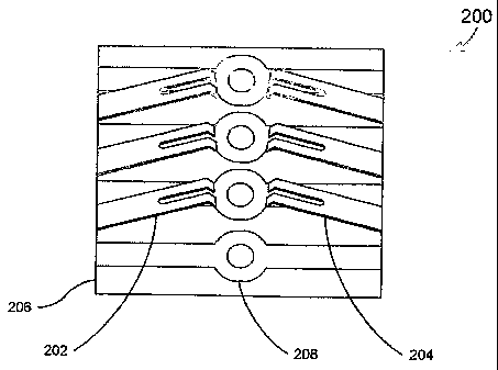
[0035] As is shown in Figs. 2 and 5, a particular implementation of multiple
flat brush
contacts 200 is a pair of such brushes 202 and 204 mounted opposing each other
on a PCB
206 and fed through a central eyelet or via 208. Aside from the advantages of
multiple
brushes for increased current capacity and reduced dynamic resistance, this
implementation also has high-frequency performance benefits. The central
eyelet 208
assures equal length transmission lines and in-phase signals to both brushes
202 and 204,
as well as surge impedances favorable to impedance matching of slip rings and
low loss.
The location of the opposing contact brush tips in close proximity helps to
reduce phasing
errors from the slip ring. With reference to Figs. 1 and 6, the central via
208 also allows
for visual alignment verification of the contact brushes 202 and 204 to a
ring, e.g., ring
106A, which is a highly desirable feature that simplifies slip ring assembly.
[0036] As is depicted in Figs. 7A-7B, at high data rates and high frequencies,
center-fed
brush structures 702 and 704 can be optimally used in differential
transmission lines. The
transmission line geometry shown is typically implemented with a multi-layer
PCB 700.
The flat brush contacts 702 and 704 are surface-mounted to a microstrip
structure 705 over
a ground plane 710. The connection between the brushes 702 and 704 and the
external
-5-
CA 02515831 2005-08-11
WO 2004/075421 PCT/US2004/004613
input terminals takes the form of an embedded microstrip 712. The size and
spacing of the
brush microstrips 705 and the embedded microstrip transmission line 712 that
feeds them
is dictated by the necessity to match the impedance of the external
transmission line and
associated slip ring. The via holes for connection of external transmission
lines and
associated central feed via 708 completely penetrate the PCB 700 and have
relief areas
714 in the ground plane 710 for electrical isolation. Two PCBs can be bonded
back-to-
back to feed two slip rings, with the vias penetrating both boards in an
analogous fashion.
[0037] As is illustrated in Fig. 8, multiple brush structures can be
implemented utilizing
PCB techniques, as described above, to create transmission line sections of
the correct
impedance. For example, assuming the use of 50 Ohm cabling, the "crossfeed"
transmission lines 802 and 804 are designed for a differential impedance of 50
Ohms,
matching the external feedline. The parallel connections to the brush
structures are by
means of equal length transmission lines 806 and 810. Such transmission lines
that
provide in-phase signals to the brush structures are referred to in this
document as "zero-
degree phasing lines," in keeping with a similar expression used for phased
antenna arrays.
The impedance of these "zero-degree phasing lines" is twice that of the
"crossfeed lines,"
or 100 Ohms. The differential impedance of the slip ring utilized with a
contact structure
800, as illustrated in Fig. 8, is then two times that of the phasing lines 806
and 810, or 200
Ohms. A general solution to parallel feed of N contact structures establishes
the
differential impedance of the phasing lines as N times the input impedance.
[003] In those instances in which the impedances are not convenient or
achievable
values, the use of a gradated (i.e., changing in a continuous, albeit almost
imperceptible,
fashion) impedance transmission line 900 can be used as a matching section
between
dissimilar impedances. With reference to Fig. 9, a diagram illustrates a
gradated
impedance matching section, which shows a tapered parallel differential
transmission line
900. Tapering the traces 902 and 904 is one method of continuously varying the
impedance, which minimizes the magnitude of the reflections that would
otherwise result
from abrupt impedance discontinuities.
[0039] Fig. 10 illustrates the use of gradated impedance transmission lines as
a solution
for ameliorating the effects of dissimilar impedance values. In this example,
the
differential impedance of the slip ring associated with the contact system is
too low to
conveniently match the phasing lines, as described in conjunction with Fig. 8.
The taper
of the crossfeed lines 1002 and 1004 allows the impedance of the transmission
line to be
-6-
CA 02515831 2005-08-11
WO 2004/075421 PCT/US2004/004613
gradually reduced to an intermediate value of impedance between that of the
rings of the
slip ring platter and the external transmission line. The taper of the zero-
degree phasing
lines 1006 and 1010 allows the impedance to be gradually increased from that
of the slip
ring to match the intermediate value described above. The net effect of
utilizing gradated
impedance matching sections is to reduce the magnitude of the reflections from
what
would otherwise be substantial impedance mismatches. The minimizing of
impedance
discontinuities is desirable from the standpoint of preserving signal
integrity of high-speed
data waveforms.
[00401 Another technique for constructing a contact system for slip rings
functioning
beyond one GHz is shown in Fig. 11. This technique utilizes a microstrip
contact 1100 to
preserve the transmission line characteristics to within a few millimeters of
the slip ring
before transitioning to the contacts 1102 and 1104. The microstrip contact
1100 acts as a
cantilever spring to provide correct brush force, as well as providing an
impedance
controlled transmission line. Thus, the microstrip contact 1100 acts
simultaneously as a
transmission line, a spring and a brush contact, with performance advantages
beyond one
GHz. The embodiment of Fig. 12, which depicts the contact 1100 of Fig. 11 in
conjunction with a slip ring platter 1120, functions to provide a single high-
speed
differential data channel of a broadband slip ring.
Flat-Form PCB Broadband Slip Ring Platter
[00411 Systems that implement a broadband slip ring platter with a flat
interdigitated
brush contact system are typically implemented utilizing multi-layer PCB
techniques,
although other techniques are also possible. High-frequency performance is
enhanced by
the use of low dielectric constant substrates and controlled impedance
transmission lines
utilizing microstrip, stripline, coplanar waveguide and similar techniques.
Further, the use
of balanced differential transmission lines is an important tool from the
standpoint of
controlling electromagnetic emission and susceptibility, as well as common-
mode
interference. Microstrip, stripline and other microwave construction
techniques also
promote accurate impedance control of the transmission line structures, a
factor vital to the
wide bandwidths necessary for high-frequency and digital signaling. A specific
implementation depends primarily upon the desired impedance and bandwidth
requirements.
-7-
CA 02515831 2005-08-11
WO 2004/075421 PCT/US2004/004613
[0042] Figs. 13A-13B show an electrical diagram and a partial cross-section,
respectively,
of a slip ring platter 1300 utilizing microstrip construction, with conductive
rings 1302A
and 1302B etched on one side of a PCB dielectric material 1304, with a ground
plane 1310
on the opposite side. The PCB material 1304 is chosen for the desired
dielectric constant
that is appropriate for the desired impedance of the slip ring platter 1300.
Connections
between the conductive rings 1302A and 1302B and the external transmission
lines are
accomplished by embedded microstrips 1306A and 1306B, respectively.
Microstrips
1306A and 1306B are typically routed to a via or surface pad for attachment to
wiring or
other transmission line. Connections between the feedlines 1306A and 1306B and
the
rings 1302A and 1302B are provided by vias that run between the two layers.
The
structure shown is typically a three-layer structure, or five to six layers if
constructed as a
double-sided slip ring platter. The ground plane 1310 can be a solid or a mesh
construction depending upon whether the ground plane is to act as an
additional
impedance variable and/or to control board distortion.
[0043] Negative barrier 1320, i.e., a groove machined between the rings,
accomplishes
some of the functions of a more traditional barrier, such as increasing the
surface creep
distance for dielectric isolation and to providing physical protection against
larger pieces
of conductive debris. The negative barrier 1320 used in a high-frequency slip
ring platter
also has the feature of decreasing the effective dielectric constant of the
ring system by
replacing solid dielectric with air. The electrical advantage of this feature
is that it allows
higher impedance slip ring platters to be constructed than would otherwise be
practical for
a given dielectric.
[0044] The rings 1302A and 1302B can be fed either single-ended and referenced
to the
ground plane 1310 or differentially between adjacent rings. As is described
above, the
feedlines 1306A and 1306B can be either constant width traces sized
appropriately for the
desired impedance or can be gradated impedance transmission lines to aid in
matching
dissimilar impedances.
[0045] The PCB slip ring construction, described above, provides good high-
frequency
performance to frequencies of several hundred MHz, depending upon the physical
size of
the slip ring platter and the chosen materials. The largest constraint to the
upper frequency
limit of such a slip ring platter is imposed by resonance effects as the
transmission lines
become a significant fraction of the wavelength of the desired signal.
Typically,
reasonable performance can be expected up to a ring circumference of about one-
tenth the
-8-
CA 02515831 2005-08-11
WO 2004/075421 PCT/US2004/004613
electrical wavelength of the signal with reasonable values of insertion loss
and standing
wave ratio.
[0046] To accommodate higher frequencies or bandwidths for a given size of
slip ring, the
resonant frequency of the slip ring must generally be increased. One method of
accomplishing this is to divide the feedline into multiple phasing lines and
drive the slip
ring at multiple points. The effect is to place the distributed inductances of
the slip rings
in parallel, which increases the resonant frequency proportional to the square-
root of the
inductance change. Fig. 14 shows a feed system 1400 that uses differential
transmission
lines and Fig. 15 shows a cross-section of a PCB slip ring platter that
incorporates the feed
method. Two phasing lines and associated feedpoints are shown in the example,
although
three or more phasing lines can be used with appropriate allowance to matching
the
impedances.
[0047] The transmission line to rings 1402 and 1404 are connected to points
1401 and
1403, respectively, in both Figs. 14 and 15. The crossfeed transmission lines
1406 and
1408 are designed to match the impedance of the feedline, 50 Ohms in this
example. The
parallel combination of phasing lines 1410A and 1410B and 1412A and 1412B are
also
designed to match the 50 Ohm impedance, or 100 Ohms individually. Each phasing
line
connection sees a parallel section of the rings 1402 and 1404, which, in this
example, are
designed for a 200 Ohm differential impedance. Other combinations are possible
as well
with appropriate adjustments to match impedances. Specifically, where N is the
number
of slip ring feedpoints and Z is the input impedance, the phasing line
impedance is N*Z
and the ring impedance is 2*N Z. Achieving higher impedance values is
facilitated by the
use of low dielectric constant materials. The phasing lines shown in Fig. 15
benefit from
the proximity of the air in the negative barrier to achieve a lower dielectric
coefficient and
higher differential impedance.
[0048] The use of flexible circuitry 104 (see Fig. 1) in the construction of
gradated
impedance phasing line sections facilitates multi-point connections to rings
106A and
106B of PCB slip ring platter 102. This method simplifies the construction of
the PCB
slip ring as the phasing lines are external to the ring and are readily
connected in parallel at
the crossfeed transmission line. The gradated impedance matching sections
allow the
construction of slip rings with smooth impedance profiles, which improves
passband
flatness and signal distortion due to impedance discontinuities. The use of
gradated
-9-
CA 02515831 2005-08-11
WO 2004/075421 PCT/US2004/004613
impedance phasing lines is generally a desirable feature when constructing
broadband
PCB slip rings 100.
Slip Ring Mounting Method
[0049] Figs. 16 and 17 depict a rotary shaft 1600, for receiving a plurality
of slip ring
platter assemblies 100, that is advantageously designed to facilitate
construction of a slip
ring, while addressing three typical concerns encountered in the manufacturing
of these
devices. As designed, the shaft allows for control of axial positioning of the
platters
without tolerance stack-up, control of radial positioning of the platter slip
rings and wire
and lead management. A significant difficulty when mounting slip ring platters
to a rotary
shaft is avoiding tolerance stack-up that is inherent with many slip ring
mounting methods,
e.g., those using spacers. Wire and lead management is also a perennial
problem with the
manufacture of most slip rings as wire congestion increases with each
additional platter.
As is best shown in Fig. 16, the rotary shaft 1600 includes a number of steps
that address
the above-referenced issues.
[0050] The shaft 1600 may be a computerized numerical control (CFTC)
manufactured
component with a series of concentric grooves machined to produce a helical
arrangement
of mounting lands/pads 1602-1612 for the platters 102 of the slip ring system.
The axial
positioning of the grooves on the shaft 1600 are a function of the
repeatability of the
machining operation, thus one side of each slip ring is located axially to
within machining
accuracy with no progressive tolerance stack-up. The opposite side of each
platter 102 is
positioned with only the ring thickness tolerance as an additional factor. The
inside
diameter of the grooves is sized to provide a radial positioning surface for
the inside
diameter of each platter. The helically arranged lands/pads 1602-1612 provide
mounting
features for each platter 102. The helical arrangement provides more wire way
space as
each platter 102 is installed. The shape of wire way 1640 provides a way for
grouping
wiring 1650 for cable management and electrical isolation purposes. As is
shown in Fig.
17, the shaft 1600 may be advantageously located within a cavity 1660 of a
form 1670
during the construction of the multiple platter slip ring system.
[0051] In summary, a slip ring system incorporating the features disclosed
herein provides
a high-frequency broadband slip ring that can be characterized by the
following points,
although not necessarily simultaneously in a given implementation: the use of
flat
interdigitated contacts in conjunction with flat PCB slip rings and
transmission line
-10-
CA 02515831 2005-08-11
WO 2004/075421 PCT/US2004/004613
techniques to achieve wide bandwidths; use of brush contact structures that
include a
central via coupled to a feedline, which provides performance advantages and
allows for
visual alignment verification between rings and brushes; PCB construction of
differential
transmission lines for multi-point feeding of slip rings; the use of multiple
flex tape
phasing lines for multi-point feeding of slip rings; the use of gradated
impedance
transmission line matching sections to affect impedance matching in PCB slip
rings in
general and specifically in the above applications; the use of a negative
barrier in PCB slip
ring platter design for its electrical isolation benefits as well as its high-
frequency benefits
attributable to a lower dielectric constant; the use of microstrip contacts,
i.e., a flexible
section of microstrip transmission line with embedded contacts to provide high-
frequency
performance advantages over more traditional approaches; and the use of a
rotary shaft
with steps in slip ring construction for technical improvements in mechanical
positioning
and wire management.
[0052] The above description is considered that of the preferred embodiments
only.
Modifications of the invention will occur to those skilled in the art and to
those who make
or use the invention. Therefore, it is understood that the embodiments shown
in the
drawings and described above are merely for illustrative purposes and not
intended to limit
the scope of the invention, which is defined by the following claims as
interpreted
according to the principles of patent law, including the doctrine of
equivalents.
-11-