Note: Descriptions are shown in the official language in which they were submitted.
CA 02515956 2005-08-12
WO 2004/073040 PCT/US2004/004211
DESTRUCTIVE ELECTRICAL TRANSIENT PROTECTION
The present invention generally relates to destructive transient suppression
in
semiconductor devices and circuits, and moxe particularly to electrostatic
discharge
protection for semiconductor devices and integrated circuits.
Semiconductor devices and integrated circuits are prone to damage from high
voltage
transients. 'These transients may arise from electrostatic discharge (ESD) or
from other
causes, as for example, an electromagnetic pulse (EMP) caused by a nuclear
explosion,
lightning or other terrestrial, atmospheric or space electromagnetic event. As
used
herein, and not intended to be limiting, the term electrostatic discharge and
the
abbreviation ESD are intended to include all of the above and any other form
of
potentially destructive electrical transient to which a device or circuit may
be exposed,
irrespective of the physical origin of the transient. Also, for convenience of
explanation
1 S and not intended to be limiting, as used herein the term integrated
circuit and the
abbreviation "IC" are intended to include individual semiconductor devices,
interconnected arrays of semiconductor devices on a monolithic or other
substrate,
discrete devices and monolithic interconnected device arrays on a circuit
module or
circuit board or flexible circuit tape, and combinations thereof.
ESD is a very common phenomenon that often arises when ICs are stored,
shipped, handled and used. For example, without being aware of it, a person
about to
handle ox use an IC may become electrostatically charged. When such person
touches
the IC, this stored electrostatic energy may suddenly discharge through the
device or
circuit. Unless provision is made to absorb this ESD energy and limit the
voltage
appearing at the external or internal nodes of the IC, damage may result. It
is not
unconnmon to encounter ESD voltages of 103-104 volts whereas many ICs can be
damaged by voltages of 102 volts or less. Low voltage ICs with normal
operating
voltages of only a few volts are especially vulnerable.
It has been commonplace for many years to include ESD protection devices or
circuits in ICs, especially ICs that employ fteld effect transistors (FETs),
such as for
example, MOSFET and JFET devices. MOSFET devices are further subdivided into
IVMOS and PMOS types and further sub-types and combinations such as CMOS.
These
CA 02515956 2005-08-12
WO 2004/073040 PCT/US2004/004211
2
terms and abbreviations are well known in the art. ESD protection devices are
usually
provided at the input/output (I/O) connection pads of the IC since these nodes
are most
likely to receive an ESD pulse, but they can also be provided anywhere within
or
external to the IC. As used herein, the terms "pad", "I/O pad" and "I/O node"
are
indented to include any node within or on an IC desired to be protected from
ESD. The
ESD protection device is typically coupled between the I/O node and ground or
other
reference voltage line or substrate. As used herein, the term "ground" is
intended to
include any line, rail, bus, substrate or other connection used as a reference
level for the
IC irrespective of its actual voltage level.
During normal circuit operation, the ESD device is inactive and does not
interfere with normal circuit operation. But when the I/O node receives an ESD
pulse,
the ESD protection device turns on to limit the voltage that appears at the
protected
node and associated devices internal to the IC that are coupled to this node,
and to
harmlessly dissipate the energy of the ESD pulse. As soon as the ESD pulse has
passed,
the ESD protection device once again becomes inactive. Thus, the ESD device
functions as a transient voltage clipper that limits the ESD voltage appearing
on the I/O
pads or other nodes of the IC to a safe level and that provides a harmless
current path to
ground or the like.
As IC technology has advanced and individual devices within the IC made
faster and smaller, the ESD protection problem has been exacerbated. For
example, the
use of silicided contacts, very short channel lengths and decreasing
source/drain gate
contact spacings, has drastically reduced the ability of NMOS output devices
to
inherently provide ESD protection. Various solutions have been proposed in the
prior
art, for example: (1) Duvvury and Diaz in a paper entitled "Dynamic Gate
Coupling of
NMOS for° E~cient Output ESD Protection" published in the Proceedings
of the IRPS
in 1992, pp 141-150, describe the use of gate coupling to improve ESD
protection in
silicided and LDD technology devices; (2) Verhaege and Russ in a paper
entitled
"Wafer- Cost Reduction through Design of High Performarace Fully Silicided ESD
Devices" published in the EOS/ESD Symposium Proceedings in 2000, pp 18-28,
describe a mufti-finger turn-on technique coupled with the use of back-end
ballast
segmentation for improving ESD protection, and (3) Mergens et al in a paper
entitled
"Mufti-Finger Tisrrr-on Circuits and Design Techniques for- Enharaced ESD
CA 02515956 2005-08-12
WO 2004/073040 PCT/US2004/004211
Perfo~nzance witla Widtlz Scaling" published in the EOS/ESD Symposium
Proceedings
in 2001, pp 1-11, describe both domino and mufti-forger turn-on devices with
merged
ballasts.
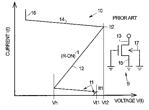
In many of these approaches, output NMOS device 9 shown in FIG. 1 operates
as parasitic bipolar NPN device with N-type drain 13 as collector, P-type body
17 as
the base and N-type source 15 as the emitter. The body can be, for example,
the
substrate in a CMOS bulk process, the P-well of an epi process or a P-well
isolated by
an N-type tub as in a BiCmos process. FIG. 1 also shows current-voltage
characteristic
of a device of this type. As the voltage V(t) across the source- source-drain
terminals
10 of the device increases it is triggered into conduction at voltage Vtl and
current Itl . Vtl
is the collector-base breakdown voltage of the parasitic NPN with the base
connected to
the emitter through the p-type base body resistance. The current increases and
the
voltage drops to holding voltage Vh along path 11.
During the ESD event the device operates mostly in "snapback" region 11, 12.
At higher stress levels, the device approaches second breakdown at voltage Vt2
and
current It2. The voltage across the device then drops again and the current
rises very
rapidly along lines 14, 16, indicating that some form of catastrophic failure
has
occurred. With very low current devices, by the time the voltage has reached
Vt2, some
damage to the device may already have occurred resulting in increased leakage
even if
normal operation resumes.
The slope of snapback region 12 is the dynamic conductance, that is (R-ON)-1.
Generally, according to the prior art, to provide ESD protection while
avoiding
damage, the condition Vt2 > Vtl must be satisfied. It is common in the prior
art to use
multiple parallel devices, e.g., mufti gate-finger NMOS output devices, that
must all
turn on in order to provide ESD protection and to employ ballast resistors for
this
purpose.
While these prior art approaches have been useful, they still suffer from a
number of disadvantages well known in the art, as for example but not limited
to some
or all of: (i) use of breakdown induced ESD turn-on, (ii) larger than desired
device
and/or ballast resistor area, (iii) susceptibility to process fluctuations,
(iv) poor turn-on
efficiency, (v) higher than desired Vtl and Vt2, and (vi) use of potentially
destructive
snap-back device functions and the like to trigger ESD protection. These
disadvantages
CA 02515956 2005-08-12
WO 2004/073040 PCT/US2004/004211
4
are particular troublesome with very low current devices where the increase in
leakage
currents that can result from dissipation of an ESD transient using prior art
devices can
cause circuit malfunction or loss of sensitivity when normal device operation
resumes
after the ESD transient has passed.
Accordingly, it is an object of the invention to provide improved ESD means
and methods for ICs, especially for ESD protection that allows Vh, Vtl and Vt2
to be
approximately equal.
This object is achieved by the circuit of claim 1 and the method of claim S.
Advantageous embodiments of the invention are characterized in the sub-claims.
The circuit of the invention has low ESD device propagation delay, uses little
chip area,
avoids the use of extra processing steps for silicide or LD blocks at the
device, and that
can handle very rapid rise time ESD pulses.
A circuit is provided for protecting ICs against ESD transients. The apparatus
comprises: a master circuit responsive to ESD voltage V(t) and having an
output; and a
slave circuit comprising multiple parallel shunt devices having a common input
coupled to the output of the master circuit; wherein as V(t) increases the
master circuit
applies a portion of V(t) to the input of the slave circuit shunt devices
thereby lowering
a threshold voltage Vtl at which the slave circuit shunt devices would
otherwise turn
on, to a smaller value Vtl' much closer to a holding voltage Vh of the shunt
devices;
~ and wherein when V(t) reaches Vtl', all of the slave circuit devices turn on
substantially simultaneously, thereby shunting the ESD transient harmlessly to
ground.
The master circuit and slave circuits are desirably inactive during normal
device
operation.
A method is provided for harmlessly shunting a transient voltage V(t)
appearing
on a node of an IC to ground. The method comprises: dividing the transient
voltage
V(t) to obtain a reduced transient voltage Vmi; coupling the reduced voltage
Vmi to a
control terminal of an active device whose output terminal is coupled to a
reference
ground of the IC through a resistance, to produce an output voltage;
substantially
simultaneously coupling the output voltage to inputs of multiple parallel
active devices
whose power terminals are coupled between the node and the reference ground,
wherein the output voltage reduces turn-on voltages of the multiple parallel
active
devices to a level sufficient to cause the multiple parallel devices to turn
on
CA 02515956 2005-08-12
WO 2004/073040 PCT/US2004/004211
substantially simultaneously, thereby clamping the transient voltage appearing
at the
node to a safe level.
Embodiments of the present invention will hereinafter be described in
conjunction with
the following drawing figures, wherein like numerals denote like elements, and
5 FIG. 1 shows the typical current voltage characteristics of a prior art
parasitic
NPN snapback type ESD protection device;
FIG. 2 is a simplified schematic diagram illustrating an ESD protection
arrangement of the present invention according to a first embodiment;
FIG. 3 shows current voltage characteristics of an ESD protection arrangement
of the present invention, compared to the characteristic of FIG. l;
FIG. 4 is a simplified schematic diagram illustrating an ESD protection
arrangement of the present invention according to a further embodiment; and
FIG. 5 is a simplified schematic diagram illustrating an ESD suppression
arrangement according to a still further embodiment of the present invention.
FIG. 2 is a simplified schematic diagram illustrating ESD protection circuit
20
according to the present invention. Protection circuit 20 is coupled to
bonding pad or
other IC node 22, and to other portions of the IC as indicated by arrow 24.
Circuit 20
comprises master circuit 26 coupled to slave circuit 28.
Master circuit 26 comprises NMOS transistor Nm, Resistor Rl, resistor R2,
resistor R3 and capacitor Cl. Resistor Rl is coupled between pad 22 and node
33,
which is coupled to drain contact 42 of transistor Nm and to lead 37 of
capacitor 38.
Resistor R2 is coupled between node 46 and ground or other reference level 50.
Node
46 is in turn is coupled to lead 39 of capacitor 38 and gate 48 of transistor
Nm. Resistor
R3 is coupled between~source terminal 44 of transistor Nm at node 31 and
ground 50.
Node 31 is coupled to the control terminals G1, G2, .... Gn of transistors
Nsl, Ns2,
Nsn of slave circuit 28.
The master circuit comprises a transient voltage divider having a first
resistor
Rl , a capacitor C1 and a second resistor R2 series coupled between V(t) and
ground,
and an active device having a control terminal Tl and power terminals T2, T3,
wherein
T1 is coupled to a first terminal of C1 whose second terminal is coupled
through R2 to
V(t), Tl is also coupled to a first terminal of R2 whose second terminal is
coupled to
ground, T2 is coupled to a second terminal of C1 and through R2 to V(t), and
T3 is
CA 02515956 2005-08-12
WO 2004/073040 PCT/US2004/004211
coupled through a third resistor R3 to ground, wherein the output of the
master circuit
is derived from T3. The master circuit comprises a transient voltage divider
having a
time constant at least 5 times the ESD transient rise time to Vtl'. Rl, R2 and
C1 are
chosen so that during the time wherein the ESD transient rises to about Vtl',
there is
negligible voltage drop across C1.
Power terminals Dl, D2 .... Dn (e.g., drains) and S1, S2 ... Sn (e.g.,
sources) of
slave transistors Nsl, Ns2, ... Nsn are coupled between line or rail 40
running to pad 22
and ground 50. Slave circuit 28 desirably comprises an n-fingered NMOS clamp
device, with the multiple fingers creating parallel devices Nsl, Ns2, ... Nsn.
The ESD
voltage appears on line 40 and needs to be harmlessly discharged to ground 50
without
permitting damage to any devices or other portions of the IC coupled (as
indicated by
arrow 24) to pad 22.
The multiple parallel shunt devices comprise NMOS transistors having gates
coupled to the slave circuit input, collectors coupled to V(t) and sources
coupled to a
ground potential, and further comprising parasitic NPN bipolar transistors
formed by
the NMOS drains acting as collectors and a P substrate or well regions of the
NMOS
transistor acting as bases and the NMOS sources acting as emitters, whereby
Vtl and
Vtl' are the collector-base breakdown voltages of the parasitic NPN
transistors
respectively without and with bias applied to the NMOS gates, wherein Vtl' <
Vtl.
When an ESD event occurs and the ESD voltage begins to appear on line or bus
40,
master circuit 26 reacts quickly and turns on all parts of slave circuit 28 at
substantially
the same time, thereby clamping the voltage on line 40 and pad 22 to a safe
level
determined by holding voltage Vh of slave circuit devices Nsl ... Nsn, and any
series
resistance in the shunt path provided by slave circuit 28. This protects the
remainder of
the IC coupled to pad or node 22 via connection 24. It should be noted that
device Nm
is operating in a normal manner, that it, it is not required to go into any
form of
breakdown in order for slave circuit 28 to clamp and shunt the ESD pulse.
Among
other things, this provides very fast protection turn-on and makes the present
invention
much less susceptible to process fluctuations that can otherwise affect the
breakdown
characteristics of prior art ESD protection devices used without master
circuit 26.
Resistors Rl, R2 and capacitor C1 form an RC circuit across which appears the
transient ESD pulse voltage Vp. It is desirable that resistors Rl, R2 have
relatively
CA 02515956 2005-08-12
WO 2004/073040 PCT/US2004/004211
7
large values so that capacitor C1 can be made small and still provide an RC
time
constant that is in the appropriate range. Rl, R2 are preferably about equal,
as for
example about 100,000 Ohms each, but larger or smaller values can also be
used.
Resistor R3 is preferable about 40 % of Rl, R2, for example, about 40,000
Ohms, but
larger or smaller values can be also used. Methods for producing compact high
value
resistors for ICs are well known in the art. Capacitor C 1 is desirably chosen
so that time
constant circuit of the master circuit is at least an order of magnitude
larger than the
time required for the slave device to enter full snapback. The time constant
should be a
balance between a) the rise time of digital inputs, b) the time for the slave
device to
enter full snapback, and c) the desired trigger voltage and could vary widely
depending
on technology and application. A value for C1 of about 0.1 picofarads is
suitable but
larger or smaller values can also be used.
Consider the situation when an ESD transient V(t) is applied to pad 22 and
line
40 wherein the ESD pulse rises from V(t) = 0 to about 7 volts in the first 0.1
nanoseconds. This is equivalent to a rise time about 7 x 101° volts per
second, an
extremely rapid rise time. Nonetheless, pulses with rise times of this
magnitude can be
encountered during ESD events.
Resistors Rland R2 series coupled via capacitor C1 act as a transient voltage
divider. Voltage Vgm appearing at gate 48, and voltage Vmi appearing on node
46 are
the same. The transient voltage drop Vc(t) across C 1 is about zero during the
ESD
pulse rise time because of the large dv/dt, so voltage Vdm appearing at drain
42 of
master transistor Nm is about equal to Vmi and Vgm. Rl and R2 are conveniently
about equal, so that Vmi at node 46 is about half the magnitude of voltage Vp
on line
40. Thus, when voltage V(t) on pad 22 and line 40 reaches about V(t) = Vp = ~7
volts
Vrni = Vgm = Vdm are about 3.5 volts.
Master transistor Nm acts as a source follower so that voltage Vsm appearing
at
source 44 of master transistor Nm 30 and voltage Vsi at the input to slave
circuit 28 are
equal to Vgm - Vth, where Vth is the threshold voltage of transistor Nm, in
this
example about 0.5 volts. Thus, a voltage equal to about Vsi = Vp/2-Vth(Nm)
(e.g., 7/2 -
0.5 = ~ 3 volts) appears at node 31 and on all of the gates or gate ringers of
slave
transistors Nsl, Ns2, ... Nsn. The time delay is determined substantially by
the
switching time of Nm which is very fast, of the order of RC/10 to RC/100
seconds from
CA 02515956 2005-08-12
WO 2004/073040 PCT/US2004/004211
8
when the ESD transient V(t) reaches the predetermined voltage V(t) = Vp. Thus,
voltage Vsi = Vp/2-Vth(Nm) is applied substantially simultaneously to all of
the gates
Gl, G2, ... Gm of transistors Nsl, Ns2 ... Nsn (collectively slave transistors
28) a very
short time after the ESD pulse reaches the predetermined voltage Vp, about 7
volts in
this example.
It is known that Vtl is reduced by applying a voltage to gates Gl, G2, ... Gn
of
clamp devices Nsl, Ns2, ... Nsn. This is used in the prior art by coupling the
gates G1,
G2, ... Gn of the clamp~devices Nsl ... Nsn to body 17 (FIG. 1) or to
resistors placed in
the source-ground lead of devices Nsl, Ns2, ... Nsn (e.g., see slave circuit
28' in FIG.
4). With this prior art arrangement, that is, without master circuit 26, one
of the rnulti-
fingered devices (e.g., Nsl) must first trigger into snap-back at unmodified
threshold
Vtl before there is a bias voltage available on the gates G2 ... Gn of the
remaining
devices Ns2, ... Nsn. Once a first clamp device has triggered at Vtl, then a
voltage is
available on the gates G2 ... Gn. This lowers the threshold voltage Vtl of the
remaining
clamp devices Ns2, ... Nsn to a value below the ESD voltage V(t) so that
remaining
clamp devices Ns2 .... Nsn all turn on together. A disadvantage of this prior
art
arrangement is that the snap-back transition of the first device does not
occur until V(t)
reaches unmodified threshold voltage Vtl, thus exposing the IC to a higher
V(t). A
further disadvantage is that the snap-back transition is relatively slow, thus
the turn on
of the remaining clamp devices Ns2 .... Nsn is delayed by the turn-on time of
the first
clamp finger to fire (e.g., Nsl). With a very rapidly rising transient V(t)
this can
increase the stress to which the IC is exposed since the turn-on of the first
finger may
not provide sufficient clamping action to clip the rising V(t) transient.
The circuit of the present invention operates differently. All of the gates of
the
slave devices N1, N2, ... Ns are driven by the output of master circuit 26.
Thus, as soon
as the voltage on node 46 rises above Vth(Nm), Nm begins to conduct, thereby
raising
Vsi applied to gates G1, G2, ... Gn. Unlike the prior art, this occurs before
V(t) reaches
Vtl . Thus, with the present invention, all of clamp devices Nsl, Ns2, ... Nsn
turn on at
the same time and at significantly lower values of V(t), e.g., at V(t) = Vtl'
« Vtl.
Vt1 decreases as Vsi increases. Vtl usually has a minimum Vtl(min) as a
function of
Vsi, often very near Vh. While the above noted values for Rl, R2, R3 and C 1
are
convenient, larger and smaller values can be used depending on the value of
V(t) = Vp
CA 02515956 2005-08-12
WO 2004/073040 PCT/US2004/004211
9
at which clamping action is desired to be initiated. Rl, R2, R3 be chosen so
that when
the ESD transient voltage V(t) applied to pad 22 and rail 40 reaches
predetermined
value V(t) = Vp, that Vsi = Vp/2-Vth(Nm) is sufficiently large to reduce Vtl
to about
Vtl' = Vtl(min), where Vtl(min) is the minimum value of Vtl as a function of
gate
voltage applied to clamp devices Nsl, Ns2, ... Nsn, or stated alternatively to
reduce
Vtl' to be about Vtl' ~ Vh. The value of Vsi to accomplish this will vary with
the
technology used to construct devices Nsl, Ns2, ... Ns but those of skill in
the art will
know how to determine the desired Vsi without undue experimentation.
FIG. 3 shows the current voltage properties 60 of circuit 20 of the present
invention in response to such an ESD transient, in comparison to the
characteristic
shown in FIG. 1. The current - voltage characteristic of FIG. 1 is shown on
FIG. 3 by
dashed lines. Applying.the voltage Vsi to gates Gl, G2, ... Gn of slave
transistors 28 of
the present invention has the effect of lowering the value Vtl of the
collector-base
breakdown of the parasitic bipolar NPN transistors formed by drains D1, D2,
... Dn as
the collectors, sources S1, S2, ... Sn as the emitters and substrates Sbl,
Sb2, ... Sbn as
the base. Thus, with Vsi applied to gates G1, G2, ... Gn, Vtl drops to Vtl'
and slave
circuit 28 turns on along path 61. This occurs for all of slave transistors 28
substantially
simultaneously, that is, they all turn on together. Thus, the clamp function
provided by
the multiple fingers of slave transistors 28 occurs substantially all at the
same time. As
noted above, this is in contrast to many prior art arrangements where at least
one clamp
transistor finger must reach collector breakdown threshold Vtl before any Vtl
lowering
action propagates to the other fingers.
As can be seen in FIG. 3, this modified value Vtl' obtained in the present
invention is close to Vh, that is, off set 67 between Vtl' and Vh is generally
within
about 20 % of Vh, preferably as close as possible to Vh so that the clamping
action is
very efficient and very quick. As the ESD transient continues the slave
circuit current
rises along line 62 of FIG. 3. It will be noted that the dynamic conductance
[(R-on)-I]'
of the present invention is much steeper than (R-on)-1 of the prior art
arrangement
illustrated by line 12 in FIG. 1 and FIG. 3. Thus, the clamping action of the
present
invention is very robust. It will also be noted that Vt2' is much lower than
Vt2 of the
unbiased transistors Nsl, Ns2, ... Nsn and that Vtl', Vt2' and Vh are of
similar
magnitude. More specifically, offset 69 between Vt2' and Vtl' is generally
within 20
CA 02515956 2005-08-12
WO 2004/073040 PCT/US2004/004211
of Vtl', more conveniently within about 10 % of Vtl' and preferable within
about 5
of Vtl', although larger and smaller values are useful. Vt2' can be made
closer to Vh
by increasing the number of fingers in the clamp devices Nsl, Ns2, ... Nsn.
Vtl' is a
function of gate voltage, and process technology.
The steepness of region 62 can be adjusted by increasing or decreasing the
number of fingers, that is, the number of parallel transistors in slave
circuit 28.
However, for the same number of fingers and active clamp device area, region
62 of the
present invention will be steeper than region 12 of the prior art during the
initial turn-on
of the ESD clamp because all fingers become conductive at the same time. It is
10 desirable to include a sufficient number of parallel fingers (transistors
Nsl...Nsn) so
that the anticipated worst case ESD charge can be dissipated while remaining
in safe
operating area (SOA) 65 extending from Itl' to It2" where It2" is less than
It2'. It is
desirable to derate the design maximum current density, It2" by 25% from the
measured value of It2' to ensure an adequate guard band. However, in cases
where
extremely low post-pulse leakage is required, It2" must be de-rated by as much
as 75 to
90% from It2'. This is to minimize the risk of partial damage to the IC as
I(t)
approaches It2' that might result in increased IC leakage once the ESD
transient has
passed.
The simultaneous finger turn-on provided by the present invention is superior
to
prior art approaches where the clamp device or finger turn-on is sequential
(cascaded),
that is, where one finger turns on and current flow through this first
triggers another
finger which in turn causes yet another finger to turn on and so forth. Each
subsequent
turn-on increases the current carrying capacity of the prior art clamp
circuit. In other
prior art, the first finger turns on, triggered at avalanche-dependent Vtl,
which then
fires all the other fingers simultaneously. However if the rise time of the
ESD transient
is very fast, the cascaded turn-on may not keep pace and less ESD protection
is
obtained or is undesirably rise-time sensitive. With the present invention,
the high
speed master circuit and the substantially simultaneous turn-on of the slave
circuit
transistors avoids this problem of the prior art. Even the so-called
simultaneous turn-on
approaches of the prior art require at least one finger to enter the snap-back
mode at
Vtl in order to turn on other fingers at a reduced voltage less than Vtl . The
present
invention avoids this limitation.
CA 02515956 2005-08-12
WO 2004/073040 PCT/US2004/004211
11
A further advantage of the present invention is that it scales linearly, that
is, the
total current carrying capacity of the clamp circuit is proportional to the
width of slave
transistors 28, e.g., the number of parallel gate fingers. While this property
is also
possessed by some prior art arrangements, it is nonetheless an important
feature that
greatly facilitates design of ESD protection for different applications. An
ESD
protection solution that does not possess this property is less desirable.
A still further advantage of the present invention is that master circuit 26
with
transistor Nm does not enter the snapback regime, that is, there is no risk of
snapback
or second breakdown in master stage 26. Resistor R3 decreases the voltage
appearing
across the source-drain and from the drain to body of transistor Nm preventing
it from
entering the snapback mode. This is an important advantage since having any
transistor
enter the snap-back mode at large values of Vtl increases the risk that some
partial
damage will occur and parasitic leakage will increase after the ESD transient
has
passed. This is especially important in very low voltage ICs designed for low
power
applications where low parasitic leakage is a significant design objective. A
further
advantage of avoiding snapback in the master stage is that snapback is
relative slow
process since the time required to enter full snapback depends on the base
transit time
of the parasitic NPN transistor. Accordingly, master circuit 26 operates much
faster
than if it depended on snap-back for triggering slave devices 28, 28'
FIG. 4 is a simplified schematic diagram illustrating ESD protection
arrangement 80 according to a further embodiment of the present invention.
Substrate
diodes Sbl, Sb2 ... Sbn are not shown in FIG. 4-5 for simplicity and
convenience of
explanation, but persons of skill in the art will understand that they are
present. Circuit
80 of FIG. 4 differs from circuit 20 of FIG. 2 in that series drain
resistances Rdl, Rd2,
... Rdn and series source resistances Rsl, Rs2, ... Rsn are included in slave
circuit 28'.
Convenient values for these resistances are of the order of 10° to 102
Ohms with about
5 ohms being preferred, but larger or smaller values can also be used. These
resistances
are useful in equalizing current flow through multiple transistors Nsl, Ns2,
... Nsn
during the ESD event when in conduction regions 61, 62 of FIG. 3. Diodes Dil,
Di2, ...
Din are desirably coupled between sources S1, S2, ... Sn and gates G1, G2, ...
Gn of
transistors Nsl, Ns2, ... N2n, respectively. In the event that master circuit
26 fails to
operate for some unexpected reason, for example when transistor Nm has a
hidden
CA 02515956 2005-08-12
WO 2004/073040 PCT/US2004/004211
12
manufacturing defect, then diodes Dil, Di2, ... Din will cause transistors
Nsl, Ns2,
Nsn to turn on in the same way as described in the prior art. Thus diodes Dil,
Di2,
Din act to increase the overall robustness of the protection circuit of the
present
invention by providing a fail-safe mode of operation.
FIG. 5 is a simplified schematic diagram illustrating ESD suppression circuit
90
according to a still further embodiment of the present invention. The circuit
of FIG. 5
has slave portion 28' like slave portion 28' of FIG. 4, but slave portion 28
of FIG. 2
could equally well be used. Master portion 26' of FIG. 5 shows a further
embodiment
in which master portion 26 of FIG. 2 is replaced by master portion 26'. In
master
portion 26', Vmo is generated from V(t) = Vp by means of Zener diode Z1 and
resistor
R4 series coupled between rail 40 and ground 50. Node 31' at the junction of
between
Zener Z1 and resistor R4 and is coupled to gates G1, G2, ... Gn of slave
transistors
Nsl', Ns2' ... Nsn'. Slave portion 28, 28' in FIG. 5 functions in the same
manner as
slave portions 28, 28' in FIGS 2, 4 respectively.
As the ESD generated voltage V(t) rises, node 31' remains substantially at
ground until Zener Zl fires at V(t) = Vp. The voltage Vmo appearing on node
31' is
determined by the combination of the Zener voltage of Zl, resistor R4 and
voltage Vp.
The use of a zener rather than a MOSFET in master circuit 26' can shorten the
time
required to produce voltage Vmo. It is desirable to choose Zl and R4 so that
when V(t)
reaches the level Vp at which it should be clamped, Vmo is sufficient to
reduce Vtl of
transistors Nsl, Ns2, ... Nsn to Vtl' in much the same way as described in
connection
with circuits 20, 80 of FIGS. 2, 4. For example, assume that it is desired
that ESD
protection transistors 28, 28' fire when V(t) = Vp = about 7 volts, then Zl
and R4 are
chosen so that Vmo' about equals Vtl'the voltage necessary to reduce Vtl' to
about its
minimum value for the transistors of slave circuit 28, 28'. For the example
where Vp =
7 volts, this is about Vmo' = 2 to 3 volts and. correspondingly, Z1 is chosen
to have a
Zener voltage of about 4 to 5 volts. R4 is chosen to limit the current through
master
circuit 26' to a sustainable level during the ESD pulse. The Zener voltage
needs to be
above the normal working voltage of the IC that appears on pad 22 and rail 40
so that
master circuit 26' remains substantially inactive during normal IC operation.