Note: Descriptions are shown in the official language in which they were submitted.
CA 02516053 2005-08-12
B 14191.3 SL 1
PROCESS FOR COATING A SURFACE
DESCRIPTION
Technical field
The invention relates to the deposition or attachment
of materials onto surfaces.
The invention relates in particular to a process for
coating a surface, especially to a process for very
adhesively depositing a material onto a surface.
The process of the invention has the objective of
producing an adhesive deposit of materials of any type
onto surf aces of any type .
Prior art
Numerous techniques have been described to date
regarding the coating of surfaces in general, and in
particular regarding the attachment of materials onto
electrically conductive or semiconductive surfaces. The
adhesive deposition of polymers onto electrically
conductive or semiconductive surfaces, the adhesive
deposition of metals onto electrically conductive or
semiconductive surfaces, and the adhesive deposition of
ionic insulators onto electrically conductive or
semiconductive surfaces will be considered hereinbelow,
in this order, in order to demonstrate the numerous
advantages of the present invention.
The operation via which a molecule of interest, for
example a molecule having particular properties, is
attached onto a surface such that it retains thereon
CA 02516053 2005-08-12
B 14191.3 SL 2
all or some of its properties is known as
functionalization. The functionalization of a surface
assumes that the molecule of interest to be attached
and a suitable process for attaching the said molecule
onto the surface are available. Since the molecule of
interest is usually an organic or organometallic
molecule, the process generally used consists in
calling upon the very large library of organic
chemistry reactions by attempting to find functional
groups, respectively on the surface and on the molecule
of interest, which are compatible, i.e. which can
readily - and if possible rapidly - react together.
For example, when a surface containing hydroxyl groups
-OH or amine groups -NH is available, it may be
functionalized by giving the molecule of interest
isocyanate, siloxane, acid chloride, etc. groups, for
example. When the molecule of interest does not include
any functional groups that are directly compatible with
those of the surface, this surface may be
prefunctionalized with a bifunctional intermediate
organic molecule, one of the functional groups of which
is compatible with those of the surface, and the other
with those of the molecule that it is desired to
attach. The intermediate molecule is occasionally
referred to as an adhesion primer, as described in
document [ 1 ] .
From this point of view, it is found that the
functionalization of a surface is merely a particular
case of organic chemistry reactions, in which one of
the two reagents is a surface rather than a molecule in
solution. Admittedly, the kinetics associated with
heterogeneous reactions between a solution and a
surface are substantially different from the analogous
CA 02516053 2005-08-12
B 14191.3 SL 3
reaction in a homogeneous phase, but the reaction
mechanisms are identical in principle.
In certain cases, the surface is activated by
pretreating it so as to create thereon functional
groups with higher reactivity, so as to obtain a faster
reaction. These may especially be unstable functional
groups, formed transiently, for instance radicals
formed by vigorous oxidation of the surface, either
chemically or via irradiation. In these techniques,
either the surface or the molecule of interest is
modified such that - once modified - the attachment
between the two species amounts to a reaction known
elsewhere in the library of organic chemistry
reactions.
Unfortunately, these methods require relatively complex
and expensive pretreatments, such as the use of vacuum
installations for the plasma methods such as chemical
vapour deposition (CVD), the technique of plasma-
assisted chemical vapour deposition (PACVD),
irradiation, etc., which, moreover, do not necessarily
preserve the chemical integrity of the precursors.
Furthermore, it is observed that these methods are
genuinely operational only insofar as the surface to be
treated has an electronic structure similar to that of
an insulator: in the language of physicists, it may be
stated that the surface needs to have localized states.
In the language of chemists, it may be stated that the
surface needs to contain functional groups. On metals,
for example, reactive deposition treatments (CVD,
PACVD, plasma, etc.) allow better attachment of the
deposit to the oxide layer or at the very least to a
substantially insulating segregation layer.
CA 02516053 2005-08-12
B 14191.3 SL
However, when the surface is a conductor or an undoped
semiconductor, such localized states do not exist: the
electronic states of the surface are delocalized
states. In other words, the notion of a "functional
group" in the organic chemistry sense has no meaning,
and it is thus impossible to use the library of organic
chemistry reactions to attach an organic molecule of
interest onto a surface.
Two notable exceptions exist: these are the spontaneous
chemical reactions of thiols described especially in
document [2], and of isonitriles described, for
example, in document [3] on metal surfaces, and
especially on gold surfaces.
However, these reactions cannot be exploited in all
situations. Specifically, thiols, for example, give
rise to weak sulphur/metal bonds. These bonds are
broken, for example, when the metal subsequently
undergoes cathodic or anodic polarization, to form
thiolates and sulphonates, respectively, which desorb.
The means that is currently most commonly used for
attaching organic molecules onto electrically
conductive or semiconductive surfaces is to circumvent
the difficulty by equating it to a known problem. It is
a matter of forming on these surfaces, beforehand,
hydroxyl groups -OH, by ensuring the promotion of a
totally or partially hydrated oxide layer on the metal.
On graphite, which has no solid oxide, anodization
nevertheless produces hydroxyl groups, which may be
exploited. When it has been possible to form hydroxyl
groups on the surface, this equates to a surface that
has localized surface electronic states, i.e.
CA 02516053 2005-08-12
B 14191.3 SL 5
functional groups, and the situation equates to a known
problem. In particular, it is then possible to apply
all the functionalization processes that have been
listed above for insulating surfaces.
However, besides the fact that it is impossible to form
an oxide layer on gold or on many noble metals, the
solidity of the interface manufactured between the
organic molecule of interest and the metal surface
depends on the oxide layer. Now, certain oxides, in
particular when they are non-stoichiometric, are not
covering or even are non-adhesive. Furthermore, this
route requires at least two or three steps to result in
the attachment of a molecule of interest, since the
oxide layer must first be constructed before attaching
the molecule itself (two steps), or alternatively
before attaching an adhesion primer which will allow
the attachment of the molecule of interest (three
steps ) .
It is also possible to electrochemically attach organic
fragments onto conductive and semiconductive surfaces.
Thus, the process described, for example, in document
[4] allows organic functional groups to be attached
onto conductive surfaces. This is a process via which a
conductive surface is placed under potential (cathodic)
in a solution containing aryl diazonium salts,
functionalized with the functional group that it is
desired to attach onto the surface. Now, the aryl
diazonium salts are manufactured from an aromatic
amine, by means of a diazotization reaction using, for
example, sodium nitrite in hydrochloric medium. This
step requires a very low pH, and is therefore not
compatible with all functional groups. It is known, for
example, that it is impossible to diazotize an aromatic
CA 02516053 2005-08-12
B 1191.3 SL
amine bearing a succinimide group, which is useful for
attaching a molecule of interest bearing hydroxide or
amine groups, or bearing an amine group. Furthermore,
it is generally observed that the solutions prepared
from aryl diazonium salts are unstable in the short
term, especially due to the fact that these salts are
heat- and photo-cleavable: this therefore limits their
practical applicability.
However, when no functional group is compatible both
with those of the molecule of interest and with the
diazotization reaction, the use of the process of
grafting diazonium salts thus necessitates the
intervention of an intermediate step in which the
electrografted layer is functionalized with a
bifunctional adhesion primer, at least one of the
groups of which is compatible with the functional
groups of the molecule of interest.
Furthermore, this process does not make it possible, in
practice, to produce thick layers, which leads to a
relatively small number of grafted functional groups,
which are very close to the surface. The functional
groups that have been grafted are overall moderately
accessible for subsequent functionalization reactions
with an organic molecule. The most direct practical
consequence of this comment is that the post
functionalization reactions on conductive surfaces
covered with an organic layer according to this process
are slow.
The electrografting of polymers, as described, for
example, in document [5], allows the growth of polymer
chains, especially vinyl chains, to be initiated by
means of a polarized metal surface, which acts as
CA 02516053 2005-08-12
B 14191.3 SL
initiator. In contrast with the preceding process, the
electrografting of polymers allows the production of
films of adjustable thickness. The experience acquired
in the field shows that a range of between 2 nm and
1 um is accessible to this type of process.
One of the particular features of the electrografting
of polymers is that it leads to the formation of
genuine carbon/metal covalent bonds between the polymer
and the surface. This result, which is a direct
consequence of the reaction mechanism shown in the
attached Figure 3, is a very advantageous route for the
solid attachment of organic fragments onto electrically
conductive and semiconductive surfaces.
However, since the process is based on the in situ
synthesis of the polymer on the surface, major
restrictions arise regarding the nature of the eligible
precursor monomers, and thus of the types of polymers
that may be deposited onto conductive or semiconductive
surfaces via this process:
- It appears that only vinyl monomers and cyclic
molecules that are cleavable by nucleophilic or
electrophilic attack, for instance lactones, are
compatible with these mechanisms, due to the fact
that they are the only molecules that can
polymerize via ionic chemical growth.
- Among the above monomers, only those containing
electron-withdrawing or electron-donating groups
are capable of activating the precursors
sufficiently for the growth to be effective.
CA 02516053 2005-08-12
B 14.191 . 3 SL
- Since the growth is relatively impeded by the
proximity of the surface, it is generally observed
that electrografting produces only relatively
short polymer chains, which excludes the use of
this process for attaching polymers of structures
which, although eligible, are of high molecule
weight.
As a result of these restrictions, electrografting
unfortunately cannot therefore offer a systematic
solution for the attachment of any type of polymer
material onto a surface.
However, electrografting constitutes an advantageous
means for solving the problem of the organic/conductor
interface, which has led, for example, to them being
used as a growth matrix for electrografted
films/conductive polymer mixed films, so as to
simultaneously exploit the high adhesion of the
electrografted chains onto metal, and the anticorrosion
properties of certain conductive polymers, for instance
polypyrrole, which themselves show little adhesion to
the substrates on which they have been synthesized, as
described in document [6) of the attached list of
references. The coatings formed by these authors are
composite coatings, in which the conductive polymer is
buried at the metal/organic interface to ensure its
anticorrosion protection, and is, as it were,
"encapsulated" by the electrografted polymer, as
revealed by surface analysis in X-ray photoelectron
spectroscopy (XPS).
Another example of a process is the electrodeposition
of polymers, or cataphoresis, which is an
electrochemical process for attracting, via essentially
CA 02516053 2005-08-12
B 14191.3 SL
electrostatic interaction, a charged polymer
(polyelectrolyte) present in a solution onto an
electrically conductive or semiconductive surface, as
described in document [7] of the attached list of
references. This process makes it possible to obtain
relatively adhesive coatings on electrically conductive
or semiconductive surfaces, even though the absence of
polymer/metal bonds leads to interfaces that are
sensitive to working conditions. It is, however,
restricted to charged polymers, and proceeds via an
electro-controlled reaction, in which the thickness is
closely dependent on the local electrical current.
Relatively substantially non-uniform deposits of low
thicknesses are thus generally observed, a levelling
effect being observed only for thick layers typically
of several microns or more.
In line with what has been recalled for the deposition
of polymers, two major routes are mainly distinguished
for the deposition of metals onto electrically
conductive and semiconductive surfaces:
The electrochemical route, or electrodeposition
("electroplating" or "electrochemical deposition"
(ECD)), according to which the reduction of a
solution containing salts of the metal that it is
desired to deposit onto the surface of interest,
used as the working electrode, is schematically
performed. Electrolysis of this solution allows
the deposition of the metal of interest onto the
surface, provided that the reduction potential
required is compatible with the chosen solvent and
the chosen support electrolyte. However, it is
generally observed that various additives such as
surfactants, gloss agents, etc. are required to
CA 02516053 2005-08-12
B 14,191.3 SL 10
obtain a uniform deposit of good quality. In
addition, even with these additives, this process
constructs abrupt and thus weak interfaces, unless
a high-temperature annealing operation is
performed to bring about fusion at the interface.
Furthermore, the electrodeposition of metals onto
semiconductive surfaces, especially when they are
finely worked and when a deposit that marries the
fine work is required, remains impossible,
especially because the electrodeposition reaction
is an electro-controlled reaction, and is
therefore highly sensitive to the ohmic drop
topology. This problem arose in the Damascene
process used in microelectronics for the
production of interconnected copper networks
described, for example, in document [8] of the
attached list of references: copper lanes are
deposited in increasingly narrow etches, which are
at the present time of the order of approximately
a hundred nanometres, carpeted with barrier layers
consisting of semiconductive materials, for
instance titanium nitride or tantalum nitride, the
resistivity of which is a few hundred microohm-
centimetres. Despite this moderate resistivity,
the problems of uniformity of deposition can be
solved only at the expense of introducing a very
fine copper sublayer (seed layer) by CVD or PVD
(physical vapour deposition) to improve the
homogeneity of the copper deposit by
electrodeposition.
- Spraying processes, for instance CVD, PVD and
related methods such as PACVD and ALCVD (atomic
layer CVD). As indicated above, these methods are
used to produce a seed layer for the deposition of
CA 02516053 2005-08-12
B 1,191.3 SL 11
copper by electrodeposition in the Damascene
process. However, the interface constructed by CVD
or by PVD between the copper of the seed layer and
the semiconductor surface, known as the barrier
layer, is abrupt. The very low affinity of copper
for these barrier materials gives rise to adhesion
problems at the copper/barrier interface,
especially at very low thicknesses (< 50 nm).
These adhesion problems are sources of mechanical
constraints at the time of annealing, of interface
ruptures and thus of reduction in yield in the
process. These problems constitute, at the present
time still, a concern and a major challenge for
the success of the Damascene process, in
particular at very fine etchings of 0.1 um and
below, and require complementary means to
reinforce the interface between the seed layer and
the semiconductive barrier materials.
As regards the deposition of insulating solids, these
are materials that are not polymers such as those
described above. Specifically, ionic solids are
considered in this case, for instance insoluble salts
such as silver halides, hydroxyapatites, alkali metal
or alkaline-earth metal carbonates, alkali metal or
alkaline-earth metal tartrates, alkali metal or
alkaline-earth metal citrates, alkali metal or
alkaline-earth metal oxalates, etc.
By nature, these materials have an electronic structure
that is very different from that of electrically
conductive and semiconductive materials, so much so
that it is difficult to envisage promoting bonds at the
ionic insulator/conductor or ionic insulator-
/semiconductor interface. The interface between these
CA 02516053 2005-08-12
B 14191.3 SL 12
precipitated salts and electrically conductive or
semiconductive surfaces thus remains abrupt and at the
very least uncontrolled.
It is known that it would be advantageous, for example,
to produce the adhesive and reproducible deposit of
coatings, for example of calcium hydroxyapatites on
titanium surfaces of medical implants, and especially
of hip prostheses or of dental implants, on the one
hand to produce a barrier layer and prevent corrosion
of the metal and the diffusion of metal ions - which
are sources of inflammation - and on the other hand to
offer, on the surface of the prosthesis, a terrain that
is sufficiently biomimetic to promote the attachment
and growth of bone cells (for example osteoblasts and
osteoclasts) and the recolonization of the implanted
article by the surrounding tissues. The need for high-
quality attachment of the solid to the surface of the
metal is known, in particular under working conditions
when the prosthesis is itself subjected to mechanical
stresses, as is the case in hip prostheses, for
example.
Now, it is frequently observed that, under working
conditions, the ceramic parts of a hip prosthesis
crumble, locally releasing microparticles and
nanoparticles that are sources of local inflammation,
which may necessitate surgery for replacement.
As in the preceding situations, the following are
performed at the present time:
- the deposition of calcium phosphate by plasma
spraying onto metal implants, for example hip
prosthesis tail;
CA 02516053 2005-08-12
B 14191.3 SL 13
the formation of carbonate-containing apatite
layers by immersion in a fluid simulating the
properties of interstitial fluids ("Simulated
Body Fluids").
These methods are essentially adopted for conventional
surface treatment and are characterized by the
precipitation of the solid on the surface, which has
optionally been pretreated. For the reasons of
differences in electronic structures recalled above,
the reinforcement of the interfaces between these
solids and a conductive or semiconductive surface
remains problematic, and the abovementioned drawbacks
are not solved.
There is thus a genuine need for new techniques for
coating surfaces in general, which satisfy the many
problems and drawbacks mentioned above of the
techniques of the prior art.
Description of the invention
The aim of the present invention is, specifically, to
provide a process that satisfies, inter alia, all of
the needs indicated above, which satisfies the criteria
and requirements mentioned above, which does not have
the drawbacks, limitations, faults and disadvantages of
the prior art processes, and which overcomes the
problems of the prior art processes associated, in
particular, with the nature of the surface and the
nature of the coating intended to coat the said
surface .
CA 02516053 2005-08-12
B 14191.3 SL 14
The materials listed above, namely polymers and organic
macromolecules, solids that can be electrodeposited and
in particular metals, and finally solids that may be
deposited by precipitation or by gravity have very
different structures and behaviours. One object of the
present invention is to propose a common process for
securely fixing them to a surface to attach them
thereto.
The process of the present invention is a process for
coating a surface with a first material and a second
material, comprising the following steps:
- placing the first material on the said surface,
- inserting into the first material a precursor
of the second material, at the same time as or
after the step consisting in placing the said
first material onto the said surface,
- converting the said precursor of the second
material inserted into the first material into
the said second material such that this second
material becomes formed on the said surface to
be coated and within the said first material
placed on the said surface.
The process of the invention is applicable to any type
of surface, for example to surfaces such as those
mentioned above in the prior art section.
According to the invention, the surface is, in general,
a surface of a substrate onto which a coating is
intended to be deposited, in order for the substrate
concerned to be able to be used in the application for
CA 02516053 2005-08-12
B 14191.3 SL 15
which it is intended, for example to protect it, to
protect the environment in which it is used, to
functionalize it, etc. It may be an insulating,
conductive or semiconductive surface. It may be, for
example, a mineral surface, for example a metallic or
ceramic surface; an organic surface, for example a
polymer surface. These surfaces will also be known as
"surface to be coated" in the present text. Many
examples of applications are given below and others
still will become apparent to those skilled in the art.
The process of the present invention can especially
produce a very adhesive deposit of a material, referred
to hereinbelow as the "material of interest", which may
be the first material or the second material within the
meaning of the present invention, onto a surface,
whereas, by using a prior art process, the said
material of interest does not adhere or adheres very
little to the said surface. More particularly, it can
produce an adhesive deposit of a material of interest
on a surface by combining this deposit with that of
another material, also known as the complementary
material. For the purposes of the present invention, if
the material of interest is the first material, the
complementary material is then the second material, and
vice versa.
Specifically, the materials that may be deposited very
adhesively onto surfaces, especially onto conductive or
semiconductive surfaces, according to the present
invention, may be divided into two categories,
depending on the order of deposition on the surface.
The category of the first material for the purposes of
the present invention, referred to hereinbelow as the
CA 02516053 2005-08-12
B 14191.3 SL 16
"layerable material" or "armouring material" depending
on the use made of the present invention. It may be,
for example, any polymer or any organic macromolecule
known to those skilled in the art allowing the present
invention to be implemented. It is advantageously a
matter of organic materials that may be deposited by
any process for obtaining a deposit, preferably in the
form of a film, of the said material on the surface to
be coated. According to the invention, the first
material is a material that may advantageously be
placed on the surface via a technique chosen from
centrifugation ("spin-coating" or "spin-on"), spraying,
dipping ("dip-coating"), electropolymerization,
electrografting etc. Mention may be made, for example,
of pyrrole, aniline, thiophene, ethylene dioxythiophene
(EDOT), ethylenediamine, phenol, etc. polymers, and
also derivatives thereof. These polymers are suitable,
for example, for electropolymerization. Examples that
may also be mentioned include the polymers obtained
from activated, cyclic vinyl monomers that may be
cleaved via nucleophilic or electrophilic attack. These
polymers are suitable, for example, for
electrografting. Further examples are given below.
The category of the second material for the purposes of
the present invention, also referred to hereinbelow as
"reinforcer" when it reinforces the attachment of the
first material according to the present invention. This
is advantageously a mineral material, which can become
aggregated on the surface, i.e. the mode of deposition
of which on the surface is: either a precipitation,
i.e. via deposition by natural or artificial gravity;
or a crystallization, for example crystal growth; or a
deposit in amorphous form; or an electrodeposit, in
amorphous or crystalline form; or a deposit in the form
CA 02516053 2005-08-12
B 14191.3 SL 1~
of aggregates or aggregation. Preferably, the second
material is a material that can be electrodeposited.
According to the present invention, the "reinforcing"
material may be identical to or different from the
material constituting the surface that is intended to
be coated.
As emerges clearly on reading the present description,
the term "reinforcing" does not anticipate the role of
the second material in the present invention:
specifically, the "reinforcing" material that
corresponds to the second material can either reinforce
the adhesion of the first material to the surface, or
can itself be reinforced, or alternatively its adhesion
with the surface, via the first material in the case
where the first material serves as armouring far the
purposes of the present invention.
In the category of the second material, among the
materials that may be used in the present invention,
the following may be distinguished:
materials that may be electrodeposited: these are
mineral or organic materials, which may be
electrochemically deposited, and whose deposits on
an electrically conductive or semiconductive
surface preferably result from electro-controlled
reactions, i.e. electrochemical reactions in which
the amount of material deposited is linked, and
usually proportional, to the charge (= integral of
the current) passed through the electrochemical
deposition cell. Specifically, these electro-
controlled reactions allow control of the
deposition and/or of the formation of the second
CA 02516053 2005-08-12
B 14191.3 SL 18
material from its precursor. Thus, the precursor
of the second material will advantageously be an
ion of this material. These may especially be
reactions for depositing a metal from a solution
of precurspr ions of this metal, for example the
deposition of copper from a solution containing
cupric ions, and similarly the deposition of zinc,
gold, tin, titanium, vanadium, chromium, iron,
cobalt, lithium, sodium, aluminium, magnesium,
potassium, rubidium, caesium, strontium, yttrium,
niobium, molybdenum, ruthenium, rhodium,
palladium, silver, cadmium, indium, lutetium,
hafnium, tantalum, tungsten, rhenium, osmium,
iridium, platinum, mercury, thallium, lead,
bismuth, lanthanides and actinides from the
respective ions thereof; the deposition of
insulating polymers by electropolymerization of
precursor monomers, for instance ethylenediamine
or phenols; to the deposition of conductive
polymers by electropolymerization of precursor
monomers, for instance pyrrole, aniline,
thiophene, methylthiophene, ethylenedioxythiophene
(EDOT) and derivatives thereof; the deposition of
polyelectrolytes by electrodeposition from
solutions containing them; and
- materials that cannot be electrodeposited: these
axe materials that may be deposited on the surface
by precipitation, crystallization, crosslinking,
aggregation, etc. The precipitation may be
produced under the effect of natural or artificial
gravity, in the form of aggregates, globules or
lumps. They may especially be precipitation or
crystallization reactions of ionic salts, for
instance hydroxyapatites, calcium and/or magnesium
CA 02516053 2005-08-12
B 14191.3 SL 19
hydrogen phosphates, silver halides, etc. and more
generally of all insoluble salts, especially
water-insoluble salts; crosslinking reactions of
amino oligomers or polymers by bifunctional
compounds, for instance epichlorohydrin, glutaric
anhydride, glutaraldehyde or bis-epoxy compounds;
crosslinking reactions of hydroxylated oligomers
or polymers by bifunctional compounds, for
instance glutaric anhydride or dicarboxylic acids,
for instance azelaic acid; crosslinking reactions
of vinyl polymers by polyvinyl crosslinking
agents, for instance divinylbenzene or penta-
erythrityl tetramethacrylate. Further examples are
given below.
The expression "precursor of the second material" in
the present invention obviously includes a single
precursor of the second material or a mixture of at
least two precursors chosen from the precursors of the
second material mentioned in the present text. Thus,
for example, the precursor of the second material may
be inserted into the first material by means of a
solution or bath of a mixture of precursors such as
those mentioned above, for example of precursor salts.
When at least two precursors are used in the
implementation of the present invention, the conversion
of the precursor into a second material within the
first material may be performed so as to convert the
various precursors simultaneously or successively
independently of each other, for example by applying
suitable precipitation, electrodeposition, etc.
conditions. These particular embodiments of the present
invention may be used, for example, for the manufacture
of catalysts.
CA 02516053 2005-08-12
B 14191.3 SL 20
According to the present invention, the material of
interest to be deposited on the surface may belong to
one or other of the two abovementioned categories. In
other words, as mentioned above, the material of
interest may be the first material or the second
material for the purposes of the present invention:
For example, if the first material is the material of
interest and if it is a layerable material, its
adhesive deposition onto the surface is performed or
improved by means of depositing the second material.
Once the process is complete, it may be said that the
material of interest, i.e., in this case the first
material, has been layered with the second material on
the surface.
For example also, if the second material is the
material of interest, and if its adhesive deposition
onto the surface is performed or improved by means of
the first material chosen from the layerable materials
mentioned above, once the process is complete, it may
be said that the second material has been reinforced
with the first material on the surface.
Depending on whether the material of interest is the
first or the second material according to the
invention, the principle for implementing the process
of the present invention will thus usually be
identical, give or take a few quantitative details, to
the extent that these expressions are relative only to
the interest shown in such a material rather than to
that which allows its deposition to be assisted, and
thus to the intended application, but not to the
process: a one-to-one relationship thus exists between
CA 02516053 2005-08-12
B 14191.3 SL 21
the abovementioned lists of materials. It is for this
reason that they have been called "first" and "second"
materials in the definition of the process of the
invention.
One particularly important aspect of the invention is
that very good adhesion of a material of interest
chosen from one of these two categories is achieved by
combining its deposition with that of a complementary
material chosen from the other category.
Thus, according to a first embodiment of the process of
the present invention, the first material may be
attached to the surface, for example by chemisorption
or electrografting, in the form of an armouring
material to serve as an attachment or to reinforce the
attachment of the second material to the surface by
means of the interface connection created between this
armouring material and the surface: it is stated,
according to the invention, that the deposit of the
second material on the surface is reinforced with the
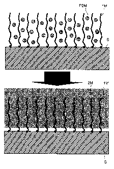
first material. This embodiment is illustrated
schematically in the attached Figure 1. This embodiment
may be performed, for example, in the following manner:
the first material is a polymer, for example an organic
polymer, for example electrografted onto the surface.
The second material is a metal deposited within the
polymer, for example in the form of a layer. The
polymer thus serves as "armouring" for attaching to the
metal layer. According to this embodiment, the first
material may be buried in the second material.
According to a second embodiment of the process of the
present invention, the first material may be attached
to the surface, for example by chemisorption or
CA 02516053 2005-08-12
B 14191.3 SL 22
electrografting, or simply deposited in a non-adhesive
manner, onto the surface in the form of a layering
material, and the second material formed within it
reinforces the attachment of the first material to the
surface by means of the interface connection created
between this second material and the surface: it is
stated, according to the invention, that the attachment
or deposit of the first material on the surface is
reinforced with the second material. This embodiment
ensures for the first material a more solid interface
than that existing between it when it is alone and the
surface. This embodiment may be illustrated in the same
manner as previously, but since the material of
interest is the first material, care will be taken to
ensure that it is not buried by the second material
during the formation of this second material from its
precursor. For example, since the second material, in
this case the reinforcing material, is deposited, for
example, by an electro-controlled reaction, the
electrical charge may advantageously be controlled
during its electrodeposition such that its growth
within the first material, or layerable material, takes
place only within it and does not bury the said
material. Via this embodiment of the invention, the
roots of the first material, which in this case is a
polymer, are, as it were, "dipped" in the second
material, which may preferably be chosen for its
interface compatibility with the surface. This example
is illustrated schematically in the attached Figure 2.
It is this second embodiment of the process of the
present invention which suggested to the present
inventors the name "electrochemical layering", layering
being a process used in botany to recreate roots from
CA 02516053 2005-08-12
B 14191.3 SL 23
branches by inserting them into the ground so that they
project from the soil.
According to one mode that is particularly preferred by
the present inventors, the process of the invention may
be performed on a surface that is a conductive or
semiconductive surface, the first material is a vinyl
polymer, the second material is a metal and the
precursor of this metal is an ion of this metal.
The step of inserting the precursor of the second
material into the first material according to the
process of the invention is a determining step.
Specifically, it is during this step that the precursor
of the first material is inserted into the second
material in order to be able thereafter to be converted
therein into the second material. Numerous techniques
falling within the context of the present invention for
this second step may be used. They range from simple
placing of the precursor of the second material in
contact with the first material placed on the surface,
for example by dipping the first material placed on the
surface into a suitable solution of the said precursor,
to more elaborate techniques such as the use of an
electrolytic bath.
If the first material does not allow easy insertion of
the precursor of the second material therein, or if
this insertion must be promoted, or even forced,
according to the invention, an insertion solution that
is both a solvent for or transporter of the precursor
of the second material, and a solvent and/or solution
that swells the first material may advantageously be
used, the said insertion solution comprising the
precursor of the second material.
CA 02516053 2005-08-12
B 14191.3 SL 24
For example, a solvent for the first material when it
is a polymer, is a solvent for this polymer.
The expression "solution which swells the first
material" means a solution that becomes inserted into
the first material and that deploys its structure to
allow the insertion into the first material of the
precursor of the second material that it contains . For
example, it may be an aqueous solution, for example
which hydrates the first material. Vinyl polymers that
are swollen by water, especially poly(4-vinylpyridine),
P4VP, which is insoluble in water, or polyhydroxyethyl
methacrylate, PHEMA, which is soluble in water and thus
also swollen by this solvent, are known. These polymers
may be used as f first material according to the present
invention.
This insertion solution is also a solution which makes
it possible to convey the precursor of the second
material within the first material. It will therefore
be a solution that allows a sufficient solubilization
or dispersion of the precursor for the implementation
of the present invention. Specifically, in the case of
insoluble salts of the second material, this solution
will preferably need to be able to disperse the
precursor of the second material sufficiently to be
able to insert it into the first material.
The insertion solution will thus be chosen as a
function of numerous criteria. Among these, mention may
be made of: as a function of the surface: for example
to avoid chemical interactions such as oxidation of the
surface during the implementation of the process; as a
function of the first material: so that this solution
CA 02516053 2005-08-12
B 14191.3 SL 25
does not remove this first material from the surface
onto which it has been deposited; as a function of the
precursor of the second material: it must allow its
dissolution, but also its conversion into second
material; as a function of the second material: it must
allow its formation within the first material, and
especially the implementation of its deposition
process, for example the electrodeposition of the
second material.
For example, since the prior art contains a wealth of
information firstly regarding the production of
metallic films by electrodeposition from aqueous
solutions, and secondly regarding their solubility
properties in water, the appropriate insertion solution
that is preferred according to the invention is an
aqueous solution, especially when the first material is
a polymer that can be swollen with water, for example
in the form of an electrografted armouring film. Other
insertion solutions and processes for inserting the
precursor of the second material into the first
material are described below. A person skilled in the
art will be able to select yet other suitable insertion
solvents for implementing the present invention, for
example with the precursors of the category of the
abovementioned "reinforcing" materials.
According to a third embodiment of the process of the
present invention, the step consisting in inserting the
precursor of the second material into the first
material placed on the said surface may be performed at
the same time as the step consisting in placing the
first material onto the said surface, by means of a
solution comprising both the said first material or a
precursor of the said first material, and the precursor
CA 02516053 2005-08-12
B 14191.3 SL 26
of the second material. This embodiment is particularly
advantageous, for example, when it is difficult to find
an insertion solution for swelling the first material
placed on the substrate. Thus, during the first step
consisting in placing the first material onto the
substrate, the precursor of the second material is
taken into the first material, and, when the first
material is placed on the surface, to apply the step of
the process of the invention consisting in converting
the precursor of the second material into the said
second material within the said first material.
The conversion step of the present invention is also
important, since it must allow the precursor of the
second material to be converted into the said second
material on the surface to be coated and within the
first material. The modes of this conversion have been
described above and are described in further detail
below. Preferably, the precursor of the second material
may be converted into the said corresponding second
material via a technique chosen from electrodeposition
and precipitation.
The process of the present invention may thus comprise,
once the surface that is intended to be coated and the
material of interest are determined, the selection of a
suitable complementary material, and also the selection
of the processes for depositing each of these two
materials according to the process of the present
invention, which will allow very strong adhesion of the
said material of interest to the said surface to be
produced.
In a first example of application of the invention, in
accordance with the first abovementioned embodiment, in
CA 02516053 2005-08-12
B 14191.3 SL 27
which it is desired to adhesively deposit a material of
interest, which is, for example, a metallic material
(A) classified above in the category of the second
material, onto the surface of a substrate, for example
of a semiconductor (B), the process of the invention
may comprise the following steps:
- selection of an armouring material, or first
material within the meaning of the present
invention, for example a polymer;
- selection of a process for depositing the
armouring material onto the surface, for example
the semiconductor (B); in this example, it is this
deposition process that will largely determine the
solidity of the connection between the material of
interest, metal (A), and the surface, in this case
the semiconductor (B). According to the invention,
a person skilled in the art may, of course, select
this process as a function of this solidity
criterion, but also on the basis of other
considerations, based especially on the thickness
of the desired layerable material, for example in
the form of a film, on the desired uniformity of
thickness of this material, on the cost etc. Very
solid fixing of the armouring material to the
surface, for example of the semiconductor B, may
be obtained, for example, if the armouring
material is a polymer that can be electrografted
onto the surface, for example the semiconductor B,
since this process makes it possible to produce
covalent chemical bonds between a polymer and a
conductor or a semiconductor;
CA 02516053 2005-08-12
B 14191.3 SL 28
- selection of a process for depositing the second
material within the meaning of the present
invention, in this case the metal A, such that it
is compatible with the process for depositing the
first material, the armouring material. The term
"compatibility" means that this process preferably
allows the growth of the reinforcing material
within the armouring material: this assumes
especially that the precursors of the second
material can first of all become inserted, i.e.
diffused, within, i.e. inside, the armouring
material, or first material, and that the process
can be applied thereto to allow the formation of
the second material within the armouring material;
implementation of the process of the invention as
defined above: if the second material is a metal,
metallic ions of this metal (A) will be used as
precursors of the second material, advantageously
dissolved in a solvent and/or a swelling agent for
the armouring material, for example the polymer,
to form the solution of the precursor of the
second material; this solution allows the
diffusion of the ions of the precursor within the
polymer, after which, for example, a process of
the galvanic type is applied, for example
electrodeposition (electroplating or
electrochemical deposition (ECD)), to form the
metal (A) within the polymer. Since this process
is electro-controlled, control of the charge
advantageously makes it possible to monitor that
the growth of the metal (A) takes place over the
entire thickness of the first material, in this
example of the polymer forming the armouring
material, before taking place over its surface.
CA 02516053 2005-08-12
B 1191.3 SL 29
In this way, the layerable material, i.e. the polymer,
or first material, is finally buried in the metal (A),
to which it served as "armouring" for attachment to the
metallic surface (B), by means of the interface
connection created between the armouring material and
the semiconductor (B): the deposit of the first
material, in this case the metal (A), on the surface,
in this case the semiconductor, is the said to have
been reinforced by the first material, in this case the
polymer. This application example is illustrated in the
attached Figure 1.
It is demonstrated, for example, in the "examples"
below that the adhesion of a layer of copper
electrodeposited onto a gold surface, or the adhesion
of a film of silver chloride onto a metallic surface is
thus, surprisingly, reinforced by a pretreatment that
provides a buried polymer reinforcement of the
interface between the two metals or between the metal
and the silver chloride.
In a second application example of the present
invention, in accordance with the abovementioned second
embodiment, in which it is desired to deposit a polymer
(P), as a layerable material of interest, onto a
surface, for example of a conductive substrate, for
example made of metal, the principle of the process is
based on the same steps as those described above,
except for the final implementation step. Specifically,
it is preferable in this final step, as stated above,
to control the growth of the second material within the
first material such that it does not bury this second
material.
CA 02516053 2005-08-12
B 14191.3 SL 30
It is demonstrated, for example, in the "examples"
section below that, by means of this second embodiment
of the invention, it is possible, unexpectedly, to
attach a film of poly(4-vinylpyridine) (P4VP) deposited
by centrifugation onto a gold surface, such that it
withstands drastic rinsing with one of its solvents,
whereas the film of P4VP alone, on the same surface, is
removed by the same rinsing in the absence of the
treatment according to the invention.
According to the invention, when the objective is that
the material of interest is the only one of the first
and second materials present at the surface when the
implementation of the process of the invention is
complete, the process will be adapted, as described in
the present text, either such that the first material
emerges from the second material, or such that the
second material immerses or covers the first material.
Advantageously, according to the invention, the
material of interest emerges or covers, depending on
the chosen embodiment of the invention, for example by
a thickness at least equal to 200 of the total
thickness formed by the two materials on the surface by
means of the process of the invention, following the
armouring or layering. The thickness of this emerging
portion is, obviously, adapted as a function of the use
for which this surface is intended.
The thickness of the coating formed by the first
material and the second material on the surface by
implementing the process of the invention is generally
between 1 nm and 100 ~zm. It obviously depends on the
nature of the materials used and on the desired type of
coating.
CA 02516053 2005-08-12
B 14191.3 SL 31
The coating obtained by means of the process of the
present invention thus comprises the first material and
the second material intermingled, with or without
chemical bonds or interactions between them, depending
on the chemical nature of the materials used.
The process of the present invention thus has numerous
applications that a person skilled in the art can
discover for himself on reading the present
description.
Among these applications, non-limiting examples that
may be mentioned include the following:
It allows interface reinforcement between a conductive
or semiconductive substrate and a metal, for example by
means of a polymer armouring pregrafted onto the
substrate in the manner illustrated in the attached
Figure 1. This application is advantageous for the
mechanical reinforcement of copper/antidiffusion layer
interfaces such as TiN, TaN, TiNSi, etc., especially in
the copper interconnection in microelectronics, in
particular according to the Damascene or Dual Damascene
processes.
It more generally offers an advantageous alternative to
adhesive sublayers in metal/metal, metal/conductive
polymer, conductive polymer/semiconductor or
metal/semiconductor interfaces.
For example, it also allows the deposition of very
adhesive organic layers onto conductive or
semiconductive substrates, especially for automotive
anticorrosion, optics, fashion articles, mechanical
CA 02516053 2005-08-12
B 14191.3 SL 32
lubrication, the deposition of hot-melt polymer layers
for "flip-chip" polymer applications, or alternatively
for functionalizing the sensitive part of a sensor. It
thus also relates to the use of the process of the
invention in an anticorrosion treatment of a metallic
surf ace .
For example, it also allows the deposition of very
adhesive organic layers such as the deposition of
biocompatible polymers and/or reservoirs for the
encapsulation and release of active molecules onto
conductive implantable objects, for instance imprints
for holding grafts in plastic surgery, or vascular
implants (stents), cochlear implant electrodes,
catheter guides (guidewires), orthopaedic implants and
especially hip prostheses, and dental implants. It thus
also relates to the use of the process of the invention
for the surface treatment of an object that can be
implanted into a body.
For example, it also allows the deposition of very
adhesive organic layers, such as the deposition of
biological macromolecules, or of macromolecules bearing
or encapsulating biological molecules, for instance
peptides, proteins, polysaccharides, oligonucleotides
or DNA or RNA fragments, especially for the manufacture
of DNA or protein biochips. It thus also relates to the
use of the process of the invention for the manufacture
of biochips.
The process of the present invention also allows the
manufacture of catalysts, for example by using as
precursor of the second material the abovementioned
metallic precursors or a mixture thereof, for example a
rhodium, platinum, palladium, cobalt, copper, etc.
CA 02516053 2005-08-12
B 14191.3 SL 33
precursor or a mixture thereof. In this application,
the first material may be one of those mentioned in the
present text, advantageously a polymer comprising
functions that can serve as ligands for complexing the
precursors of the second material, for instance poly(4-
vinylpyridine) (P4VP), and also any polymer bearing
cysteine groups, which may be used to bring about the
attachment, to a surface, of a salt of the catalyst,
for example palladium salts. After reduction within the
film of the first material, and possibly calcination of
the organic residue, the catalyst is obtained in its
metallic form, for example palladium metal, either in
film form or in the form of metallic aggregates. The
catalysts thus obtained have the advantage,
specifically, of initiating the deposition, for an
electroless process, of layers of different materials,
and especially of copper in applications related to
microelectronics (cf. for example: S. James, H. Cho et
al., "Electroless Cu for VLSI", MRS Bulletin, 20 (1993)
31-38) .
Detailed description of the invention
The idea underlying the establishment of the above
classifications is that processes are known for:
- constructing very solid interfaces between organic
materials, especially macromolecular materials,
and in particular polymers, and electrically
conductive and semiconductive surfaces, but the
list of organic materials concerned is limited;
- producing adhesive deposits of metals on other
metals, but again the list of entirely compatible
metal/surface couples is limited.
CA 02516053 2005-08-12
B 14191.3 SL 34
As indicated above, it is in fact known how to form
very solid chemical bonds between polymers and
electrically conductive or semiconductive surfaces via
electrografting of vinyl monomers or of cyclic
molecules that can be cleaved via nucleophilic or
electrophilic attack, for instance lactones and epoxy
compounds. It is also known how to perform the covalent
electrografting of functionalized aromatic nuclei,
starting with diazonium salts or sulphonium salts.
In a complementary manner, it is known how to produce
adhesive deposits of copper onto copper or onto most of
the transition metals via electrodeposition, for
example.
According to the invention, these deposition methods
are astutely used, in a crossed manner, to assist,
respectively, for example, the deposition of polymer
materials that cannot be electrografted onto certain
surfaces and also, for example, that of metals which
show poor adhesion to certain surfaces, for example to
conductive or semiconductive substrates of interest.
In addition, the present invention uses one of these
methods to assist the adhesion of materials that do not
conventionally form adhesive deposits on certain
surfaces, for example on conductors or semiconductors,
i.e. ionic solids.
It may be considered that the coating formed on the
surface by implementing the process of the invention is
a composite coating, since it has all the
characteristics thereof. Specifically, it generally
comprises a first material, which is preferably
CA 02516053 2005-08-12
B 1191.3 SL 35
organic, and a second material, which is preferably
mineral.
Thus, according to the invention, when the object is to
reinforce an interface between two materials, for
example a metal and a semiconductive substrate, as
represented in the attached Figure 1, an armouring
material thus constituting the first material within
the meaning of the present invention is, for example,
deposited by electrografting onto the said surface, for
example the surface of the semiconductive substrate,
and the other material, for example the metal,
constituting the second material within the meaning of
the present invention, is formed from its precursor
within the armouring material. The formation of the
second material, for example when it is a metal, is
advantageously obtained either by electrodeposition or
by chemical precipitation of the precursor of this
second material. In this example, when the operation is
complete, the armouring material is buried.
According to the invention, when the object is to layer
an organic material, constituting the first material
within the meaning of the present invention, onto a
surface, for example of a conductive or semiconductive
substrate, the reinforcing material, constituting the
second material within the meaning of the present
invention, is constructed within the said organic
material advantageously by electrodeposition, for
example by electrolysis, the said organic material
having been deposited onto the substrate by any
suitable means, for example by centrifugation, dipping
or spraying.
CA 02516053 2005-08-12
B 141.91 . 3 SL 36
The notion of adhesion of a coating to a surface is a
relatively subjective notion, since its assessment
depends on the stress to which the coating is
subsequently subjected under the working conditions.
Thus, for example, electrografting is a process known
to form polymer films on conductors or semiconductors
that withstand ultrasonic rinsing.
Any polymer deposited according to the present
invention onto a surface by simple centrifugation and
then reinforced with a second material within the
meaning of the present invention, for example a metal,
as shown in the attached Figures 1 and 4, forms a
reinforced coating whose adhesion to the surface is
improved compared with a deposit of the polymer alone,
without reinforcement on the said surface, without
anticipating the nature of the interface that has been
constructed between the reinforcing material and the
surf ace .
In many cases, this "resistance to removal" of the
polymer from the surface of the substrate may prove to
be sufficient, to the extent that the above list of
processes may be completed by considering that, for an
interface reinforcement as shown in the attached
Figure 1:
- the armouring polymer or macromolecular materials,
constituting the first material, may be deposited
by electrografting, centrifugation, dipping or
spraying;
- the reinforcing materials, constituting the second
material, may be deposited by electrodeposition or
chemical precipitation.
CA 02516053 2005-08-12
B 141,91 . 3 SL 3 7
It is for this reason that armouring materials and
layerable materials are placed in the same category
according to the initial classification: for example, a
polymeric or macromolecular organic material may be
said to be an "armouring" material if it is completely
buried after deposition of the reinforcing material,
and "layered" if it is not completely buried. In the
first case, the user will have chosen to bury it
because the reinforcing material is the material of
interest; in the second case, the user will have chosen
not to bury it in order to exploit its properties once
the reinforcement has been established.
Thus, for example, for the application of the present
invention to the adhesion of copper lanes onto TiN in
the Damascene process in microelectronics, the material
of interest is copper, whose interface with TiN it is
desired to improve for mechanical reasons: a film of
P4VP may be deposited onto TiN by electrografting or
centrifugation, before burying it in a layer of
electrodeposited copper as shown in Figure 1.
Conversely, high molecular weight P4VP may be deposited
onto a stainless-steel or graphite surface of high
surface area to manufacture a complexation filter that
may be used in a device for treating liquid effluents,
and to do this the surface is impregnated with P4VP and
this surface is then dipped into a solution containing
metal ions in order for them to become inserted into
the polymer film, and finally the copper thus trapped
is reduced such that the complexing pyridine groups are
still accessible above the reinforcing metal.
Moreover, if a first material placed on a surface via a
suitable process shows strong adhesion to the surface,
CA 02516053 2005-08-12
B 14191.3 SL 38
and if, independently of this first material, the
second material itself also shows strong adhesion to
this surface, the process of the present invention
advantageously makes it possible, as it were, to
cumulate the adhesions of these two materials on the
said surface. The present invention thus provides
ultra-resistant coatings, which have numerous
applications.
It is obvious that the burying of one or other of the
materials is not a necessity. The process of the
invention will, of course, be adapted according to the
use for which the coating is intended.
Irrespective of the considered application of the
present invention, in particular the selected
deposition processes, it is observed that the step of
depositing the armouring materials or materials to be
layered, which constitute the first material for the
purposes of the present invention, is always performed
before that of the reinforcing materials, which
constitute the second material for the purposes of the
present invention, as is shown in the attached Figures
1, 2 and 4.
Once the first material, for example a polymeric or
macromolecular organic material, is placed on a surface
of a substrate, for example a conductive or
semiconductive substrate, it is thus necessary for the
precursors of the second material, for example the
reinforcing material, to be able to be inserted, for
example by electrodeposition or precipitation, into the
first material.
CA 02516053 2005-08-12
B 141.91 . 3 SL 39
This insertion may take place by simple contact of the
precursor of the second material, preferably by means
of a solution thereof, with the first material placed
on the surface.
Thus, according to the invention, the solvent for the
insertion step is advantageously selected such that it
allows both the dissolution of the precursor of the
second material and, if necessary, the swelling and/or
dissolution of the first material, for example the
organic armouring film or film to be layered, so as to
optimize the insertion of the precursor.
For example, in the case where the first material is a
polymer, the solution containing the precursor of the
second material may advantageously be selected from
liquids that swell but are not solvents for the polymer
or solvents for the polymer. In particular, if the
first material is a polymer that has been
electrografted, it is possible to select swelling
liquids that are not solvents for the polymer, but also
solvents for the polymer since this polymer cannot be
detached from the surface with these solvents, and thus
by the solution of the precursor that these solvents
form.
On the other hand, if the first material, for example
an organic material, has been deposited by
centrifugation or dipping to form armouring or
layering, a solution consisting of a simple swelling
solvent for the polymer, which has as little solvent
nature as possible, will preferably be used so as to
avoid washing the polymer off the surface onto which it
has been predeposited.
CA 02516053 2005-08-12
B 141,91 . 3 SL 4 0
For example, in the case where the first material is
P4VP, this polymer may be readily electrografted or
deposited, by centrifugation or dipping, from a
solution in dimethylformamide (DMF), which is a good
solvent for the polymer. Once the solvent has been
evaporated off, it is possible, in either case, to dip
the surface on which this first material has been
placed in an aqueous solution, since water is a good
swelling agent but a poor solvent for P4VP.
Under these conditions, according to the invention, the
insertion of the precursor of the second material, for
example ions, may take place "naturally", by simple
diffusion into the polymer, for example by dipping into
a solution containing the precursor ions of the second
material. This diffusion is generally proportionately
faster the more concentrated the precursor bath.
The inventors have thus observed that a film of P4VP on
stainless steel approximately a hundred nanometres
thick is saturated with copper ions within a few
minutes at room temperature when the surface is dipped
into a solution containing 20 g/1 of copper sulphate.
Advantageously, the saturation of the first material,
for example in the form of a film, with the precursor
of the second material may also be facilitated by the
presence within the first material of functional groups
capable of retaining the precursor of the second
material, for example by complexing it when it is in
the form of precursor ions. This retention may be
provided by means of ionic bonds, dative bonds or
interactions of Lewis acid-Lewis base type, covalent
bonds or hydrogen bonds, or alternatively by mechanical
retention (absence of possibility of diffusion out of
CA 02516053 2005-08-12
B 14791.3 SL 41
the first material), for instance when the precursor of
the second material is precipitated within the first
material.
For example, in the abovementioned example, the cupric
ions, forming the precursor of the second material
which is copper, are very efficiently complexed by the
lone pairs of the pyridine nitrogens of the P4VP
forming the first material.
Advantageously, the first material for example a
polymer, may thus be chosen as a function of the
precursor of the second material, especially when this
second material is in the form of ions, such that this
first material contains groups that complex the
precursor satisfactorily in order for it to remain
inserted within the polymer.
Once the precursor of the second material is inserted
in the first material, for example in the polymer film,
it is advantageously possible to perform either its
electroreduction or its precipitation, within the film
so as to form the said second material within the said
first material.
For example, if the object is to produce armouring of
the second material using the first material, for
example in the case of interface reinforcement in the
Damascene process, electroreduction of the precursor of
the second material, for example of copper, may
advantageously be performed in the same bath as that
used to saturate the film with the said precursor,
since the object in this example is that the growth of
the reinforcing material continues beyond the thickness
CA 02516053 2005-08-12
B 14191.3 SL 42
of the armouring material. Figures 1 and 4
schematically illustrate this example.
For example, if the object is, on the contrary, to
layer an organic film forming the first material, the
surface bearing the organic film swollen with precursor
ions may be advantageously removed from the precursor
solution and then dipped in an electrolytic bath not
containing the precursor ions.
In this latter example, according to the present
invention, the presence of functional groups that
complex the ions in the film will advantageously slow
down the exit of the ions from the film into the new
solution since the inversion of the concentration
gradients between the precursor inserted into the first
material and the precursor solution, and between the
precursor inserted into the first material and the
solution formed by the electrolytic bath without
precursor results in inversion of the precursor
diffusion currents. The inventors have observed,
specifically, by infrared reflection spectroscopy
(IRRAS) that a P4VP film 100 nm thick on stainless
steel, saturated with cupric ions, conserves its ions
even after a residence of several hours in a saturated
aqueous sodium chloride solution.
If the second material is formed from its precursor by
electrodeposition, the amount of the second material
deposited into the first material, for example of a
film to be layered, may advantageously be controlled by
controlling the electrodeposition potential. In
addition, the fact that the second material is prepared
exclusively from its precursor inserted into the first
material and in an electrolytic bath not containing any
CA 02516053 2005-08-12
B 14~-91.3 SL 43
precursor of the second material advantageously ensures
that the film to be layered is not buried by the second
material. This particular embodiment of the present
invention thus makes it possible to ensure, when
necessary, that the first material, when it is a
layering material, is not buried by the second
material.
As is seen in the present description, the first
material may be placed on the surface by means of any
process known to those skilled in the art. The term
"placed" is used in the present text to denote in
general any type of deposition known to those skilled
in the art, for example spraying, dipping,
centrifugation, electrografting, electrodeposition,
etc. According to the invention, the process for
placing the first material on the surface will be
chosen by the operator as a function especially of the
nature of the surface and of the intended use of the
coating manufactured by implementing the process of the
invention, in particular of the type of adhesion
desired on the surface.
According to the invention, irrespective of the process
chosen to place the first material onto the surface,
the first material may preferably be placed onto the
surface to be coated in the form of a film or layer,
and more preferably in the form of an organic film or
layer.
Preferably, according to the invention, and when this
is possible on account of the nature of the surface,
the first material may be placed onto the surface to be
coated by means of electrografting. The electrografting
may, specifically, be advantageously used when the
CA 02516053 2005-08-12
B 14191.3 SL 44
surface that is intended to be coated by means of the
process of the invention is a conductive or
semiconductive surface. It allows strong attachment of
the first material onto the surface to be obtained.
According to the invention, the first material may be
advantageously prepared from a precursor thereof,
referred to hereinbelow as the precursor of the first
material, chosen from the group consisting of activated
or cyclic vinyl monomers, functionalized or non-
functionalized diazonium salts, functionalized or non-
functionalized sulphonium salts, functionalized or non-
functionalized phosphonium salts and functionalized or
non-functionalized iodonium salts. Specifically, the
first material may advantageously be obtained from one
or more of these precursors, for example by
electrografting reaction on the surface, for example of
an electrically conductive or semiconductive support.
Specifically, the electrografting of these precursors
on the surface advantageously results in a film of the
first material being placed on the surface within the
meaning of the present invention.
According to the invention, the first material may be
advantageously obtained from a precursor thereof, known
as the precursor of the first material, chosen from the
group consisting of activated vinyl monomers, cyclic
molecules that are cleavable by nucleophilic attack,
and diazonium salts.
For example, the activated vinyl monomers that may be
used in the present invention may be those having the
structure (I) below:
CA 02516053 2005-08-12
B 14191.3 SL 45
R2
R3 R4 (I)
in which R1, R2, R3 and R4 are organic groups chosen,
independently of each other, from the group consisting
of the following organic functions: hydrogen (H),
hydroxyl (-OH) , amine (for example -NHX, with x = 1 or
3), thiol (-SH), carboxylic acid (-COOH), ester (for
example -COORS, with RS being a C1 to C6 alkyl) , amide
(for example -C(=O)NHy, with y = 1 or 2), imide, imido-
ester, acid halide (for example C(=O)X, X - F, Cl, Br
or I), acid anhydride (for example -C(=O)OC(=O)),
nitrile, succinimide, phthalimide, isocyanate, epoxide,
siloxane (for example -Si(OH)Z, with z - 1 or 3),
benzoquinone, benzophenone, carbonyldiimidazole, para-
toluenesulphonyl, para-nitrophenyl chloroformate,
ethylenic, vinyl, aromatic, for example toluene,
benzene, halobenzene, etc.
In addition, at least one from among R1, R2, R3 and R4
may be a functional group that can complex rations and
especially reducible metal rations, for instance
copper, iron, nickel, etc. chosen, for example, from
the group consisting of amines, amides, ethers,
carbonyls, carboxyls and carboxylates, phosphines,
phosphine oxides, thioethers, disulphides, ureas, crown
ethers, crown azas, crown thins, cryptands,
sepulcrates, podands, porphyrins, calixarenes,
pyridines, bipyridines, terpyridines, quinolines,
ortho-phenanthroline compounds, naphthols,
isonaphthols, thioureas, siderophores, antibiotics,
ethylene glycol and cyclodextrins.
CA 02516053 2005-08-12
B 141.91 . 3 SL 46
The film of the first material may also be obtained
from substituted and/or functionalized molecular
structures from the abovementioned functional groups.
Any compound, of molecular or macromolecular size,
bearing vinyl groups such as those indicated above, for
instance telechelic compounds with vinyl end groups,
and in particular telechelic mono- and dimethacrylate,
for instance polyethylene glycol dimethacrylate or
polydimethylsiloxane dimethacrylate, or alternatively
vinyl macromers, i.e. macromolecular compounds mono- or
polyfunctionalized with vinyl groups, may also be
suitable as precursors of the first material. This last
category includes, for example, polymers (vinyl
polymers, for instance polyvinyl alcohol, polyacrylic
,_ 15 acid or polymethacrylic acid, polyallylamine, etc.;
polycondensates, for instance polylactic acid,
polyglycolic acid, polyortho esters, polyamides etc.,
polyethyleneimine etc.), or copolymers, in which all or
some of the pendent functional groups have been
functionalized with vinyl groups. It is thus possible,
for example, to obtain a precursor of the first
material by reacting methacryloyl chloride or glycidyl
methacrylate on all or some of the OH or NH functional
groups of a polymer, for instance polyvinyl alcohol or
polyallylamine, and produce, respectively, a polyvinyl
alcohol or a polvallvlamine functionalized with
methacrylate groups. More generally, non-polymer
macromolecules, for instance polysaccharides (dextrans,
celluloses, heparin, chitosans, etc.), proteins
(fibrin, caseine, etc.), oligonucleotides (single-
stranded and double-stranded DNA or RNA, etc.),
peptidoglycans, in which all or some of certain of
their functional groups have been functionalized with
vinyl groups, may constitute precursors of the first
material. A dextran-GMA functionalized with glycidyl
CA 02516053 2005-08-12
B 141.91 . 3 SL 47
methacrylate groups is obtained, for example, from a
dextran of mass M - 15 000 and from glycidyl
methacrylate (2,3-epoxypropyl methylpropenoate),
according to the protocol described in W.N.E. by
van Dijk-Wolthuis, O. Franssen, H. Talsma, M.J. van
Steenbergen, J.J. Kettenes-van den Bosch, W.E. Hennink,
Macromolecules, 1995, 28, 6317. A film 200 nm thick is
obtained by electrografting onto gold under
voltammetric conditions with 15 sweeps from Einitial -
-0. 6 V/ (Ag+/Ag) to Efinal = -2 . 8 V/ (Ag+/Ag) at a speed of
100 mV/s, by dipping a gold leaf, used as working
electrode in a 3-electrode assembly, into a solution
obtained by dissolving 0.25 g of dextran-GMA in 50 ml
of DMF at 102 mol/1 of TEAP (the solution is thus about
3.3x10⁻⁴ mol/1 of dextran-GMA). Due to the fact that
when deposited by electrografting, this film adheres
very strongly to the surface and especially withstands
ultrasonic rinsing. It thus constitutes a first
material of choice, which can receive the precursors of
a second material, and in particular metal salts,
especially by dipping the leaf in a solvent or a
swelling agent containing these metallic precursors.
Finally, the film of the first material may also be
obtained from mixtures of the abovementioned chemical
precursor compounds, so as to obtain copolymer films,
possibly initiated with diazonium salts, constituting
the first material within the meaning of the present
invention.
For example, according to the invention, when the first
material is a polymer obtained by polymerization of a
vinyl precursor monomer, it may advantageously be
chosen from the group consisting of vinyl monomers, for
instance acrylonitrile, methacrylonitrile, methyl
CA 02516053 2005-08-12
B T4191.3 SL 48
methacrylate, ethyl methacrylate, butyl methacrylate,
propyl methacrylate, hydroxyethyl methacrylate,
hydroxypropyl methacrylate, glycidyl methacrylate,
acrylamides and especially amino- ethyl, propyl, butyl,
pentyl and hexyl methacrylamides, cyanoacrylates,
cyanomethacrylates, polyethylene glycol dimethacrylate
and more generally telechelic diacrylates or
dimethacrylates, acrylic acid, methacrylic acid,
styrene, para-chlorostyrene, N-vinylpyrrolidone,
4-vinylpyridine, 2-vinylpyridine, vinyl halides,
acryloyl chloride, methacryloyl chloride,
divinylbenzene (DVB), pentaerythritol tetramethacrylate
and more generally acrylate-based, methacrylate-based
or vinyl-based crosslinking agents, and derivatives
thereof.
For example, the cyclic molecules cleavable by
nucleophilic attack which may be used in the present
invention may be those having the structure (II) below:
(II)
in which R1 and Rz are independently as defined above,
and in which n, m and p are each independently integers
from 0 to 20. Included in this category, for example,
are epoxides (R1 being an alkyl group as listed above,
R2 - H, n = 1, m = 0, p = 1), such as ethylene oxide (R1
- H, Rz - H) ; lactones (R1 and Rz being alkyl groups as
listed above, m = 1, p = 1), for instance butyrolactone
(n = 2% R11 = H~ Rzl = H~ Rlz = H~ Rzz = H~ m = 1~ P = 1)
s-caprolactone (n - 5: Rli - H, Rzi - H, 1 <_ i <_ 5; m =
1, p = 1), etc.
CA 02516053 2005-08-12
B 141-91 . 3 S L 4 9
For example, the diazonium salts that may be used in
the present invention may be those having the structure
(III) below:
X , N2+-~-R3 (III)
in which R3 is as defined above,
in which ~ is an aromatic nucleus, and
in which X is a negatively charged counterion chosen,
for example, from the group consisting of a
tetrafluoroborate, a halide, a sulphate, a phosphate, a
carboxylate, a perchlorate, a hexafluorophosphate, a
ferrocyanide or a ferricyanide.
Examples of diazonium salts that may be used to
constitute the first material within the meaning of the
present invention are, for example, 4-nitrophenyl-
diazonium tetrafluoroborates (in which the nitro group
can be reduced to amine with complexing properties),
4-carboxybenzenediazonium tetrafluoroborate (R3 - COOH)
and more generally benzenediazonium tetrafluoroborates
para-substituted with groups having complexing
properties, and especially those bearing carboxylic
acid groups ((-CH2)n-COOH, with n being an integer
ranging from 1 to 10), EDTA (ethylenediaminetetra-
acetate) and similar ligands, etc.; bipyridine,
quinolines, amino acids and proteins, mono- and
polysaccharides, etc.
All these chemical compounds that are precursors of the
first material may, of course, be used alone or as a
mixture depending on the objective of the operator
implementing the invention.
CA 02516053 2005-08-12
B 14191.3 SL 50
The first material will be chosen, of course, as a
function of numerous criteria, especially the chemical
nature of the surface, the material of interest, the
chemical nature of the second material if this is not
the first material, and also the intended use of the
coating manufactured in accordance with the process of
the present invention. For example, in the case where
it is desired to reinforce a metallic layer by
implementing the process of the invention, precursor
monomers of a first material in polymer form may
advantageously be used, the said polymer advantageously
being bearers of functional groups allowing the
complexation of the precursor of the second material,
for example when this material is in the form of ions.
All these chemical compounds that are precursors of the
first material may advantageously be used directly on
the surface, for example when the initiation of their
polymerization is brought about directly by the
metallic surface placed under potential in the manner
shown in the attached Figure 3; or alternatively as a
mixture with electro-activatable initiators, which,
once reduced or oxidized on the surface, themselves
initiate the polymerization: diazonium salts,
sulphonium salts, phosphonium salts, iodonium salts,
peroxodisulphates, persulphates, thiosulphates,
ferrocene, carboxylic acids and especially benzoic
acids, peracids, etc. and in general any electroactive
compound leading to the formation of initiating
radicals once reduced or oxidized.
The step of the process of the invention that consists
in depositing the first material onto the surface may
be a step consisting in obtaining an organic layer or
film of the first material from its abovementioned
CA 02516053 2005-08-12
B 14191.3 SL 51
chemical precursor compounds. It may advantageously
take place, for example, by electrolysis in totally or
partially organic medium, according to different
protocols for placing under potential known to those
skilled in the art. Among these, mention may be made of
the following: nominal current under intentiostatic
conditions, voltammetry, number of sweeps under
voltammetric conditions, potential multipulses,
intentiostatic jump, potentiostatic jump, etc.
The medium used to place the first material onto the
surface by these techniques may comprise, for example,
an organic solvent, for instance dimethylformamide
(DMF), acetonitrile, water, alcohols or a mixture of
these solvents, and optionally a support electrolyte
such as tetramethylammonium, tetraethylammonium,
tetrapropylammonium or tetrabutylammonium perchlorate
(TMAP, TEAP, TPAP or TBAP, respectively), lithium,
sodium or potassium perchlorate, sodium or potassium
chloride, sodium or potassium nitrate and more
generally any salt that is substantially soluble in the
electrosynthesis medium.
By way of example, a film of poly(4-vinylpyridine)
(P4VP) on gold 20 to 40 nm thick, which may be used in
the present invention, may be obtained by performing
voltammetric sweeps from -0.7 to -2.9 V/(Ag+/Ag) at
200 mV/s on a gold surface dipped into a solution
containing 95% by volume of 4-vinylpyridine in DMF, in
the presence of 5x10⁻² mol/1 of TEAP. The window of
thickness mentioned corresponds to different numbers of
voltammetric sweeps, the median thickness (30 nm) being
obtained with 50 sweeps. All factors being otherwise
equal, a film 100 to 150 nm thick is obtained by adding
to the above solution 5% by volume of pentaerythritol
CA 02516053 2005-08-12
B 14191.3 SL 52
tetramethacrylate, and by simultaneously copolymerizing
these two monomers.
Also by way of example, a film of polymethacrylonitrile
(PMAN) on gold about 50 nm thick, which can be used in
the present invention, is obtained, in a similar
manner, by performing 10 voltammetric sweeps from -0.5
to -2 . 7 V/ (Ag+/Ag) at 50 mV/s on a gold surface dipped
into a solution containing 2.5 mol/1 of
methacrylonitrile in DMF, in the presence of 5x10⁻²
mol/1 of TEAP. The nitrile groups of the polymer formed
are identified by the band at 2235 cm-1 in IRRAS.
Also by way of example, the formation of an
electrografted film of polyhydroxyethyl methacrylate
(PHEMA) on gold about 40 nm thick, which can also be
used in the present invention, is obtained by
performing 10 voltammetric sweeps from +1.0~ to
-3.0 V/(Ag+/Ag) at 50 mV/s on a gold surface dipped
into a solution containing 0.4 mol/1 of hydroxyethyl
methacrylate in DMF, in the presence of 5x10⁻² mol/1 of
TEAP (tetraethylammonium perchlorate).
Also by way of example, a 300 nm film of PHEMA, which
can be used in the present invention, on 316L stainless
steel is obtained by performing 40 voltammetric sweeps
from -0.6 to -3.0 V/(Ag+/Ag) at 100 mV/s on a
stainless-steel surface dipped into a solution
containing 3.5 mol/1 of hydroxyethyl methacrylate
(HEMA) in DMF, in the presence of 2.5x10⁻² mol/1 of
NaN03 and 10-2 mol/1 of 4-nitrophenyldiazonium
tetrafluoroborate.
Also by way of example, an ultrathin covering grafted
film of alkylbenzene (R-~-) with an estimated thickness
CA 02516053 2005-08-12
B 14191.3 SL 53
of less than 50 nm (and virtually proportional to the
size of the alkyl group R), which can be used in the
present invention, is obtained on a titanium nitride
surface by performing 3 voltammetric sweeps from +1.15
to -1.52 V/(Ag+/Ag) at 20 mV/s on a TiN leaf dipped
into a solution containing 5x10⁻³ mol/1 of
alkylphenyldiazonium tetrafluoroborate in acetonitrile,
in the presence of 5x10⁻² mol/1 of TEAP.
The concentration conditions of the precursor of the
first material within the meaning of the present
invention, for example monomer or diazonium salt, are
variable from one precursor to another and depend on
the objective of the operator implementing the
invention. Specifically, the concentration of precursor
of the first material has an impact on its arrangement
on the surface in the first step of the process of the
invention, but also on the other steps of the process
of the invention, i.e. on the steps of inserting the
precursor of the second material into the first
material and of forming the second material from its
precursor, and also on the properties of the coating
obtained.
However, concentrations of between 0.1 and 10 mol/1 and
in particular between 0.1 and 5 mol/1 for the monomers,
and 10-4 and 1 mol/1, and in particular 10-3 and
0.1 mol/1 for the diazonium salts, may be considered as
preferential. A person skilled in the art will readily
be able to adapt these concentration ranges to the use
that he will make of the present invention.
All these chemical compounds that are precursors of the
first material have in common the fact that they
advantageously result in the formation of structures of
CA 02516053 2005-08-12
B 141.91 . 3 SL 54
"brush" type, as sketched at the top of the attached
Figure 1, which are well configured to serve as
armouring structures for the deposition of ordinary
non-adhesive solids, in accordance with the process of
the present invention.
The scheme of Figure 1 gives an indication of what may
be obtained at a high degree of grafting, i.e. the
number of polymer stems per unit area.
With a lower degree of grafting, "hair" or polymer
structures layered on the surface will usually be
obtained, the armouring properties of which may be
substantially poorer than those of brush structures,
but which generally satisfy the desired function in
accordance with the present invention.
In general, whether it is a matter of performing the
electrografting of precursor chemical compounds of the
first material of diazonium salt type or of monomer
type, the degree of grafting may advantageously be
adjusted by the amount of current passed through the
electrical circuit used. Specifically, all these
electrografting reactions are electro-initiated
reactions, in which only the step of attachment of the
first precursor consumes an electron, as is shown in
the attached Figure 3, which is equivalent to it
occupying a site of the surface. The growth, when it
exists, i.e. in the case of the monomer precursors of
polymers, is then purely chemical. The current passed,
or more specifically the charge passed, i.e. the
integral charge of the current, is thus linked to the
number of sites of the surface that have been occupied,
and thus to the morphology of the film formed. A person
skilled in the art can thus readily predetermine the
CA 02516053 2005-08-12
B 14191.3 SL 55
conditions under which he obtains a film of a given
morphology by measuring the degree of grafting
obtained, for example by electrochemical impedance
spectroscopy, according to the operating conditions, in
order to find the solution that is best adapted to the
application he is making of the present invention.
When the layer of the first material is deposited
according to one of the abovementioned techniques, the
second material may be inserted into this layer forming
the first material in accordance with the process of
the invention. Numerous techniques included in the
context of the present invention may be used for this
step. However, the inventors have noted that the
following techniques are particularly advantageous for
implementing the present invention.
Thus, according to one preferred embodiment of the
invention, the second material is inserted into the
first material using a solution of ionic precursors of
this second material. It may be, for example:
an electrolytic bath, for initiating the formation
of the second material within the first material
by electrodeposition, such as a bath of metallic
salts, which is suitable, for example, for the
deposition of copper, zinc, gold, tin, etc.; a
bath of charged polymers or polyelectrolytes, etc.
The bath may optionally contain a mixture of these
precursors, so as to produce alloys (several
metallic precursors) or organometallic composites
(metallic precursors + organic precursors);
- a precipitation bath, for precipitating the second
material from its precursor in the form of an
CA 02516053 2005-08-12
B 14191.3 SL 56
insoluble salt. In this case also, the bath may
optionally contain several types of precursors, so
as to produce coprecipitations of several
different second materials in the first material.
In the two cases, an important step will consist in
ensuring the penetration of the ionic precursors into
the organic armouring film.
This assumes that the first material, for example an
organic film, can receive this precursor of the second
material. If the first material readily receives the
precursor of the second material within it., the
following precautions will not necessarily be required.
On the other hand, if the first material receives the
precursor of the first material less readily or with
difficulty, it may be necessary to make this insertion
possible or to improve it. To do this, various
solutions may be adopted depending on the origin of
this difficult insertion. If the origin of this
unfacilitated insertion is steric bulk due to the
conformation of the first material, which usually
appears to be the case, the solution may consist in
swelling the first material using a suitable solvent.
In the case where the first material is a polymer, this
suitable solvent may be, for example, a solvent for the
said polymer and/or a solvent or solution for
"swelling" the said polymer.
Advantageously, the first material may be at least
swollen by the liquid phase containing the ionic
precursors of the second material.
CA 02516053 2005-08-12
B 14191.3 SL 57
For example, when the precursor of the second material
is of ionic nature, the solution containing it for its
insertion into the first material is preferably a
liquid of relatively high dielectric permittivity,
which excludes highly apolar solvents.
Since there is a wealth of information in the prior art
regarding the production of metallic films by
electrodeposition from aqueous solutions, and also
regarding the solubility properties (solubility
product) in water, the electrografted armouring films
which are swollen by water are advantageously suitable
in the present invention.
P4VP, as a first material, for example, is swollen with
water, as indicated by the result of the attached
Figure 5A: immersion of a P4VP film 100 nm thick for
10 minutes into an aqueous solution containing 5 g/1 of
copper sulphate leads to the formation of
pyridine/cupric ion complexes, which are particularly
visible in infrared (IRR.AS), which shows the
penetration of the cupric ions into the film, whereas
the water is not a solvent, but only a swelling agent,
for the P4VP.
The same film, removed from the copper sulphate
solution and dipped in water, without CuS04, for
minutes, removed again and then dried, gives the
same spectrum as that in the attached Figure 5B,
30 proving that the cupric ions can even be "trapped" in
an electrografted film. This result can undoubtedly be
linked to the fact that the electrografted film
contains complexing groups, and that the
pyridine/cupric ion complexes formed are more stable
than water/cupric ion complexes. The inventors have in
CA 02516053 2005-08-12
B 14191.3 SL 58
fact noted that the ions may be "removed" from the film
by immersion in a solution containing ammonia, which
leads to particularly stable complexes with cupric
ions, which are manifestly more stable than the
pyridine/cupric ion complexes initially formed in the
film.
The same type of penetration into the first material,
in the form of an electrografted polymer, may be
obtained if it is performed in a genuine solvent for
the said polymer: thus, the penetration of cupric ions
or of zinc(II) ions into a P4VP film or into a
polyacrylonitrile (PAN) film is very readily performed
using a solution of cupric or zinc(II) ions
(respectively) in DMF, which is an organic liquid in
which P4VP and PAN are soluble (in solution).
In general, organic solvents with a permittivity lower
than that of water do not make it possible to prepare
insertion solutions that are as highly concentrated in
precursor ions of the second material as is possible in
water, since the ions therein are less soluble than in
water. However, this drawback may be offset by using
particular organic counterions, such as organic
counterions that are very soluble in the organic phase,
for instance those used in phase-transfer catalysts or
in liquid/liquid extraction processes: fatty acid
carboxylates (soaps), alkyl sulphonates, alkyl
phosphonates, alkyl phosphates etc., which, however,
makes the formulation more expensive. The inventors
have observed that the penetration of the precursor
ions into the electrografted films is generally slower
when the concentration in the dipping bath is lower.
CA 02516053 2005-08-12
B 14191.3 SL 59
For example, in the case where it is difficult to find
a liquid that is a good swelling agent for the first
material and in which the precursors of the second
material can also be dissolved, the third embodiment of
the present invention will advantageously be used. This
third embodiment may be implemented, for example, by
using a solution for grafting the first material onto
the surface containing both the precursor of the first
material and the precursor of the second material. The
electrografting of the first material onto the surface
may be performed in the manner described above or by
any other suitable technique . Once the grafting of the
first material has been performed, a polymer film
already containing the precursor of the second material
is obtained. Thus, according to this third embodiment,
the step of inserting the precursor is performed
simultaneously with the step of placing the first
material on the surface of the substrate. This
embodiment, which avoids an independent step of
inserting the precursor of the second material into the
first material and also possible washing of the surface
before converting the precursor into the second
material, can allow time to be saved in the application
of the process of the invention. The step of converting
the precursor of the second material into the second
material may be performed as in the other embodiments
of the present invention.
Once the penetration of the precursor ions of the
second material into the electrografted film has been
performed, according to the invention, the said
precursor ions of the second material inserted into the
first material are converted into the said second
material such that this second material becomes formed
CA 02516053 2005-08-12
B 14191.3 SL 60
on contact of the said surface to be coated and within
the said first material placed on the said surface.
According to the invention, this conversion may be
performed in the same solution as that used to insert
the precursor of the second material into the first
material, or in another solution.
For example, when the second material is obtained by
electrodeposition of its precursor into the first
material, this may be performed using an electrolytic
bath containing the precursor ions. The electro-
deposition of the second material into the first
material may be performed according to a procedure
known to those skilled in the art for the preparation
of electrolytic deposits. If it is desired to "sub-
merge" the electrografted film in the electrodeposited
material, it is preferable for the precursor ions of
the second material that are in the electrografted film
to also be present in the solution for converting it.
Specifically, when the cathodic deposition begins, it
leads to the manufacture of a metallic layer within the
film, first via the bottom, on the surface to be
coated: the ions of the film are attracted by the
bottom, which attracts the ions of the solution into
the film to continue the growth by deposition of the
second material in the film.
According to the invention, the reinforcing bath may
thus be the same as the dipping bath which allowed the
film to be filled with the precursor ions. Thus, it
will advantageously be possible to dip the "empty" film
constituting the first material in the dipping
solution, wait for the ions to diffuse into the
CA 02516053 2005-08-12
B 14191.3 SL 61
electrografted film, and then activate the protocol for
electrodeposition of the second material in the film.
According to this protocol of the invention, a high-
quality copper deposit, for example, reinforced with a
200 nm P4VP film on nickel, is obtained by performing
the following steps: (i) dipping the film in an aqueous
solution containing 50 ml of distilled water, 11 g of
[CuS04 ~ 5H20] , 3 g of HZS04 (d = 1 . 83 ) and 6 mg of NaCl,
for 30 minutes; (ii) electrolysis for 15 seconds at the
equilibrium potential, and then for 1 minute at
-0.5 V/(Ag+/Ag) (current density of between 2 and
4 A/dm2), with magnetic stirring.
For example, when the second material is obtained from
its precursor by precipitation, this precipitation may
be performed using a bath containing the counterions
for precipitating a salt of the precursor of the said
second material. This procedure is, of course,
preferably performed with a bath that is different from
the one used for dipping, so as to avoid precipitation
in all of the reinforcing bath.
For example, by means of this protocol, a deposit of
silver chloride on a nickel surface, reinforced with
P4VP, is obtained by dipping a nickel leaf bearing an
electrografted P4VP film 200 nm thick into a 5 g/1
silver nitrate solution for 30 minutes, followed by
removing the leaf and dipping it for a few minutes,
after rinsing with deionized water, into a 10 g/1
sodium chloride solution.
The same operation performed, for example, on a nickel
leaf bearing no electrografted P4VP film does not lead
to any deposit after treatment with the NaCl solution.
CA 02516053 2005-08-12
B 14T91.3 SL 62
Now that the principle of forming the deposit within
the electrografted armouring organic coating has been
described in detail, advantageous variants of the
S process of the invention are described below:
the penetration of the precursor of the second
material into the first material, if the precursor
of the second material is in the form of precursor
cations, may advantageously be accelerated if it
is performed at a slightly cathodic potential,
which will allow the cations to be attracted into
the film. The only problematic parameter is that
of being able to find a potential that is
sufficiently cathodic to ensure electrostatic
attraction and a migration current, and
sufficiently sparingly cathodic to perform the
reduction of these ions of the precursor in order
to form the second material, unless it is desired
to perform the two steps simultaneously;
- the conversion of the precursor of the second
material, when it consists of a reduction of
precursor ions, may advantageously be performed
via the chemical redox route, instead of an
electrodeposition, by dipping the electrografted
organic film, constituting the first material,
containing the precursor ions, into a solution of
chemical reducing agents. For example, a film of
reinforced silver on nickel is obtained by dipping
a nickel leaf covered with an electrografted
200 nm P4VP film into a 5 g/1 silver nitrate
solution for 30 minutes, followed by dipping it
for a few minutes, after rinsing with deionized
water, into a glucose solution heated to 80°C.
CA 02516053 2005-08-12
B 1.4391.3 SL 63
However, it will be noted that this type of
protocol does not generally allow the armouring
layer to be completely buried in the second
material, given the absence of ions of the
precursor of the second material in the solution
to make up the amount, by diffusion into the
electrografted film, of the precursor ions
consumed by the process for converting the
precursor of the second material into the second
material.
Electrografting makes it possible, for example, to
produce, by means of the formation of covalent bonds at
the surface/first material interface, particularly
solid armouring between the surface and the
complementary material.
As indicated above, a deposit of the first material on
the surface leading to a weaker bond than an electro-
grafting of the said first material may also be
performed, by means of the process of the invention.
This leads, for example, to armouring, consisting of
the first material, which is intrinsically less solid
but, nevertheless, acceptable depending on the intended
application.
This may be performed by depositing the first material,
for example in the form of an organic coating, via
processes that are simpler than electrografting, such
as dipping ("dip-coating"), centrifugation ("spin-
coating") or spraying. These three deposition modes are
well known to those skilled in the art.
It is known, for example, that it is possible to
control the thickness of an organic deposit by
CA 02516053 2005-08-12
B 14191.3 SL 64
centrifugation by adjusting the concentration of the
polymer in the deposition solution, the speed of
rotation of the device and the operating time. In the
dipping protocol, it is the speed of descent, but above
all of ascent, of the object in the polymer solution
that replaces the rotational speed parameter of
centrifugation, and enables good control of the
thickness of the polymer. In the spraying protocol, the
thickness may be controlled by controlling the size of
the drops, their ejection speed (via the geometrical
characteristics of the nozzle and the pressure of the
carrier gas, especially) and the distance between the
nozzles and the surface to be treated. These factors
fall perfectly within the implementation of the present
invention since they make it possible to adjust the
deposition of the first material onto the surface in
the process of the invention.
The inventors have,.for example, obtained a deposit of
silver chloride on a nickel surface, reinforced with
P4VP, by first producing a P4VP deposit by dipping the
leaf in a solution containing 5% by mass of P4VP in
DMF. The leaf thus prepared was dried in an oven at
40°C under a primary vacuum for 4 hours, dipped into a
5 gJl silver nitrate solution for 30 minutes, and then
removed, rinsed with deionized water and dipped for a
few minutes into a 10 g/1 sodium chloride solution. The
same operation, performed on a nickel leaf not bearing
a P4VP film, does not give any deposit after treatment
with the NaCl solution. The same type of film may
readily be obtained using a P4VP film deposited by
centrifugation, or alternatively by a PHEMA film
deposited by dipping or by centrifugation.
CA 02516053 2005-08-12
B 1.4391.3 SL 65
The processes for inserting the precursor of the second
material and for its conversion into the second
material within the first material are the same as
those considered in the previous paragraphs with the
electrografted films. It will merely be noted, compared
with the case of the abovementioned electrografted
polymers, that it is preferable to select insoluble
polymers in this case. In addition, these polymers are
preferably chosen such that they can be swollen with
the liquid of the reinforcing solution, but preferably
not dissolved, so as to avoid washing the surface with
the solution for inserting the precursor of the second
material therein. Any polymer may be suitable in
principle. In order for a polymer to be eligible, it
suffices to know a solvent and a swelling agent
therefor in which the precursors of the reinforcing
material are soluble. The solvent is used to dissolve
the polymer at the time of its application to the
surface, for example by centrifugation ("spin-
coating"), and the swelling agent is used to insert the
precursor of the reinforcing material.
The inventors have, for example, obtained a deposit of
silver chloride on a nickel surface, reinforced with
P4VP, by producing a deposit of P4VP filled with silver
ions by dipping the leaf in a P4VP solution at 5o by
mass in DMF, saturated with silver nitrate. The leaf
thus prepared was dried in an oven at 40°C under a
primary vacuum for 4 hours, and then dipped for a few
minutes in a 10 g/1 sodium chloride solution.
When the first material is a material to be layered,
for example onto a conductive or semiconductive
surface, it may be deposited by dipping or
centrifugation using a layering solution containing
CA 02516053 2005-08-12
B 14191.3 SL 66
this first material, which is preferably macro-
molecular, and preferentially polymeric.
As specified above, these two deposition processes are
well known to a person skilled in the art, who knows
how to adjust in particular the thickness of the
organic deposit, and can be used in the present
invention since they allow the deposit of the first
material on the surface in the process of the invention
to be adjusted.
Thus, for example, by dipping a 316L stainless-steel
leaf into a poly(lactic acid-co-glycolic acid) (PLAGA,
50:50, MM = 50-75 000 g/mol, Aldrich) solution at 1°s by
mass in chloroform for 3 minutes, a uniform PLAGA film
(measured by profilometry at the top and bottom of the
leaf ) of 200 nm is obtained by withdrawing the leaf at
a speed of 0.05 cm/s, and a 400 nm film is obtained by
withdrawing the leaf at a speed of 0.15 cm/s.
Once the film to be layered, constituting the first
material within the meaning of the present invention,
has been deposited on the surface, the next step of the
process of the invention is performed, i.e. the step of
inserting the second material into the first material.
This in fact amounts to layering within the meaning of
the invention. It may be performed by dipping the
surface bearing this film into a solution containing
ionic precursors of the second material. This bath,
which may be referred to as a reinforcing bath, will
contain, for example, metallic cations, precursors of
the second material which will be in the form of a
metallic layer within the organic film to be layered.
This example is illustrated schematically in the
attached Figure 2.
CA 02516053 2005-08-12
B 14191.3 SL 67
It may be a bath such as those mentioned above. In this
case also, an important step will consist in ensuring
the penetration of the ionic precursors into the
organic armouring film. The processes and solvents used
herein are the same as those described above.
As for the armouring protocol described previously, it
may be advantageous to place, in the polymer to be
layered, groups capable of complexing the ions of the
reinforcing solution. However, since the layering
according to the invention is performed rather to
attach a specific organic material to a conductive or
semiconductive surface, chosen for its intrinsic
properties, it is possible for this material not to
contain any complexing groups. As illustrated in the
working examples below, layering is nevertheless
possible in the latter case by means of the process of
the invention.
In the case, for example, where it is difficult to find
a liquid that is a good swelling agent for the first
material and in which the precursors of the second
material can also be dissolved, the third embodiment of
the present invention will advantageously be used.
Specifically, if no swelling agent is suitable, it is
possible, according to the invention, to use a solvent
that dissolves the precursors of the second material
and that can also deposit the first material onto the
surface. This third embodiment may be implemented, for
example, using a solution containing both the first
material, for example the layerable polymer, and the
precursor of the second material, for example the
reinforcing material. The deposition of the first
material may be performed, for example, by
CA 02516053 2005-08-12
B 1.4291.3 SL 68
centrifugation ("spin-coating") or by any other
suitable technique indicated in the present text. Once
the deposit has been produced, a polymer film which
already contains the precursors of the second material
is obtained. Thus, according to this third embodiment,
the step of inserting the precursor is performed
simultaneously with the step of depositing the first
material onto the surface of the substrate. This
embodiment, which avoids an independent step of
inserting the precursor of the second material into the
first material and also possible washing of the surface
before converting the precursor into the second
material, allows time to be saved in the application of
the process of the invention. The step of constructing
the reinforcing material within the layerable material
remains unchanged.
Once the penetration of the precursor of the second
material into the first material has been performed,
the precursor is converted into the said second
material in a solution that allows one or other of the
abovementioned processes to be performed.
For example:
- the electrodeposition may be performed in an
electrolytic bath that preferably does not contain
the precursor ions, and the conversion of the
precursor is performed according to a procedure
known to those skilled in the art for the
preparation of electrolytic deposits. This
embodiment avoids the electrografted film from
being "submerged" in the electrodeposited
material, as shown in Figure 2. For example, a
highly adhesive deposit of PHEMA on nickel or on
CA 02516053 2005-08-12
B 14191.3 SL 69
316L stainless steel is obtained by performing the
following steps: (i) dipping the leaf in a
solution containing 5% by mass of PHEMA in DMF;
(ii) drying the leaf with a hairdryer for
20 seconds (the film obtained has a thickness of
about 200 nm); (iii) dipping the film for
3 minutes in an aqueous solution containing 50 ml
of distilled water, 11 g of CuS04-5H20, 3 g of
H2S04 (d - 1.83) and 6 mg of NaCl; (iv) removing
the leaf and dipping it in a solution identical to
the above solution, but not containing copper
sulphate, followed by electrolysis for 15 seconds
at the equilibrium potential, and then for
30 seconds at -0.5 V/(Ag+/Ag) (current density of
between 2 and 4 A/dm2), with magnetic stirring.
The leaf is finally rinsed for 2 minutes by
ultrasound in DMF . A film of PHEMA on the layered
surface is observed, whereas no PHEMA film is
detected on the same leaf that is not layered
(deposition of the PHEMA by dipping, dipping in
the successive solutions, without electrolysis);
the precipitation may also be performed in a bath
containing the counterions for precipitating a
salt of the precursor ion that has been inserted
into the film. This procedure is, of course,
preferably performed using a different bath from
the one used for the insertion of the precursor
into the first material, so as to avoid
precipitation in all of the reinforcing bath. For
example, an adhesive P4VP deposit on nickel is
obtained by dipping a nickel leaf in a solution
containing 5o P4VP in DMF, then into a 5 g/1
silver nitrate solution for 3 minutes, followed by
removing the leaf and dipping it for a few
CA 02516053 2005-08-12
B 14T91.3 SL 70
minutes, after rinsing with deionized water, into
a 10 g/1 sodium chloride solution, followed by
rinsing with ultrasound for 2 minutes in DMF. The
same operation, performed without the step of
inserting the precursor of the second material
into the silver nitrate solution, leaves no P4VP
film after rinsing with DMF. See also the example
included above, in which the deposition of a P4VP
film already charged with silver ions is
performed.
The two advantageous variants of the process of the
invention described above are also applicable here. As
regards the accelerated penetration of the cations of
precursor of the second material, the amount of metal
electrodeposited into the film may advantageously be
controlled by controlling the charge passing during the
electrodeposition.
The working examples that follow are intended to
illustrate the attachment of various materials to
electrically conductive or semiconductive surfaces, and
to characterize the products obtained. They are given
for illustrative and non-limiting purposes, with
reference to the attached drawings.
Brief description of the figures
Figure 1 is a schematic representation of a highly
adhesive attachment of metal (reinforcing
material) to a conductive or semiconductive
surface (substrate), using armouring consisting of
an electrografted polymer film, in accordance with
the first embodiment of the present invention. It
involves, for example, the attachment of copper to
CA 02516053 2005-08-12
B 14191.3 SL 71
gold or to titanium nitride, by armouring using a
poly(4-vinylpyridine) film.
- Figure 2 is a schematic representation of the
second embodiment of the present invention, when
the first material is simply deposited on the
surface, and the second material reinforces the
attachment of the first material to the surface.
It involves, for example, the layering of poly-
hydroxyethyl methacrylate (PHEMA) onto nickel with
the aid of a reinforcement by electrodeposition of
copper.
- Figures 3A and 3B are schemes of reaction
mechanisms for the electrografting of
acrylonitrile by cathodic polarization. The
grafting reaction corresponds to Figure 3A in
which the growth takes place from the surface (S).
Figure 3B is the main parasite chemical reaction
leading to the non-grafted polymer.
- Figure 4 is a schematic representation of the
first embodiment of the present invention, when
the first material simply deposited on the surface
forms armouring of the second material.
- Figures SA and 5B are infrared spectra (IRRAS) of
P4VP films 100 nm thick on nickel before (a) and
after (b) dipping 10 minutes in an aqueous
solution containing 5 gfl of copper sulphate. The
splitting of the peak at 1617 cm-1 is
characteristic of the formation of copper/pyridine
complexes, proving the penetration of the solution
into the film.
CA 02516053 2005-08-12
B 14291.3 SL 72
Figure 6 is a photograph of three leaves obtained
by attaching copper to a gold surface by means of
armouring consisting of a P4VP film electrografted
in accordance with the process of the present
invention. The deposited copper is obtained by a
potentiostatic electrodeposition of variable
duration. From left to right, the result of an
electrodeposition for 50, 120 and 240 seconds,
respectively, is observed.
- Figure 7 reviews X-ray photoelectron spectra (XPS)
of the leaves in Figure 6, in the region of the
2p orbitals of copper. Spectrum (a) is the one
obtained after dipping stainless-steel leaves
covered with an electrografted P4VP film into the
solution of cupric ions (see Example No. 1);
spectra (b), (c) and (d) are those obtained after
electrodeposition of copper in, and armouring
with, the P4VP films, showing the gradual
conversion of the cupric ions of the film into
copper atoms.
Figures 8A and 8B are infrared spectra of leaves
obtained when a P4VP film is deposited by layering
with copper (8B (d-f)), in comparison with those
in which the layering is not performed (8A (a-c)).
Spectra (a) and (d) are identical and correspond
to the P4VP film deposited onto the gold surface
by centrifugation. Spectra (b) and (d) are
obtained after dipping the leaf thus coated with
the P4VP film into a concentrated copper solution.
Spectrum (c) is the one obtained by simply
performing the steps of rinsing the leaf directly
after dipping in the complexing solution, without
performing the.layering: it is observed that the
CA 02516053 2005-08-12
B 14191.3 SL ~3
leaf has been almost completely washed off. In
contrast, spectrum (f) is the one obtained by
performing the layering before the rinsing
protocol: the characteristic bands of the P4VP
film as originally deposited are clearly observed,
the difference being that this film has withstood
rinsing with DMF for 2 hours 30 minutes. A simple
test shows that it also withstands rinsing by
ultrasound for 2 minutes with DMF, which gives it
very good adhesion to the gold surface.
- Figures 9A and 9B respectively show a voltammogram
of the solution used for the deposition of cupric
ions onto a virgin electrode, and allowing the
deposition potential of the precursor material
(copper salts) to be defined. Figure 9B allows a
comparison of the electrolysis current obtained in
the presence of a polyhydroxyethyl methacrylate
(PHEMA) film, recorded as a continuous line,
relative to that obtained in the absence of a
film, as obtained in Example 7 below, recorded as
dotted lines.
Figures 10A, lOB and 10C are infrared spectra
(IRRAS) of PHEMA films that illustrate the results
of Example 7 below. Figure 10A shows the spectrum
of a virgin PHEMA film 150 nm thick deposited onto
a gold leaf. Figure lOB shows the spectrum of a
PHEMA film 150 nm thick deposited onto a gold leaf
and treated in a solution of copper ions by
dipping followed by electrolysis under the
conditions of Figure 9B, as a continuous line.
Figure l OC shows the Tr spectrum ( % ) _ f (No ( cm-1 )
of a PHEMA film obtained under the conditions
CA 02516053 2005-08-12
B 14291.3 SL 74
described for lOB and then subjected to ultrasound
in DMF for 2 minutes.
- Figure 11 . SEM picture of the side view of a
clived coupon showing an estimated 10 nm copper
seed-layer obtained from an aryldiazonium electro-
grafted film.
Figure 12 . SEM picture of the side view of a
clived coupon showing the filling of 0.22 um
trenches with copper by ECD on a seed-layer
obtained via an aryldiazonium electro-grafted film
metallized with palladium.
- Figure 13 . Macroscopic picture of a blanket
coupon with 400 nm Si02 and a top 10 nm TiN
barrier layer, bearing a copper seed-layer
obtained by electro-grafting from a solution of 4-
VP and copper precursors in DMF. The TiN top layer
was scratched through, down to the Si02, prior to
electro-grafting, and no copper deposit is
observed on that TiN zone which was dipping into
the solution but was not connected.
- Figure 14 . Picture of a structured coupon bearing
a seed-layer obtained by a 4-VP based electro-
grafting and treated by ECD: (1) seed-layer only
zone; (2) seed-layer + ECD; (3) bare TiN zone.
- Figure 15 . SEM picture of the side view of a
clived coupon showing the filling of 0.22 um
trenches with copper by ECD on a seed-layer
obtained via a 4-VP + copper precursor based
electro-grafted film.
CA 02516053 2005-08-12
B 14191.3 SL 75
In these figures, "S" represents the surface that is
intended to be or that is coated by means of the
process of the invention; "1M": the first material
within the meaning of the present invention; "2M" : the
second material within the meaning of the present
invention; "P2M": the precursor of the second material
within the meaning of the present invention; "tr (o)":
the percentage transmission; "No (cm-1)": the wavenumber
in cm-1; "cps (a.u. )" : number of counts per second, in
arbitrary units; "Eb (eV)": the bonding energy in eV;
"I (A)": the current in amperes; "U (V)": the voltage
in volts; "t (s)": the time in seconds.
EXAMPLES
Example 1: Attachment of copper to a gold surface by
armouring using an electrografted P4VP film
This example illustrates the very adhesive attachment
of copper to a gold surface, using armouring consisting
of an electrografted poly(4-vinylpyridine) (P4VP) film.
Figure 1 is a schematic representation of this example
in accordance with the present invention.
An electrografted P4VP film 30 nm thick is first
prepared on a 316L stainless-steel leaf subjecting the
surface, dipped into a solution containing 40o by
volume of 4-vinylpyridine in DMF, in the presence of
5x10⁻² mol/1 of TEAP, to 50 voltammetric sweeps from
-0.7 to -2.9 V/(Ag+/Ag) at 200 mV/s.
The leaf thus treated is rinsed with DMF, dried under a
stream of argon and then dipped for 25 minutes in a
solution of 10 g of copper sulphate [CuS04-5H20] in
200 ml of deionized water. The leaf is then rapidly
CA 02516053 2005-08-12
B 14191.3 SL 76
rinsed with a few jets of deionized water, and then
dipped into DMF. It is then subjected to cathodic
polarization at a constant potential of -1.15 V/SCE for
a time T.
Three leaves prepared in the same manner are thus
treated, at polarization times, respectively, of T -
50 (L1) , 120 (L2) and 240 (L3) seconds.
The leaves are then rinsed with DMF by ultrasound for
2 minutes, and dried under a stream of argon. They are
shown in the attached Figure 6.
They are analyzed by photoelectron spectroscopy. The
results of this analysis are shown in the attached
figure. In this figure, the leaf spectrum (a) is the
one obtained, in the zone of 2p orbitals of copper,
just after the step of dipping in the cupric ion
solution, i.e. before depositing the reinforcing
material into the P4VP film. The 2p1~2 and 2p3~z lines of
the cupric ions are observed therein, at about 938 and
958 eV, respectively. Spectrum (b) is the one obtained
after polarization for 50 s, which shows, after
rinsing, essentially the cupric ions, and a very small
shoulder at about 932 eV, characteristic of the 2p3~2
levels of metallic copper. Spectra (c) and (d) are
those obtained, respectively, after depositing the
reinforcing material following polarization for 120 and
240 s: they clearly show the disappearance of the peaks
of the 2p levels of the cupric ions, to the profit of
those of the 2p levels of metallic copper, showing the
formation of the reinforcing material on the 316L
stainless-steel surface, within the P4VP film.
CA 02516053 2005-08-12
B 14T91.3 SL
As shown by the images of the attached Figure 6, the
formation of a deposit of copper on the surface is
clearly observed for the leaves that have undergone a
sufficient polarization. This deposit is adhesive. In
particular, it withstands rinsing for 2 minutes by
ultrasound in DMF.
In comparison, a deposit of copper prepared under the
same conditions but in the absence of a P4VP film leads
to a non-adhesive powdery deposit, which is almost
entirely removed by rinsing with DMF by ultrasound.
Example 2: Attachment of copper to a gold surface by
armouring using an electrografted P4VP film (II)
The experiment of Example 1 is repeated, but using a
different electrodeposition solution, which is
conventional in spent-bath electroplating and also in
barrel electroplating, providing a glossy deposit of
copper of better quality. This example illustrates the
compatibility of the armouring with electroplating
processes, and thus makes it possible to benefit from
reinforcement of the copper/gold interface while at the
same time satisfactorily depositing the material of
interest, consisting of the copper, according to the
same process as usual.
To do this, the gold leaf covered with an
electrografted P4VP film is dipped into an aqueous
solution containing 50 ml of distilled water, 11 g of
CuS04 - 5H20, 3 g of HZS04 (d - 1 . 83 ) and 6 mg of NaCl,
for 30 minutes, and then electrolyzed in the solution
for 15 seconds at the equilibrium potential, and then
for 3 minutes at -0.5 V/(Ag+/Ag) (current density of
between 2 and 4 A/dm2), with magnetic stirring.
CA 02516053 2005-08-12
B 14191.3 SL 78
A very shiny, uniform deposit of copper is obtained,
which shows good adhesion to the surface, since it
withstands rinsing by ultrasound in DMF for 2 minutes,
whereas the same deposit is impaired under the same
rinsing conditions without prior armouring.
Example 3: Attachment of nickel to a gold surface by
armouring by means of an electrografted P4VP film
The same experiment as in Example 2 is performed, but
using a reinforcing solution of nickel(II) ions,
precursors of a deposit of metallic nickel, containing
50 ml of deionized water, 12.5 g of nickel sulphate,
3.25 g of nickel chloride and 2 g of boric acid.
A gold leaf covered with an electrografted P4VP film
30 nm thick is dipped into the solution thus prepared
for 30 minutes, and then electrolyzed in the above
solution for 15 seconds at the equilibrium potential,
and then for 3 minutes at a cathode current density of
between 2 and 4 A/dm2, with magnetic stirring.
A nickel deposit that shows good adhesion to the
surface is obtained, since it withstands rinsing by
ultrasound in DMF for 2 minutes, whereas the same
deposit is impaired under the same rinsing conditions
without prior armouring.
Example 4: Attachment of copper to a gold surface by
armouring by means of an electrografted PHEMA film
This example illustrates the preparation of armouring
with an electrografted PHEMA film. In contrast with
CA 02516053 2005-08-12
B 14291.3 SL
Example 2, this polymer contains no functional groups
that can act as complexing agents with respect to the
cupric ions of the reinforcing solution.
An electrografted film of polyhydroxyethyl methacrylate
(PHEMA) of about 40 nm is produced on a gold leaf
similar to those of the preceding examples, dipped into
a solution containing 0.4 mol/1 of hydroxyethyl
methacrylate in DMF, in the presence of 5x10⁻² mol/1 of
TEAP (tetraethylammonium perchlorate), by performing
10 voltammetric sweeps from +1.0 to -3.0 V/(Ag+/Ag) at
50 mV/s.
The leaf thus obtained is dipped into an aqueous
solution containing 50 ml of distilled water, 11 g of
CuS04 ~ 5H20, 3 g of HZS04 (d - 1 . 83 ) and 6 mg of NaCl,
for 30 minutes, and then electrolyzed in the solution
for 15 seconds at the equilibrium potential, and then
for 3 minutes at -0.5 V/(Ag~/Ag) (current density of
between 2 and 4 A/dm2), with magnetic stirring.
A very shiny uniform deposit of copper is obtained,
which shows good adhesion to the surface, since it
withstands rinsing by ultrasound in DMF for 2 minutes,
whereas the same deposit is impaired under the same
rinsing conditions without prior armouring.
Example 5: Attachment of copper to a 316L stainless
steel surface by armouring using an electrografted
PHEMA film
This example illustrates the preparation of armouring
with a polymer film electro-initiated using diazonium
salts, free-radical polymerization precursors, rather
than using a polymer film strictly electrografted using
CA 02516053 2005-08-12
B 14191.3 SL 80
a solution containing only vinyl monomers. Good-quality
armouring is observed, even though it is not prepared
with an electrografted film. In addition, the
production of armouring on a metal of those used in the
preceding examples is observed.
A 300 nm film of PHEMA is formed on 316L stainless
steel by performing 40 voltammetric sweeps from -0.6 to
-3.0 V/(Ag+/Ag) at 100 mV/s on a 316L stainless-steel
surface dipped into a solution containing 3.5 mol/1 of
hydroxyethyl methacrylate (HEMA) in DMF, in the
presence of 2.5x10⁻² mol/1 of NaN03 and 10-2 mol/1 of
4-nitrophenyldiazonium tetrafluoroborate.
The leaf thus obtained is dipped into an aqueous
solution containing 50 ml of distilled water, 11 g of
CuS04 - 5H20, 3 g of H2S04 (d - 1 . 83 ) and 6 mg of NaCl,
for 30 minutes, and then electrolyzed in the solution
for 15 seconds at the equilibrium potential, and then
for 5 minutes at -0.5 V/(Ag+/Ag) (current density of
between 2 and 4 A/dmz), with magnetic stirring.
A very shiny uniform deposit of copper is obtained,
which shows good adhesion to the surface, since it
withstands rinsing by ultrasound in DMF for 2 minutes,
whereas the same deposit is impaired under the same
rinsing conditions without prior armouring.
Example 6: Attachment of P4VP to a gold surface by
electrochemical layering with copper
This example illustrates the attachment of a polymer to
a metallic surface by layering, the polymer being
simply deposited by electrodeposition onto the surface
onto which it is desired to attach it.
CA 02516053 2005-08-12
B 14I91.3 SL 81
A P4VP deposit of about 100 nm is thus produced, by
electrodeposition using a solution containing 5% by
mass of P4VP in DMF, on a gold leaf similar to that of
the preceding examples. The leaf thus treated is dried
with a hairdryer and then dipped for 25 minutes in a
solution containing 10 g of copper sulphate in 200 ml
of deionized water. The leaf is then rinsed with
deionized water and then dipped in an electrolysis bath
containing 2 g of copper sulphate and 3 g of NaCl in
500 ml of deionized water. The leaf is then subjected
to 10 voltammetric sweeps between 0 and -0.5 V/SCE at
200 mV/s, removed, rinsed with deionized water and then
decomplexed from the excess cupric ions by dipping for
20 minutes in an aqueous loo ammonia solution, and
finally rinsed by dipping in a DMF solution for
2 hours 30 minutes.
Figure 8 shows the infrared spectra of the leaves
obtained in the various steps above in the region of
the vibration modes of the pyridine ring of the
polymer. Spectra (a) and (d) are identical, and
correspond to the P4VP film deposited onto the gold
surface by electrodeposition. The band at 1600 cm-1 is
characteristic of the pyridine group. Spectra (b) and
(d) are obtained after dipping the leaf covered with
the P4VP film into the concentrated copper solution:
splitting of the above peak is observed, with
appearance of a second peak at about 1620 cm-1, which is
characteristic of the complex formed between pyridine
rings and cupric ions. Spectrum (c) is the one obtained
by simply performing the steps of rinsing the leaf
directly after dipping in the complexing solution,
without forming the layering: it is observed that the
leaf has been almost completely washed. In contrast,
CA 02516053 2005-08-12
B 14191.3 SL 82
spectrum (f) is the one obtained by performing layering
before the rinsing protocol: the characteristic bands
of the P4VP film as originally deposited are clearly
observed, with the difference that this film withstood
rinsing with DMF for 2 hours 30 minutes. A simple test
shows that it also withstands rinsing with DMF for
2 minutes by ultrasound, which gives it very good
adhesion to the gold surface.
Example 7: Attachment of PHEMA to a nickel surface by
electrochemical layering with copper
This example illustrates the layering of a polymer
containing no functional groups that complex the
precursor ions of the reinforcing bath. It is observed
that the layering may also be performed under these
conditions.
A PHEMA film about 200 nm thick is first produced by
centrifugation on a nickel leaf with a solution
containing 5% PHEMA in DMF, followed by drying with a
hairdryer.
The leaf thus obtained is partially dipped into an
aqueous solution containing 50 ml of distilled water,
11 g of CuS04 ~ 5H20, 3 g of H2S04 (d = 1 . 83 ) and 6 mg of
NaCl, for 3 minutes, and then electrolyzed in the
solution for 15 seconds at the equilibrium potential,
and then for 30 seconds at -0.5 V/(Ag+/Ag) (current
density of between 2 and 4 A/dm2), with magnetic
stirring. Figure 9B compares the electrolysis current
obtained in the presence of the PHEMA film (continuous
line) relative to that obtained in the absence of the
film (broken line) . When the electrolysis is complete,
CA 02516053 2005-08-12
B 14191.3 SL 83
the leaf is rinsed, first simply with DMF, and then for
2 minutes by ultrasound in DMF.
Total disappearance of the PHEMA film is observed in
the untreated part, whereas a highly adhesive copper-
layered PHEMA film is recovered in the treated part.
The IRRAS spectrum in this region reveals that the
polymer has exactly the structure of the starting PHEMA
film. These results are shown in the attached Figures
10A to 10C.
Example 8: Attachment of PAN to a nickel surface by
electrochemical layering with copper
This example illustrates the attachment of
polyacrylonitrile (PAN) to gold by layering with
copper.
The particular feature of PAN is that it is a
particularly hydrophobic polymer, which is neither
dissolved in nor swollen by water. The layering in this
case is performed in an electrolysis solution
containing 10% DMF, which is a solvent for PAN.
The process is performed as in Example 7, by depositing
200 nm of PAN onto a nickel leaf by centrifugation
using a solution containing 5% PAN in DMF.
The steps of layering and rinsing are strictly
analogous to those of Example 7, except that 10% DMF is
added to the electrolytic mixture.
The presence of a PAN film 40 nm thick is observed by
IRRAS, which indicates that some of the film has been
CA 02516053 2005-08-12
B 14191.3 SL 84
dissolved, probably during the rinsing step, the
layering having been insufficient.
The same experiment performed with a layering solution
containing 20% DMF effectively allows a film of about
100 nm to be obtained.
Example 9: Attachment of silver chloride to a gold
surface by armouring using a P4VP film
The use of an electrografted P4VP film as armouring for
a deposit obtained by precipitation is illustrated
herein.
A P4VP film about 30 nm thick is produced on a gold
leaf , according to the protocol of Example 1. The leaf
thus obtained is dipped into a 5 g/1 silver nitrate
solution for 30 minutes, rinsed rapidly with deionized
water and then dipped for a few minutes with stirring
in a 10 g/1 sodium chloride solution.
The formation of an adhesive silver chloride deposit
that withstands rinsing with water and 2 minutes of
rinsing by ultrasound in DMF is observed.
The same operation, performed on a gold leaf not
bearing an electrografted P4VP film does not show any
deposit after treatment with the NaCl solution.
Example 10: Attachment of copper to a 316L stainless-
steel surface by armouring using an electrografted
poly-E-caprolactone film
This example illustrates the possibility of reinforcing
a metallic film with an electrografted film whose
CA 02516053 2005-08-12
B 14291.3 SL 85
precursors are cyclic molecules cleavable by
nucleophilic or electrophilic attack, in this instance
E-caprolactone.
A 316L stainless-steel leaf, identical to those of the
preceding examples, is dipped into a solution
containing 5 mol/1 of s-caprolactone in DMF, containing
10-2 mol/1 of 4-nitrophenyldiazonium tetrafluoroborate
and 2.5x10⁻² mol/1 of sodium nitrate (NaN03) . This leaf
serves as the working electrode in a 3-electrode
assembly, and is subjected to 40 voltammetric sweeps at
100 mV/s from its equilibrium potential
(-0. 147 V/ (Ag+/Ag) ) to -2. 8 V/ (Ag+/Ag) . After rinsing
the leaf with acetone and then with water, formation of
a film 100 nm thick showing an intense IR band at
1739 cm-1, characteristic of poly-E-caprolactone, is
observed.
The film thus obtained can be used as armouring for the
deposition of a layer of copper, according to the same
protocols as those described in Examples 1 and 2.
Example 11: Attachment of copper to an iron surface by
armouring using a film obtained from 4-carboxybenzene
diazonium tetrafluoroborate
This example illustrates the use of diazonium salts
bearing complexing groups as precursors of the first
material, and also the construction of a metallic film
that adheres to the base of the armouring thus
constructed.
An iron leaf is dipped into a solution containing
10-2 mol/1 of 4-carboxybenzenediazonium tetrafluoro-
borate and 5x10⁻³ mol/1 of TEAP. This leaf serves as the
CA 02516053 2005-08-12
B 14291.3 SL 86
working electrode in a 3-electrode assembly, and is
subjected to 5 voltammetric sweeps at 200 mV/s from its
equilibrium potential (~ + 0.3 V/(Ag+/Ag)) to
-1.5 V/(Ag+/Ag). After rinsing the leaf with acetone
and then with water, the formation of a film about
20 nm thick, which shows intense IR bands at 3235 and
1618 cm-1, characteristic of the modification of the
surface with carboxyphenyl groups, is observed.
The film thus obtained can be used as armouring for the
deposition of a layer of copper, according to the same
protocols as those described in Examples 1 and 2.
Specifically, it is observed that a treatment similar
to that of Example 2 allows a film of metallic copper
that is resistant to an ultrasound treatment for
2 minutes in DMF to be obtained.
Additional examples .
Example 12 .
This particular example illustrates the
complete formation of a seed-layer via an electro-
grafted organic layer in which copper precursors are
inserted and reduced to deliver a hyperconformal and
strongly adherent metallic copper seed-layer, and its
use to obtain the electrofilling of trenches in an
Damascene type interconnexion structure. Without the
electro-grafted underlayer, the copper seed-layer is
not adherent to the TiN surface.
The substrates are 2x4 cmz silicon coupons
covered with silicon oxide as a dielectric and a 10 nm
metallo organic chemical vapor deposition (MOCVD) TiN
layer as a barrier to copper diffusion. No specific
cleaning nor surface treatment was performed prior to
CA 02516053 2005-08-12
B 14191.3 SL 87
electro-grafting. The experiments are not performed in
clean room environment.
An electro-grafted film is obtained from a
solution of an ammonium functionalized aryl diazonium
tetrafluoroborate in acetonitrile and tetraethyl
ammonium perchlorate (TEAP) as supporting electrolyte.
The electro-grafting is performed at controlled
potential in a three electrode system. The TiN surface
is used as the working electrode (connected via a
crocodile clip), the counter electrode is a graphite
surface, and the reference electrode is a silver
electrode. They are connected to a EGG modele 283
potentiostat (Princeton Applied Research).
Like in previous examples, a hyperconformal
electro-grafted layer is obtained, with a thickness of
ca. 40 nm.
The insertion of metallic precursors is
performed in the electro-grafted layer using the
following steps . the previously electro-grafted TiN
coupons are dipped in a Pd(II) solution. It is observed
that the palladium ions are inserted within the films
thanks to the complexing amine groups present in the
electro-grafted film. The coupons are then treated with
DiMethyl Amino Borane (DMAB) to reduce the palladium
ions to metallic palladium within the films, and then
dipped in a copper electroless solution: a very thin
and uniform copper layer is obtained on the whole
treated surface, thanks to the catalysis by the
palladium clusters present within the electro-grafted
film. On the structured TiN substrate, an examination
with a high resolution Scanning Electron Microscope
(SEM) reveals that the thin copper layer is
hyperconformal, just like the parent electro-grafted
organic layer, and has a thickness of the order of 10
nm (annexed ffigure 11).
CA 02516053 2005-08-12
B 14191.3 SL 88
A copper electrodeposition is further performed
on this thin seed-layer using a solution of copper
sulphate in sulfuric acid, under galvanostatic
conditions at 7 mA/cm2. A uniform copper layer is
rapidly formed on the coupon previously treated.
The substrate is further clived and a side
picture of the fracture is examined by SEM. A perfect
filling of the trenches is detected, with very little
voids, showing that the thin copper layer built in the
electro-grafted layer played its role of a seed-layer
for copper electrodeposition (annexed figure 12).
Example 13 .
This example illustrates the complete formation
of a copper seed-layer by electro-grafting from a
mixing of vinylic monomers and copper precursors in a
single bath, and its use to obtain the electrofilling
of trenches in an Damascene type interconnexion
structure. In the absence of the electro-grafting
precursors, the seed-layer does not even form on the
TiN surf ace .
The substrates are 2x4 cmz silicon coupons
covered with silicon oxide as a dielectric and a 10 nm
metallo organic chemical vapor deposition (MOCVD) TiN
layer as a barrier to copper diffusion. No specific
cleaning nor surface treatment was performed prior to
electro-grafting. The experiments are not performed in
clean room environment.
These substrates are used as working electrodes
in a three electrode system similar to the one used in
the previous example, to obtain an electro-grafted
layer. The electro-grafting bath is a solution of 4
vinyl pyridine and copper bromine in dimethyl
formamide, with TEAPas the supporting electrolyte. The
coupons are dipped on two third of their height in the
CA 02516053 2005-08-12
B 14291.3 SL 89
electro-grafting bath, and the contact is made with a
crocodile clip which does not dip into the solution.
Spectacular results are obtained . a uniform
metallization is obtained (thickness measurements
performed at the meniscus and 5 cm down are identical
at AFM precision), even several centimeters away from
the electrode contact.
A complementary experiment is done in which the
TiN surface is scratched through horizontaly, at about
one fifth of its height from the bottom, down to the
Si02 underlayer. The scratched coupon is dipped in the
electro-grafting bath, scratch down, so that the
scratched region dips into the bath. As previously, the
coupon is dipped in the electro-grafted bath over two
third of its height and the contact (clip) does not dip
into the bath.
The electro-grafting is performed under
voltammetric conditions, and a uniform copper layer is
obtained from the meniscus to the scratch, while there
is no deposit on the region going from the scratch to
the bottom of the coupon: the region of the TiN surface
which was not electrically connected is not coated.
This confirms that the growth of the copper layer is
indeed electrically activated, and that the deposit is
not obtained by some electroless mechanism (annexed
f figure 13 ) .
As observed with the blanket scratch-free
coupon, thickness measurements by AFM reveal a good
uniformity of the copper layer, and hence a low
sensitivity to the resistivity of the initial TiN
substrate: even mixed with copper precursors, the
growth mechanism has the characteristics of an electro-
initiated reaction such as electro-grafting.
In addition, similar attempts without the
organic precursors (4-vinyl pyridine) did not allow the
CA 02516053 2005-08-12
B 141.91 . 3 SL 90
production of a direct metallic layer on the TiN
barrier, except at the meniscus, a feature which is
attributed to the well-known resistivity effect.
It is worth noticing, however, that the
currents measured during the electro-grafting are
rapidly much higher (of the order of several mA) than
those one would expect for a mere electro-grafting
reaction. The majority of the current could be
attributed to the reduction of copper precursors to
metallic copper on the seed-layer which is formed in
the very first moments of the polarization. Residual
currents due to the electro-grafting are soon probably
non detectable when the growth of the copper itself has
begun, beyond the seed-layer.
Complementary attempts have finally been
performed on structured samples (trenches, width 0.22
um, spacing 0.22 um, depth 400 nm), to study the
morphological behavior of the copper layers. Similar
voltammetric conditions are used, in similar baths and
using the same experimental setup. Similar
macroscopically uniform copper layers are obtained.
The coupons are dipped over two third of their
height, so that the seed-layer is obtained over two
third of the coupon, the last third being bare TiN.
SEM observations on the treated zones clearly
show a continuous and conformal metallic layer on the
barrier. This key result is in line with the high
conformity obtained with the electro-grafted films
alone.
These seed-layers are used to initiate the
electro-chemical deposition (ECD) of copper from a
commercial bath. Towards this purpose, an electrical
contact is clipped on the zone previously electro-
grafted. Thus, in the course of the ECD deposit, the
coupon is used upside down, so that the zone which has
CA 02516053 2005-08-12
B 14291.3 SL 91
not been previously electro-grafted is dipping into the
solution.
After ECD, the aspect of the sample is very
interesting: a nice uniform copper metallization layer
is obtained on the central third of the coupon, i.e. on
the surface previously electro-grafted, while no copper
deposit is observed on the bare TiN bottom third.
Moreover, as previously, the contact had been clipped
on the top third of the coupon, and did not dip into
the ECD bath and was located at more than 1 cm from the
meniscus: the electro-grafted seed-layer had thus been
conductive enough to allow the copper ECD deposit tin
the treated zone dipping into the bath (annexed figure
14). On annexed figure 14, "x" represents the
electrografted area; "y" represents the contact for
electrographting; "z" represents the contact for
electroplating; and "t" the electroplated area.
At the microscopic level, copper filling is
examined using SEM on Focused Ion Beam (FIB) cut side
views. The filling is satisfactory, eventhough several
voids are observed. The inventors think that in more
adequate conditions (clean room, better surface control
and preparation, etc.), better fillings could be
obtained (Figure 15).
CA 02516053 2005-08-12
B 14291.3 SL 92
List of references
[1] E.P. Plueddmann, "Fundamentals of Adhesion",
L.H. Lee (Ed.), p. 279, Plenum Press, New York (1990).
[2] Z. Mekhalif, J. Riga, J.-J Pireaux and
J. Delhalle, Langmuir, 13, 2285 (1997).
[3] V. Huc, J.P. Bourgoin, C. Bureau, F. Valin,
G. Zalczer and S. Palacin, "Self-assembled mono- and
multi-layers on gold from phenyl-diisocyanides and
ruthenium phthalocyanines", Journal of Physical
Chemistry B, 103, 10489 (1999).
[4] WO-A-9844172.
[5] EP-A-665 275.
[6] C. Jerome et al., Chem. Mater., 2001, 13, 1656.
[7] US 4 975 475.
[8] US 6 171 661.