Note: Descriptions are shown in the official language in which they were submitted.
CA 02518069 2005-09-02
WO 2004/083915 PCT/GB2004/001075
VARIABLE OPTICAL ATTENUATOR COMPRISING HOLLOW CORE WAVEGUIDE
This invention relates to a variable optical attenuator (VOA) device, and more
particularly to such a device incorporating a micro-electro-mechanical system
(MEMS) activated shutter.
Telecommunication and data networks are increasingly being implemented using
optical components. To enable the power of an optical beam to be reduced in a
controlled manner various types of variable optical attenuator (VOA) have been
developed. In particular, VOAs are used as a convenient way of providing power
equalisation in optical fibre networks and the like.
US 6163643 and WO 01/75503 describe VOA devices in which light is coupled
from an input waveguide to an output waveguide via an optical path that
includes a
region in which the beam propagates through free space. A beam occluding
shutter
is located adjacent the free space gap and linear movement of the shutter
into, and
out of, the path of the beam provides controllable beam attenuation. WAS
comprising u-shaped free space optical pathways that operate on the same
principle
are also known; for example see EP718657.
A disadvantage of free space VOAs, such as those described above, are the
relatively high optical losses associated with the inclusion of the free space
region in
which the shutter is located. In particular, diffraction effects result in an
increase of
the beam diameter as it propagates through the free space gap. This can reduce
the
efficiency with which light is subsequently coupled into an output optical
fibre.
Angular misalignment of the shutter may also increase polarisation and/or
wavelength dependent losses imparted to the beam by the device.
It. is also known to form a VOA by locating a MEMS shutter in a free space
region
between two co-axially aligned optical fibres. For example, US2003/027370
describes a VOA in which propagation guides or channels are formed in a
silicon
substrate to house optical fibres. Input and output optical fibres are held in
co-axial
CA 02518069 2011-07-18
29756-299
2
alignment in the propagation guides and a MEMS shutter is used to control the
amount of light coupled between the input and output fibres. A similar
arrangement is
also described in US 6315462. Furthermore, US 2002/102059 teaches how a slight
axial off-set between input and output fibres can be used to reduce unwanted
optical
back reflections. Optical fibre based VOAs of this type typically involve
quite complex
designs in order to ensure accurate fibre alignment whilst minimising the free
space
gap between the optical fibre end facets.
WO 01/38921 and WO 01/59492 describe various VOA arrangements in which light
is coupled between input and output optical fibres via buried solid core
optical
waveguides that are formed in a semiconductor substrate. A "trench" is formed
across the solid core optical waveguide thereby defining input and output
portions of
the solid core waveguide. A MEMS moveable shutter is located in the trench and
controls how much light is coupled between the input and output solid core
waveguide portions. A disadvantage of this arrangement is the high number of
air to
solid waveguide interfaces which have a detrimental effect on device
performance.
According to an aspect of the present invention, a variable optical attenuator
device
comprises a first optical input, a first optical output, a first optical path
between the
first optical input and the first optical output, and means for moving a
shutter across
(e.g. into and out of) said first optical path, wherein a hollow core
waveguide is
provided to substantially guide light along the first optical path. The device
may be a
standalone component, or may form part of a planar light circuit (PLC) of the
type
described in PCT patent application GB 2003/000331.
According to another aspect of the present invention, there is provided a
variable
optical attenuator device for incrementally adjusting output power of an
optical beam,
said device comprising a first optical input, a first optical output, a first
optical path
between the first optical input and the first optical output, a shutter, and
means for
moving the shutter across said first optical path, wherein for an input beam
of light of
CA 02518069 2011-07-18
29756-299
2a
a known wavelength a hollow core waveguide dimensioned to support fundamental
or multi-mode propagation of the input beam is provided to substantially guide
light
along the first optical path and wherein the means for moving the shutter is
arranged
to control the extent of penetration of the shutter incrementally into the
first optical
path in order to vary the degree of attenuation of light along the first
optical path, the
shutter being moveable between positions corresponding to zero, partial and
full
attenuation.
A VOA of an aspect of the present invention thus comprises hollow core optical
waveguide to couple light between a first optical input and a first optical
output via the
shutter. In other words, light is guided from the first optical input to the
shutter by a
first section of hollow core optical waveguide and any light which passes the
shutter
is
CA 02518069 2005-09-02
WO 2004/083915 PCT/GB2004/001075
3
guided to the first optical output by a second section of hollow core optical
waveguide. A device of the present invention is advantageous over prior art
devices
having a free space gap because guiding light to, and from, the shutter within
hollow
core waveguide reduces unwanted beam attenuation from free-space dispersion.
The
device is especially advantageous when used with. small diameter beams where
dispersion effects are proportionally greater. In addition, the use of hollow
core
waveguide in accordance with the invention removes the need to accurately
position
fibre ends in very close proximity as described in US 2003/027370 and does not
introduce any additional air-to-solid waveguide interfaces as described in WO
01/38921 and WO 01159492.
It should be noted that when hollow core optical waveguide structures are
produced,
the hollow core is likely to fill with air. However, this should be seen in no
way as
limiting the scope of this invention. The hollow core may contain any fluid
(for
example a liquid or an inert gas such as nitrogen) or be a vacuum. The term
hollow
core simply means a core which is absent any solid material. Furthermore, the
terms
"light" and "optical" are used herein to refer to any electromagnetic
radiation having
a wavelength from the deep ultraviolet to the far infra-red. As would be
apparent to
a person skilled in the art, a waveguide means a structure that confines and
guides
light.
The shutter provided to occlude the light beam passing along the first optical
path
may be shaped to provide the required optical function. Numerous shutter
shapes are
known to those skilled in the art; for example v-shaped shutters or jagged
shutter
designs of the type described in WO 01/75503.
The shutter may be arranged to be moveable across the whole, or just part, of
the
hollow core waveguide forming the first optical path. Alternatively, the
shutter may
be arranged to be moveable between first and second positions within the first
optical path. The extent of shutter penetration into the optical path, and the
amount
of shutter movement provided, is selected to produce the required degree of
beam
attenuation control. It would be appreciated that the accuracy with which the
shutter
CA 02518069 2005-09-02
WO 2004/083915 PCT/GB2004/001075
4
can be moved will control the accuracy of beam attenuation control. It should
also
be noted that the shutter could be arranged to move between two or more fixed
positions (e.g. fully inserted and fully retracted positions) to provide two
levels of
attenuation (e.g. full and zero attenuation).
Advantageously, the device is formed in a substrate that comprises
semiconductor
material.
Semiconductor substrates, such as Silicon, can be etched to provide hollow
core
waveguides with high accuracy using micro-fabrication techniques. The
substrate
may advantageously comprise a multiple layer wafer; for example SiGe or
silicon-
on-insulator (SOI) or silicon-on-glass. A person skilled in the art would
recognise
that micro-fabrication techniques typically involve a lithography step to
define a
pattern, followed by an etch step to transform the pattern in to one or more
layers on,
or in, the substrate material. The lithography step may comprise
photolithography,
x-ray or e-beam lithography. The etch step may be performed using ion beam
milling, a chemical etch, a dry plasma etch or a deep dry etch (also termed
deep
silicon etch). Micro-fabrication techniques of this type are also compatible
with
various layer deposition techniques such as sputtering, CVID and electro-
plating.
Although substrates that comprise semiconductor material can advantageously be
used, the device could also be formed on a variety of alternative substrate.
For
example, quartz, silica or glass substrates could be used. However, it is
preferable to
use substrates to which semiconductor processing techniques can be applied.
Preferably the device is formed in an silicon-on-insulator (SOI) wafer. It
should be
noted that in the case of certain semi-conductor materials (including silicon)
light
may be input and/or output by the VOA in a direction parallel or normal (i.e.
through wafer) to the plane defining the surface of the wafer.
Conveniently, a base portion and a lid portion are provided to form said
hollow core
waveguide structure. Such an arrangement provides a convenient means of
CA 02518069 2005-09-02
WO 2004/083915 PCT/GB2004/001075
producing the hollow core waveguide and is described in more detail in PCT
patent
application GB2003/000331. The lid portion or the base portion may comprise
the
means for moving the shutter across the hollow core waveguide.
5 Advantageously, the device is formed by micro-fabrication techniques such as
deep
reactive ion etching.
Conveniently, the means for moving a shutter across said first optical path
comprises a micro-electro-mechanical system (MEMS) component. The choice of
MEMS component would depend on the speed and amount of shutter movement
required. The shutter may be formed as an integral part of the MEMS component,
or may be attached to a MEMS actuation and/or displacement component.
Herein, MEMS is taken to include micro-machined elements, micro-systems
technology, micro-robotics and micro-engineering and the like. The MEMS
component may advantageously comprise an electro-thermal actuation mechanism
to provide large throw (e.g. 5-100 m full scale deflection) actuation. The
MEMS
component may also comprise a compliant mechanism to amplify deflection
mechanically. Alternative actuation mechanisms such as electrostatic,
electromagnetic, bimorph or piezoelectric may also be used.
Advantageously, the MEMS component is formed monolithically with the hollow
core waveguide. In this manner, the MEMS component (which may include the
shutter) is formed in the same process as the hollow core waveguide thereby
providing a simple way to produce a VOA without requiring additional
processing
or device assembly. Alternatively, MEMS components (which may include the
shutter) could be formed in a separate process and hybrid attached to the
substrate in
which the hollow core waveguide is formed.
Partly retaining the shutter within an alignment slot is advantageous as it
provides
accurate alignment of the shutter as it moves across the hollow core
waveguide. This
is particularly the case for hybrid devices. The alignment slot in which the
shutter is
CA 02518069 2005-09-02
WO 2004/083915 PCT/GB2004/001075
6
located may be formed simultaneously with the formation of the hollow core
waveguide. In this manner, the shutter can be arranged to tightly,fit within
the
alignment slot whilst still being free to move into, and out of, the first
optical path.
For example, the alignment slot may be arranged to leave a 2 m gap either side
of
each face of the shutter. This represents a low fraction of the overall hollow
core
waveguide cross-section (which is typically 10-200 m) and thus ensures that
light is
substantially guided past the shutter; i.e. mode confinement within the hollow
core
waveguide is not significantly reduced by the small gap.
Advantageously, the device additionally comprises a second optical output. The
second optical output is preferably arranged to receive light reflected by the
shutter
when located in the first optical path.
In other words, light reflected from the shutter when it is inserted
(partially or fully)
into the first optical path may be directed to a second optical output. The
optical path
between the shutter and the second optical output may also comprise hollow
core
optical waveguide. The provision of the second optical output prevents stray
light
from affecting the performance of a VOA; for example by heating the shutter or
from unwanted light scattering effects.
The second optical output may advantageously comprise a beam dump means. For
example, a circular or spiral hollow core waveguide structure could be used to
dispose of waste light. Alternatively, the provision of a second optical
output would
enable the device to operate as' a two-way analogue switch or a two-way
variable
intensity beam splitter. The device may also operate as a digital switch; e.g.
the
shutter being moveable between fully retracted and fully inserted positions.
A second optical input may advantageously be provided that defines a second
optical path between the second optical input and the second optical output,
said
shutter being moveable across said second optical path. In this manner, two
different
optical paths are provided. The shutter is moveable across each of the two
optical
CA 02518069 2005-09-02
WO 2004/083915 PCT/GB2004/001075
7
paths. In this manner movement of a single shutter can vary the attenuation
applied
to the two different beams propagating along the first and second optical
paths.
Advantageously, a hollow core waveguide is provided to substantially guide
light
along the second optical path. As described above in relation to the first
optical path,
the provision of hollow core waveguides to guide the light reduces the optical
losses
that would be found with free space propagation.
Conveniently the first optical output is arranged to receive light from the
second
optical input that is reflected by the shutter when located in the second
optical path.
In a preferred embodiment, the propagation axes of said first and second
optical
paths are substantially orthogonal at a point of intersection and the shutter
is angled
at substantially 45 to the propagation axes of the first and second optical
paths. In
this manner, the device can operate as a double beam splitting device.
Movement of
the shutter controls the ratio of light directed to the first and second
outputs from the
first input and also the ratio of light directed to the first and second
outputs from the
second input.
Conveniently, at least one of the first optical input, the first optical
output, the
second optical input and the second optical output comprise a means for
receiving
an optical fibre. For example, the means for receiving an optical fibre may
comprise
an alignment slot formed in the device that is arranged to clamp an optical
fibre in
place thereby allowing optical connection to the VOA. In the case of solid
core
fibres, stepped optical fibre alignment slots may be provided to hold both the
buffer
layer and the cladding. The alignment of the core of a hollow core optical
fibre with
the hollow core waveguide of the VOA may also be achieved; for example by
clamping the optical fibre cladding in a alignment slot. The use of hollow
core
optical fibres would be especially advantageous as the air core to air core
connection
would be free from any unwanted reflections.
CA 02518069 2005-09-02
WO 2004/083915 PCT/GB2004/001075
8
To provide efficient coupling between the core of an optical fibre and a
hollow core
waveguide of the VOA, the cross-section of the hollow core waveguide should be
appropriate for the cross-section of the optical fibre core. In the case of
solid core
fibres, leakage into the cladding means that the width of the mode carried by
the
fibre is actually greater than the core diameter; for example typically the 10
m solid
core of a single mode glass fibre has a total field width of around 14 m
diameter. If
the mode width is different to that of the hollow core waveguide, lenses (e.g.
ball or
GRIN rod etc) can be used to expand or reduce the optical field to enable
light to be
coupled to/from fibres with a different size core to that of the hollow core
waveguide of the PLC. Fibre ends of solid core fibres may be anti-reflection
coated.
Lensed fibres may also be used which would negate the requirement for separate
collimating means to coupled the light into the hollow core waveguides of the
VOA.
Advantageously, the shutter is substantially reflective. The shutter may be
formed
from a suitably reflective material or may carry an appropriate reflective
coating.
Conveniently, the reflective material carried on the shutter is a layer of
metal such as
gold, silver or copper. Metals will exhibit a suitably low refractive index
over a
wavelength range that is governed by the physical properties of the metal;
standard
text books such as "the handbook of optical constants" by E. D. Palik,
Academic
Press, London, 1998, provide accurate data on the wavelength dependent
refractive
indices of various materials. In particular, gold has a refractive index less
than that
of air at wavelengths within the range of around 500nm to 2.2 m; this
encompasses
wavelengths within the important telecommunications band of 1400nm to 1600nm.
Copper exhibits a refractive index less than unity over the wavelength range
of
560nm to 2200nm, whilst silver has similar refractive index properties over a
wavelength range of 320nm to 2480nm.
A layer of metal may be deposited using a variety of techniques known to those
skilled in the art. These techniques include sputtering, evaporation, chemical
vapour
deposition (CVD) and (electro or electro-less) plating. CVD and plating
techniques
CA 02518069 2005-09-02
WO 2004/083915 PCT/GB2004/001075
9
allow the metal layers to be deposited without significant direction dependent
thickness variations. Sputtering using a rotating sample and/or source would
also
provide even coverage. Plating techniques are especially advantageous as they
permit batch (i.e. multi-substrate parallel) processing to be undertaken.
A skilled person would recognise that adhesion layers and/or barrier diffusion
layers
could be deposited on the shutter prior to depositing the layer of metal. For
example,
a layer of chrome or titanium could be provided as an adhesion layer prior to
the
deposition of gold. A diffusion barrier layer, such as platinum, may also be
deposited on the adhesion layer prior to gold deposition. Alternatively, a
combined
adhesion and diffusion layer (such as titanium nitride, titanium tungsten
alloy or an
insulating layer) could be used.
The reflective coating may also be provided by an all-dielectric, or a metal-
dielectric, stack. A person skilled in the art would recognise that the
optical
thickness of the dielectric layer(s) provides an interference effect that will
determine
the reflective properties of the coating. The dielectric material may be
deposited by
CVD or sputtering or reactive sputtering. Alternatively, a dielectric layer
could be
formed by chemical reaction with a deposited metal layer. For example, a layer
of
silver could be chemically reacted with a halide to produce a thin surface
layer of
silver halide.
In other words, the reflective coating may be provided by an all-dielectric,
or a
metal-dielectric, stack. A person skilled in the art would recognise that the
optical
thickness of the dielectric layer(s) gives the required interference effects
and thus
determines the reflective properties of the coating. The reflective properties
of the
coating may also be dependent, to some extent, on the properties of the
material in
which the hollow core waveguides are formed. Hence, the material from which
the
shutter is formed may also form a base layer, and be a part of, any such
multiple
layer dielectric stack.
CA 02518069 2005-09-02
WO 2004/083915 PCT/GB2004/001075
Advantageously, portions of the one or more hollow core optical waveguides
have a
substantially rectangular (which herein shall include square) cross-section. A
square,
or almost square, cross-section hollow core waveguide provides a waveguide in
which the losses are substantially polarisation independent and is preferred
when the
5 polarisation state of the light is unknown or varying. Dimensioning the
waveguide to
have a depth greater than its width increases polarisation dependent losses,
but may
be advantageous when the polarisation state of light propagating through the
waveguide is known.
10 Although rectangular cross-section waveguides are convenient, many
alternative
waveguide shapes could be employed. For example, circular, elliptical or v-
shaped
waveguides could be provided.
The internal surface of the hollow core waveguide may conveniently comprise a
reflective coating. The reflective coating applied to the internal surface of
the hollow
core waveguide may be a metal or a dielectric or metal-dielectric stack of the
type
described above. Any coating applied to the internal surface of the hollow
core
waveguide may be the same as, or different to, any coating applied to the
shutter.
The hollow core waveguide may advantageously be dimensioned to support
fundamental mode propagation.
Alternatively, the hollow core waveguide may conveniently be dimensioned to
support multi-mode propagation and may advantageously provide a multi-mode re-
imaging effect. The re-imaging effect, which is described in more detail
below,
provides a replication of the input field a certain distance from the
injection of the
field into the multi-mode waveguide. Moving the shutter across the optical
path in
the vicinity of a multi-mode re-imaging point or a multi-mode replication
point
provides a convenient means of attenuating the optical beam. In particular,
the re-
imaging effect can be used to provide a re-imaging point close to the edge of
the
waveguide in the vicinity of the shutter. The shutter reach necessary to
occlude the
beam is thus reduced, simplifying construction and operation of the device.
CA 02518069 2005-09-02
WO 2004/083915 PCT/GB2004/001075
11
Conveniently, the multi-mode wave guide is tapered so as to have reduced cross-
sectional dimensions in the vicinity of the multi-mode re-imaging point. This
further
reduces the physical dimensions of the re-imaged beam thereby reducing further
the
amount of shutter movement required to produce a certain level of beam
attenuation.
Alternatively, the shutter may move across the optical path in the vicinity of
a point
of maximum field expansion. This is advantageous where greater accuracy of
attenuation is required.
Instead of using the re-imaging effect, the light may be collimated for
propagation
though the first and/or second optical paths by one or more collimating means
such
as GRIN rod, ball or Fresnel lenses. The collimating means may focus down a
collimated beam that has propagated through the first and/or second optical
paths to
enable it to be coupled into an associated optical fibre. The use of a device
comprising collimating means enables more flexibility over the separation of
an
optical input and its associated optical output than would be possible with a
system
base on the re-imaging effect. However, full attenuation requires a shutter
that can
substantially block the whole of the hollow waveguide channel. The skilled
person
would appreciate the different circumstances in which the two types of
propagation
through the device could be advantageously employed.
The invention will now be described, by way of example only, with reference to
the
following drawings in which;
Figure 1 shows a VOA according to the present invention;
Figure 2 show an alternative VOA according to the present invention;
Figure 3 shows a shutter arrangement suitable for use in the devices described
with
reference to figures 1 and 2;
CA 02518069 2005-09-02
WO 2004/083915 PCT/GB2004/001075
12
Figure 4 shows a number of hollow core beam dump designs for use in a VOA
device of the present invention;
Figure 5 shows a VOA according to the present invention providing a one-by-two
optical switch function; and
Figure 6 shows a VOA according to the present invention providing a two-by-two
optical switch fucntion.
Referring to figure 1, a VOA 2 according to the present invention is shown.
The VOA 2 comprises a T-shaped hollow core optical waveguide structure 4
formed
in a silicon-on-insulator (SOI) substrate 6. The hollow core waveguides
forming the
structure are dimensioned so as to support fundamental mode propagation. Light
is
coupled into a first arm of the hollow waveguide structure 4 from an input
optical
fibre 8 via an input ball lens 10. Light is output from a second arm of the
hollow
waveguide structure 4 to an output optical fibre 12 via an output ball lens
14. The
input and output ball lenses are provided to mode match between the optical
fibres
and the hollow core waveguide.
In the region of the Tjunction, a YMMS moveable shutter 16 is provided in an
alignment slot (not shown). The shutter in angled at 45 such that movement of
the
shutter 16 into the hollow core waveguide blocks the amount of light that is
propagating from the first arm to second arm of the VOA device (i.e. from the
input
optical fibre 8 to the output optical fibre 12). Any waste light blocked by
the shutter
from entering the second arm of the T -junction is reflected through 90 and
directed
along the third arm of the T-shaped hollow core waveguide.
The shutter 16 is formed in the SOI substrate during fabrication of the hollow
core
waveguide and is thus monolithically integrated therewith. A lid (not shown)
is
subsequently attached to the SOI substrate to fully form the hollow core
waveguide.
The shutter 16 is typically arranged to be larger than the waveguide cross-
section so
CA 02518069 2005-09-02
WO 2004/083915 PCT/GB2004/001075
13
that it can extend across the full width of the hollow core waveguide to
enable
maximum attenuation. As the shutter is defined at the same time as the hollow
core
waveguide it is self-aligned. In addition, the associated gap in the waveguide
is
relatively narrow on either side of the shutter (e.g. 2 m on either side).
This
provides a low path length of unguided light (i.e. the beam is substantially
guided)
and hence low insertion loss as this represents a low fraction of the overall
guide
cross-section (typically 10-200 m).
The silicon shutter does not quite extend all the way to the base of the guide
(due to
the sacrificial layer) or to the top of the guide (due to it being made in a
slightly
recessed portion of the silicon or offset by a metal spacer used in the lid
attachment
process). Hence, the shutter may move without touching another surface. The
degree
of optical attenuation achievable with such a shutter arrangement is still
high as the
mode confinement is such that there is little power near the edge of the
guide,
particularly near the corners.
In use, the location of the shutter 16 within the hollow core waveguide
structure is
varied in a controlled manner to provide the required attenuation to the input
beam.
In this way, a VOA is provided in which light is guided through the shutter
region
thereby minimising optical losses due to beam diffraction.
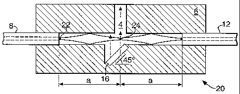
Referring to figure 2, an alternative VOA 20 according to the present
invention is
shown. In common with the device described with reference to figure 1, the VOA
20
comprises a T-shaped hollow core optical waveguide structure 4 formed in a
silicon
substrate 6 and having an input optical fibre 8 and an output optical fibre
12. A
MEMS moveable shutter 16 is also provided.
The VOA 20 does not however comprise ball lenses. The light from the input
optical
fibre 8 is coupled directly into the hollow core waveguide. The dimensions of
the T-
shaped hollow core optical waveguide structure 4 are arranged such that "re-
imaging" of the input beam injected into the hollow core waveguide from the
optical
fibre 8 occurs in the vicinity of the MEMS moveable shutter 16.
CA 02518069 2005-09-02
WO 2004/083915 PCT/GB2004/001075
14
The re-imaging phenomena is explained in more detail elsewhere; for example
see
PCT patent application GB2003/000331. In short, the hollow core optical
waveguide
structure to which the optical fibres are coupled may be formed so as to act
as a
multi-mode waveguide. Appropriately dimensioning the multi-mode waveguide
produces various beam splitting and combining functions in which beams can be
produced that are images of the input beam.
In particular, rectangular or square cross-section hollow multi-mode
waveguides can
be designed to provide re-imaging of symmetric, anti-symmetric or asymmetric
optical fields by designing the length of the waveguide to have an appropriate
relationship to its width and depth. In other words, the Gaussian input
profile of a
input beam is re-imaged (i.e. reproduced) after propagating a certain distance
along
a given waveguide. This effect also gives rise to beam replication; i.e.
multiple
images of the beam being formed a distances shorter than the re-imaging
length.
This effects is described previously in US5410625 and provides the basis for
multi-
mode interference (MMI) beam splitting devices.
As an example, a symmetric field in a square sectioned waveguide will have a
re-
imaging length is given by the square of the waveguide width over the
wavelength
of the propagating radiation. Re-imaging of the symmetric field occurs at the
re-
imaging length and multiples of the re-imaging length. Inbetween the re-
imaging
points, beam replication points and points of maximum field expansion are
found.
For the case of a 50.0 m wide hollow waveguide and 1.55 m radiation, the re-
imaging length is thus 1.613 mm. The symmetric field would be re-imaged at
this
length and also at integer multiples of this length, i.e. 3.23 mm, 4.84 mm
etc. For
example, a TEM00 Gaussian input beam from a single mode optical fibre could be
re-imaged at distances of 1.613 mm.
Alternatively, for the case of an asymmetric optical field, re-imaging occurs
at eight
times the length required for symmetric field re-imaging, - i.e. at 12.09 mm
for a
CA 02518069 2005-09-02
WO 2004/083915 PCT/GB2004/001075
50.0 m wide hollow waveguide. A mirror image of the asymmetric field is also
formed at half this length i.e. at 6.05 mm. In particular, offsetting the
input from the
centre line of the multimode region provides an asymmetric input that is re-
imaged
at pre-determined distances along the guide at an equivalent offset on either
side of
5 the centre line. Thus abeam could be re-imaged close to the edge of the
hollow core
guide, thereby minimising the travel of the shutter required to occlude the
beam.
In the case of a rectangular waveguide where the depth and width of the
waveguide
are substantially different, the re-imaging lengths associated with the two
10 waveguide cross-sectional dimensions (e.g. depth and width) are themselves
different. However, by arranging that the relationship between the dimensions
of the
rectangular hollow waveguide is such that re-imaging is produced at identical
lengths for the particular width and depth, any field can be re-imaged. Thus,
a
symmetric field can be re-imaged in a hollow rectangular waveguide by
arranging
15 that the re-imaging lengths associated with axes of width wl and w2 to be
identical.
The distance "a" in figure 2 represents the re-imaging distance for a Gaussian
light
beam injected into the hollow core optical waveguide from the input optical
fibre. It
can be seen that an image of the light beam 22 injected into the hollow core
optical
waveguide by the input fibre 8 is provided in the re-imaging region 24. The re-
imaged beam can thus be occluded by movement of the shutter 16 which is
located
in the vicinity of the re-imaging region 24. As the optical power of the beam
is
concentrated in the re-imaging region 24, the shutter movement required to
switch
between full and zero attenuation is reduced compared to that required in a
device of
the type described with reference to figure 1.
Referring to figure 3, the actuation mechanism 32 used to move the shutter 16
into,
and out of, the hollow core waveguide 4 of devices described with reference to
figures 1 and 2 is illustrated. The shutter 16 is held on an arm portion. 30
that is
coupled to a MEMS actuation mechanism 32 formed slightly away from the hollow
core waveguide structure 4.
CA 02518069 2005-09-02
WO 2004/083915 PCT/GB2004/001075
16
The MEMS actuation mechanism. 32 comprises an electro-thermal MEMS actuation
mechanism (e.g. a bent beam arrangement). Previously such mechanisms have been
disclosed that can provide large throw (e.g. 5-100 m full scale deflection)
actuation.
The shutter is in the plane of the wafer (i.e. vertical) and so may be
relatively low
footprint on the surface of the wafer.
Although electro-thermal actuation mechanisms are described, alternative
actuation
mechanisms, such electrostatic, electro-magnetic, bimorph, piezoelectric, etc,
may
be employed. In particular, an electro-static comb drive could be used to
provide the
desired movement. The shutter could be also formed as a "flip-up" structure;
this
would allow shutter shape to be more accurately defined. More detail on MEMS
device actuation technologies and the associated fabrication techniques can be
found
in "Fundamental of Microfabrication" by Marc Madou, published by CRC Press
(Boca Raton) in 1997; ISBN 0-8493-9451-1.
The final thickness of the shutter will depend on the degree of shutter
flatness
required and the device power handling capability. A low scalloping, highly
vertical
deep dry etch process is suitable for attaining such a structure. After
fabrication, the
shutter can be coated on both sides during a waveguide coating process to
provide
high reflectivity. As described above, the coating is typically a metal, but
dielectric
stacks and metal-dielectric stacks may also be used. It would be appreciated
by the
skilled person that active areas of electrostatic drives or electrothermal
drives may
require passivation or masking prior to the coating process to maintain
reliable
device operation.
The "waste light" reflected from the shutter 16 in VOA devices of the type
shown in
figures 1 and 2 can be transferred to a beam dump. This ensures the unwanted
light
does not increase noise or cause unwanted heating of a certain portion of the
substrate.
Referring to figure 4, a number of suitable hollow core beam dump arrangements
are
shown. Figure 4a shows a simple hollow core waveguide. end, figures 4b to 4c
show
CA 02518069 2005-09-02
WO 2004/083915 PCT/GB2004/001075
17
tapered hollow core waveguide beam dumps, figure 4d shows a spiral beam dump
whilst figures 4e to 4g show various circular beam dumps. The spiral and
circular
beams dump (which may also be tapered) provide the highest levels of beam
attenuation. The skilled person would select the exact design of taper for the
amount
of optical power which is to be dumped by the device. Although the hollow core
beam dumps can be used in VOAs, they can also be used in. any other device in
which optical power is to be dumped. In particular, such devices could form
part of
hollow core waveguide planar light circuits of the type described in PCT
patent
application GB2003/000331.
Referring to figure 5, a VOA 40 operable as a beam splitter or switch and
based on
the VOA described with reference to figure 1 is shown. Components of the VOA
40
similar to those described in figure 1 are assigned like reference numerals.
The VOA 40 comprises a T-shaped hollow core optical waveguide as described
with
reference to figure 1. However, any light reflected from the shutter 16 and
directed
along the third arm of the T-shaped hollow core waveguide is coupled into a
second
output optical fibre 42 via a second output ball lens 44.
In this manner, the VOA can operate as a beam splitting device or an optical
switch.
In other words, all or some of the light can be directed out of the optical
path
between the input fibre 8 and the output fibre 12 and to the second output
fibre 42.
Referring to figure 6, a further alternative VOA 60 based on the device
described
with reference to figure 1 is shown.
The VOA 60 comprises a cross shaped hollow core optical waveguide structure. A
first arm of the structure is linked to a first input optical fibre 62, a
second arm of the
structure is linked to a first output optical fibre 64, a third arm of the
structure is
linked to a second input optical fibre 66 and a fourth arm of the structure is
linked to
a second optical output fibre 68. Ball lenses 70, 72, 74 and 76 are provided
to
coupled light from the first, second, third and fourth arms to the first input
optical
CA 02518069 2005-09-02
WO 2004/083915 PCT/GB2004/001075
18
fibre 62, the first output optical fibre 64, the second input optical fibre 66
and the
second optical output fibre 68 respectively.
A reflective shutter 78 is insertable into the region of intersection of the
hollow core
optical waveguide arms. If the shutter 78 is fully retracted (i.e. fully
removed from
the hollow core optical waveguide) light from the first input optical fibre 62
passes
through the first and second arms of the device and exits via the first output
optical
fibre 64. Similarly, light from the second input optical fibre 66 passes
through the
third and fourth arms of the device and exits via the second output optical
fibre 68.
If the shutter 78 is fully inserted into the hollow waveguide structure, light
from the
first input optical fibre 62 passes through the first and fourth arms of the
device and
exits via the second output optical fibre 68. Light from the second input
optical fibre
66 passes through the third and second arms of the device and exits via the
first
output optical fibre 64. In other words, full insertion of the shutter swaps
the output
fibre through which light from a given input exits the device. Partial
insertion of the
shutter 78 allows light from each input to be split between the two outputs
(i.e. the
device can operate as a two way analogue switch.