Note: Descriptions are shown in the official language in which they were submitted.
CA 02518805 2005-09-12
Internal reference: IR~M.053 NON-EP / IOC-040016U1
METHOD AND SYSTEM FOR PACKAGING A DISPLAY
Background
Field
The field of the invention relates to microelectromechanical systems (MEMS)
and the
packaging of such systems. More specifically, the field of the invention
relates to interferometric
modulators and methods of fabricating such modulators under ambient
conditions.
Description of the Related TechnoloQy
Microelectromechanical systems (MEMS) include micro mechanical elements,
actuators,
and electronics. Micromechanical elements may be created using deposition,
etching, and or
other micromachining processes that etch away parts of substrates and/or
deposited material
layers or that add layers to form electrical and electromechanical devices.
One type of MEMS
device is called an interferometric modulator. As used herein, the term
interferometric modulator
or interferometric light modulator refers to a device that selectively absorbs
and/or reflects light
using the principles of optical interference. In certain embodiments, an
interferometric modulator
may comprise a pair of conductive plates, one or both of which may be
transparent and/or
reflective in whole or part and capable of relative motion upon application of
an appropriate
electrical signal. In a particular embodiment, one plate may comprise a
stationary layer
deposited on a substrate and the other plate may comprise a metallic membrane
separated from
the stationary layer by an air gap. As described herein in more detail, the
position of one plate in
relation to another can change the optical interference of light incident on
the interferometric
modulator. Such devices have a wide range of applications, and it would be
beneficial in the art
to utilize and/or modify the characteristics of these types of devices so that
their features can be
exploited in improving existing products and creating new products that have
not yet been
developed.
Summary of Certain Embodiments
The system, method, and devices of the invention each have several aspects, no
single
one of which is solely responsible for its desirable attributes. Without
limiting the scope of this
invention, its more prominent features will now be discussed briefly. After
considering this
discussion, and particularly after reading the section entitled "Detailed
Description of Certain
Embodiments" one will understand how the features of this invention provide
advantages over
-1-
CA 02518805 2005-09-12
other display devices. The embodiments described herein provide a package
structure and a
method of manufacturing a package structure in ambient conditions.
One embodiment of the invention is a method of manufacturing a display device,
comprising: providing a transparent substrate having an interferometric
modulator formed
thereon; and joining a backplane to the transparent substrate to form a
package by applying a seal
between the backplane and the transparent substrate, wherein the
interferometric modulator is
encapsulated by the package and the package has at least one opening.
Another embodiment of the invention is a display device made by the method of
providing a transparent substrate having an interferometric modulator formed
thereon; and
joining a backplane to the transparent substrate to form a package by applying
a seal between the
backplane and the transparent substrate, wherein the interferometric modulator
is encapsulated by
the package and the package has at least one opening.
Yet another embodiment is a microelectromechanical systems based device,
comprising:
transmissive means for transmitting light therethrough; modulating means for
modulating light
transmitted through said transmissive means; covering means for covering said
modulating
means; and sealing means for joining the covering means to the transmissive
means to form a
package, and wherein either the covering means or the sealing means comprises
a sealed opening.
Still another embodiment is a microelectromechanical systems based device,
comprising:
a transparent substrate having a microelectromechanical device formed thereon;
a backplane; and
a seal configured to join the backplane to the transparent substrate to
encapsulate the
microelectromechanical device within a package, wherein either the backplane
or seal has a
sealed opening.
One other embodiment is a method of manufacturing a display device,
comprising:
providing a transparent substrate having a microelectromechanical device
formed thereon;
joining a backplane to the transparent substrate to form a package by applying
a seal between the
backplane and the transparent substrate, wherein the microelectromechanical
device is
encapsulated by the package and the package has at least one opening; and
reducing water
content in the package by introducing a gas through the at least one opening
and into the package.
An additional embodiment is a display device made by the method of providing a
transparent substrate having a microelectromechanical device formed thereon;
joining a
backplane to the transparent substrate to form a package by applying a seal
between the
backplane and the transparent substrate, wherein the microelectromechanical
device is
encapsulated by the package and the package has at least one opening; and
reducing water
content in the package by introducing a gas through the at least one opening
and into the package.
Another embodiment is a display device, comprising: transmissive means for
transmitting
light therethrough; modulating means for modulating light transmitted through
said transmissive
-2-
CA 02518805 2005-09-12
means; covering means for covering said modulating means; and sealing means
for joining the
backplane to the transparent substrate to encapsulate the
microelectromechanical device within a
package, wherein the package has at least one endseal, and wherein to remove
moisture content
within the package, the at least one endseal is configured to allow gas to
flow therethrough prior
to the at least one endseal being sealed.
An additional embodiment is a microelectromechanical systems based device,
comprising: a transparent substrate having a microelectromechanical device
formed thereon; a
backplane; and a seal joining the backplane to the transparent substrate to
encapsulate the
microelectromechanical device within a package, wherein the seal is applied
between the
backplane and the transparent substrate and the package has at least one
endseal, wherein, to
remove moisture content within the package, the at least one endseal is
configured to allow gas to
flow therethrough prior to the at least one endseal being sealed.
Brief Description of the Drawings
I S These and other aspects of the invention will be readily apparent from the
following
description and from the appended drawings (not to scale), which are meant to
illustrate and not
to limit the invention, and wherein:
Figure 1 is an isometric view depicting a portion of one embodiment of an
interferometric modulator display in which a movable reflective layer of a
first interferometric
modulator is in a released position and a movable reflective layer of a second
interferometric
modulator is in an actuated position.
Figure 2 is a system block diagram illustrating one embodiment of an
electronic device
incorporating a 3x3 interferometric modulator display.
Figure 3 is a diagram of movable minor position versus applied voltage for one
exemplary embodiment of an interferometric modulator of Figure 1.
Figure 4 is an illustration of a set of row and column voltages that may be
used to drive
an interferometric modulator display.
Figure SA illustrates one exemplary frame of display data in the 3x3
interferometric
modulator display of Figure 2.
Figure SB illustrates one exemplary timing diagram for row and column signals
that may
be used to write the frame of Figure SA.
Figures 6A and 6B are system block diagrams illustrating an embodiment of a
display
device.
Figure 7A is a cross section of the device of Figure 1.
Figure 7B is a cross section of an alternative embodiment of an
interferometric
modulator.
-3-
CA 02518805 2005-09-12
Figure 7C is a cross section of another alternative embodiment of an
interferometric
modulator.
Figure 8 is a cross-section of a basic package structure.
Figure 9A is a cross-section of a package structure in accordance with an
embodiment
having an opening in the backplane.
Figure 9B is a cross-section of a package structure in accordance with an
embodiment
having an opening in the perimeter seal.
Figure 9C is a top plan view of a package structure shown in Figure 9B.
Figure 9D is a top plan view of a backplane having openings according to an
embodiment.
Figure 9E is a cross-sectional view of a package structure having openings in
the
backplane.
Figure 9F is a top plan view of a backplane having openings according to
another
embodiment.
Figure 9G is a top plan view of a backplane having openings according to yet
another
embodiment.
Figure 10 is a cross-section of a package structure in accordance with an
embodiment
having an opening in the backplane and desiccant within the package.
Figures 11 A-11 B are schematic views showing a process of removing water
vapor from
the package according to an embodiment.
Figure 11 C is a top plan view of the embodiment shown in Figure 11B.
Figure 12 is a schematic view showing a process of removing water vapor from
the
package according to another embodiment.
Figure 13 is a schematic view showing a process of removing water vapor from
the
package according to still embodiment.
Figure 14 is a schematic view showing a process of removing water vapor from
the
package according to yet another embodiment.
Figure I S is a schematic view showing a process of removing water vapor from
the
package according to yet another embodiment.
Figures 16A-16C are a schematic view showing a process of removing water vapor
from
the package according to yet another embodiment.
Figure 17A is a schematic view showing a process of sealing openings according
to an
embodiment.
Figure 17B is a top plan view of the embodiment shown in Figure 17A prior to
sealing
the openings.
CA 02518805 2005-09-12
Figures 18A and 18B are system block diagrams illustrating an embodiment of a
visual
display device comprising a plurality of interferometric modulators.
Detailed Description of Certain Embodiments
The following detailed description is directed to certain specific embodiments
of the
invention. However, the invention can be embodied in a multitude of different
ways. In this
description, reference is made to the drawings wherein like parts are
designated with like
numerals throughout. As will be apparent from the following description, the
embodiments may
be implemented in any device that is configured to display an image, whether
in motion (e.g.,
video) or stationary (e.g., still image), and whether textual or pictorial.
More particularly, it is
contemplated that the embodiments may be implemented in or associated with a
variety of
electronic devices such as, but not limited to, mobile telephones, wireless
devices, personal data
assistants (PDAs), hand-held or portable computers, GPS receivers/navigators,
cameras, MP3
players, camcorders, game consoles, wrist watches, clocks, calculators,
television monitors, flat
panel displays, computer monitors, auto displays (e.g., odometer display,
etc.), cockpit controls
and/or displays, display of camera views (e.g., display of a rear view camera
in a vehicle),
electronic photographs, electronic billboards or signs, projectors,
architectural structures,
packaging, and aesthetic structures (e.g., display of images on a piece of
jewelry). MEMS
devices of similar structure to those described herein can also be used in non-
display applications
such as in electronic switching devices.
One interferometric modulator display embodiment comprising an interferometric
MEMS display element is illustrated in Figure 1. In these devices, the pixels
are in either a
bright or dark state. In the bright ("on" or "open") state, the display
element reflects a large
portion of incident visible light to a user. When in the dark ("off ' or
"closed") state, the display
element reflects little incident visible light to the user. Depending on the
embodiment, the light
reflectance properties of the "on" and "off ' states may be reversed. MEMS
pixels can be
configured to reflect predominantly at selected colors, allowing for a color
display in addition to
black and white.
Figure 1 is an isometric view depicting two adjacent pixels in a series of
pixels of a
visual display, wherein each pixel comprises a MEMS interferometric modulator.
In some
embodiments, an interferometric modulator display comprises a row/column array
of these
interferometric modulators. Each interferometric modulator includes a pair of
reflective layers
positioned at a variable and controllable distance from each other to form a
resonant optical
cavity with at least one variable dimension. In one embodiment, one of the
reflective layers may
be moved between two positions. In the first position, referred to herein as
the relaxed, the
movable layer is positioned at a relatively large distance from a fixed
partially reflective layer. In
-5-
CA 02518805 2005-09-12
the second position, the movable layer is positioned more closely adjacent to
the partially
reflective layer. Incident light that reflects from the two layers interferes
constructively or
destructively depending on the position of the movable reflective layer,
producing either an
overall reflective or non-reflective state for each pixel.
The depicted portion of the pixel array in Figure 1 includes two adjacent
interferometric
modulators 12a and 12b. In the interferometric modulator 12a on the left, a
movable and highly
reflective layer 14a is illustrated in a relaxed position at a predetermined
distance from a fixed
partially reflective layer 16a. In the interferometric modulator 12b on the
right, the movable
highly reflective layer 14b is illustrated in an actuated position adjacent to
the fixed partially
reflective layer 16b.
The fixed layers 16a, 16b are electrically conductive, partially transparent
and partially
reflective, and may be fabricated, for example, by depositing one or more
layers each of
chromium and indium-tin-oxide onto a transparent substrate 20. The layers are
patterned into
parallel strips, and may form row electrodes in a display device as described
further below. The
movable layers 14a, 14b may be formed as a series of parallel strips of a
deposited metal layer or
layers (orthogonal to the row electrodes 16a, 16b) deposited on top of posts
18 and an intervening
sacrificial material deposited between the posts 18. When the sacrificial
material is etched away,
the deformable metal layers 14a, 14b are separated from the fixed metal layers
by a defined gap
19. A highly conductive and reflective material such as aluminum may be used
for the
deformable layers, and these strips may form column electrodes in a display
device.
With no applied voltage, the cavity 19 remains between the layers 14a, 16a and
the
deformable layer is in a mechanically relaxed state as illustrated by the
pixel 12a in Figure 1.
However, when a potential difference is applied to a selected row and column,
the capacitor
formed at the intersection of the row and column electrodes at the
corresponding pixel becomes
charged, and electrostatic forces pull the electrodes together. If the voltage
is high enough, the
movable layer is deformed and is forced against the fixed layer (a dielectric
material which is not
illustrated in this Figure may be deposited on the fixed layer to prevent
shorting and control the
separation distance) as illustrated by the pixel 12b on the right in Figure 1.
The behavior is the
same regardless of the polarity of the applied potential difference. In this
way, row/column
actuation that can control the reflective vs. non-reflective pixel states is
analogous in many ways
to that used in conventional LCD and other display technologies.
Figures 2 through SB illustrate one exemplary process and system for using an
array of
interferometric modulators in a display application.
Figure 2 is a system block diagram illustrating one embodiment of an
electronic device
that may incorporate aspects of the invention. In the exemplary embodiment,
the electronic
device includes a processor 21 which may be any general purpose single- or
mufti-chip
-6-
CA 02518805 2005-09-12
microprocessor such as an ARM, Pentium~, Pentium II~, Pentium III~, Pentium
IV~,
Pentium~ Pro, an 8051, a MIPS~, a Power PCB, an ALPHA~, or any special purpose
microprocessor such as a digital signal processor, microcontroller, or a
programmable gate array.
As is conventional in the art, the processor 21 may be configured to execute
one or more software
modules. In addition to executing an operating system, the processor may be
configured to
execute one or more software applications, including a web browser, a
telephone application, an
email program, or any other software application.
In one embodiment, the processor 21 is also configured to communicate with an
array
controller 22. In one embodiment, the array controller 22 includes a row
driver circuit 24 and a
column driver circuit 26 that provide signals to a display array or panel 30.
The cross section of
the array illustrated in Figure 1 is shown by the lines 1-1 in Figure 2. For
MEMS interferometric
modulators, the row/column actuation protocol may take advantage of a
hysteresis property of
these devices illustrated in Figure 3. It may require, for example, a 10 volt
potential difference to
cause a movable layer to deform from the relaxed state to the actuated state.
However, when the
voltage is reduced from that value, the movable layer maintains its state as
the voltage drops back
below 10 volts. In the exemplary embodiment of Figure 3, the movable layer
does not relax
completely until the voltage drops below 2 volts. There is thus a range of
voltage, about 3 to 7 V
in the example illustrated in Figure 3, where there exists a window of applied
voltage within
which the device is stable in either the relaxed or actuated state. This is
referred to herein as the
"hysteresis window" or "stability window." For a display array having the
hysteresis
characteristics of Figure 3, the row/column actuation protocol can be designed
such that during
row strobing, pixels in the strobed row that are to be actuated are exposed to
a voltage difference
of about 10 volts, and pixels that are to be relaxed are exposed to a voltage
difference of close to
zero volts. After the strobe, the pixels are exposed to a steady state voltage
difference of about S
volts such that they remain in whatever state the row strobe put them in.
After being written,
each pixel sees a potential difference within the "stability window" of 3-7
volts in this example.
This feature makes the pixel design illustrated in Figure 1 stable under the
same applied voltage
conditions in either an actuated or relaxed pre-existing state. Since each
pixel of the
interferometric modulator, whether in the actuated or relaxed state, is
essentially a capacitor
formed by the fixed and moving reflective layers, this stable state can be
held at a voltage within
the hysteresis window with almost no power dissipation. Essentially no current
flows into the
pixel if the applied potential is fixed.
In typical applications, a display frame may be created by asserting the set
of column
electrodes in accordance with the desired set of actuated pixels in the first
row. A row pulse is
then applied to the row 1 electrode, actuating the pixels corresponding to the
asserted column
lines. The asserted set of column electrodes is then changed to correspond to
the desired set of
CA 02518805 2005-09-12
actuated pixels in the second row. A pulse is then applied to the row 2
electrode, actuating the
appropriate pixels in row 2 in accordance with the asserted column electrodes.
The row 1 pixels
are unaffected by the row 2 pulse, and remain in the state they were set to
during the row 1 pulse.
This may be repeated for the entire series of rows in a sequential fashion to
produce the frame.
Generally, the frames are refreshed and/or updated with new display data by
continually
repeating this process at some desired number of frames per second. A wide
variety of protocols
for driving row and column electrodes of pixel arrays to produce display
frames are also well
known and may be used in conjunction with the present invention.
Figures 4, SA, and SB illustrate one possible actuation protocol for creating
a display
frame on the 3x3 array of Figure 2. Figure 4 illustrates a possible set of
column and row voltage
levels that may be used for pixels exhibiting the hysteresis curves of Figure
3. In the Figure 4
embodiment, actuating a pixel involves setting the appropriate column to -
Vbias, and the
appropriate row to +0V, which may correspond to -5 volts and +5 volts
respectively Relaxing
the pixel is accomplished by setting the appropriate column to +Vbias, and the
appropriate row to
the same +0V, producing a zero volt potential difference across the pixel. In
those rows where
the row voltage is held at zero volts, the pixels are stable in whatever state
they were originally
in, regardless of whether the column is at +Vbias, or -Vbias. As is also
illustrated in Figure 4, it
will be appreciated that voltages of opposite polarity than those described
above can be used,
e.g., actuating a pixel can involve setting the appropriate column to +Vbias,
and the appropriate
row to -0V. In this embodiment, releasing the pixel is accomplished by setting
the appropriate
column to -Vbias, and the appropriate row to the same -OV, producing a zero
volt potential
difference across the pixel.
Figure SB is a timing diagram showing a series of row and column signals
applied to the
3x3 array of Figure 2 which will result in the display arrangement illustrated
in Figure SA, where
actuated pixels are non-reflective. Prior to writing the frame illustrated in
Figure SA, the pixels
can be in any state, and in this example, all the rows are at 0 volts, and all
the columns are at +5
volts. With these applied voltages, all pixels are stable in their existing
actuated or relaxed states.
In the Figure SA frame, pixels (1,1), (1,2), (2,2), (3,2) and (3,3) are
actuated. To
accomplish this, during a "line time" for row 1, columns I and 2 are set to -5
volts, and column 3
is set to +5 volts. This does not change the state of any pixels, because all
the pixels remain in
the 3-7 volt stability window. Row 1 is then strobed with a pulse that goes
from 0, up to 5 volts,
and back to zero. This actuates the (1,1) and (1,2) pixels and relaxes the
(1,3) pixel. No other
pixels in the array are affected. To set row 2 as desired, column 2 is set to -
5 volts, and columns
1 and 3 are set to +5 volts. The same strobe applied to row 2 will then
actuate pixel (2,2) and
relax pixels (2,1) and (2,3). Again, no other pixels of the array are
affected. Row 3 is similarly
set by setting columns 2 and 3 to -5 volts, and column 1 to +5 volts. The row
3 strobe sets the
_g_
CA 02518805 2005-09-12
row 3 pixels as shown in Figure SA. After writing the frame, the row
potentials are zero, and the
column potentials can remain at either +5 or -5 volts, and the display is then
stable in the
arrangement of Figure SA. It will be appreciated that the same procedure can
be employed for
arrays of dozens or hundreds of rows and columns. It will also be appreciated
that the timing,
sequence, and levels of voltages used to perform row and column actuation can
be varied widely
within the general principles outlined above, and the above example is
exemplary only, and any
actuation voltage method can be used with the systems and methods described
herein.
Figures 6A and 6B are system block diagrams illustrating an embodiment of a
display
device 40. The display device 40 can be, for example, a cellular or mobile
telephone. However,
the same components of display device 40 or slight variations thereof are also
illustrative of
various types of display devices such as televisions and portable media
players.
The display device 40 includes a housing 41, a display 30, an antenna 43, a
speaker 44,
an input device 48, and a microphone 46. The housing 41 is generally formed
from any of a
variety of manufacturing processes as are well known to those of skill in the
art, including
injection molding, and vacuum forming. In addition, the housing 41 may be made
from any of a
variety of materials, including but not limited to plastic, metal, glass,
rubber, and ceramic, or a
combination thereof. In one embodiment the housing 41 includes removable
portions (not
shown) that may be interchanged with other removable portions of different
color, or containing
different logos, pictures, or symbols.
The display 30 of exemplary display device 40 may be any of a variety of
displays,
including a bi-stable display, as described herein. In other embodiments, the
display 30 includes a
flat-panel display, such as plasma, EL, OLED, STN LCD, or TFT LCD as described
above, or a
non-flat-panel display, such as a CRT or other tube device, as is well known
to those of skill in
the art. However, for purposes of describing the present embodiment, the
display 30 includes an
interferometric modulator display, as described herein.
The components of one embodiment of exemplary display device 40 are
schematically
illustrated in Figure 6B. The illustrated exemplary display device 40 includes
a housing 41 and
can include additional components at least partially enclosed therein. For
example, in one
embodiment, the exemplary display device 40 includes a network interface 27
that includes an
antenna 43 which is coupled to a transceiver 47. The transceiver 47 is
connected to a processor
21, which is connected to conditioning hardware 52. The conditioning hardware
52 may be
confgured to condition a signal (e.g. filter a signal). The conditioning
hardware 52 is connected
to a speaker 44 and a microphone 46. The processor 21 is also connected to an
input device 48
and a driver controller 29. The driver controller 29 is coupled to a frame
buffer 28, and to an
array driver 22, which in turn is coupled to a display array 30. A power
supply 50 provides
power to all components as required by the particular exemplary display device
40 design.
-9-
CA 02518805 2005-09-12
The network interface 27 includes the antenna 43 and the transceiver 47 so
that the
exemplary display device 40 can communicate with one ore more devices over a
network. In one
embodiment the network interface 27 may also have some processing capabilities
to relieve
requirements of the processor 21. The antenna 43 is any antenna known to those
of skill in the
art for transmitting and receiving signals. In one embodiment, the antenna
transmits and receives
RF signals according to the IEEE 802.11 standard, including IEEE 802.11(a),
(b), or (g). In
another embodiment, the antenna transmits and receives RF signals according to
the
BLUETOOTH standard. In the case of a cellular telephone, the antenna is
designed to receive
CDMA, GSM, AMPS or other known signals that are used to communicate within a
wireless cell
phone network. The transceiver 47 pre-processes the signals received from the
antenna 43 so that
they may be received by and further manipulated by the processor 21. The
transceiver 47 also
processes signals received from the processor 21 so that they may be
transmitted from the
exemplary display device 40 via the antenna 43.
In an alternative embodiment, the transceiver 47 can be replaced by a
receiver. In yet
another alternative embodiment, network interface 27 can be replaced by an
image source, which
can store or generate image data to be sent to the processor 21. For example,
the image source
can be a digital video disc (DVD) or a hard-disc drive that contains image
data, or a software
module that generates image data.
Processor 21 generally controls the overall operation of the exemplary display
device 40.
The processor 21 receives data, such as compressed image data from the network
interface 27 or
an image source, and processes the data into raw image data or into a format
that is readily
processed into raw image data. The processor 21 then sends the processed data
to the driver
controller 29 or to frame buffer 28 for storage. Raw data typically refers to
the information that
identifies the image characteristics at each location within an image. Far
example, such image
characteristics can include color, saturation, and gray-scale level.
In one embodiment, the processor 21 includes a microcontroller, CPU, or logic
unit to
control operation of the exemplary display device 40. Conditioning hardware 52
generally
includes amplifiers and filters for transmitting signals to the speaker 44,
and for receiving signals
from the microphone 46. Conditioning hardware 52 may be discrete components
within the
exemplary display device 40, or may be incorporated within the processor 21 or
other
components.
The driver controller 29 takes the raw image data generated by the processor
21 either
directly from the processor 21 or from the frame buffer 28 and reformats the
raw image data
appropriately for high speed transmission to the array driver 22.
Specifically, the driver
controller 29 reformats the raw image data into a data flow having a raster-
like format, such that
it has a time order suitable for scanning across the display array 30. Then
the driver controller 29
-10-
CA 02518805 2005-09-12
sends the formatted information to the array driver 22. Although a driver
controller 29, such as a
LCD controller, is often associated with the system processor 21 as a stand-
alone Integrated
Circuit (IC), such controllers may be implemented in many ways. They may be
embedded in the
processor 21 as hardware, embedded in the processor 21 as software, or fully
integrated in
hardware with the array driver 22.
Typically, the array driver 22 receives the formatted information from the
driver
controller 29 and reformats the video data into a parallel set of waveforms
that are applied many
times per second to the hundreds and sometimes thousands of leads coming from
the display's x-
y matrix of pixels.
In one embodiment, the driver controller 29, array driver 22, and display
array 30 are
appropriate for any of the types of displays described herein. For example, in
one embodiment,
driver controller 29 is a conventional display controller or a bi-stable
display controller (e.g., an
interferometric modulator controller). In another embodiment, array driver 22
is a conventional
driver or a bi-stable display driver (e.g., an interferometric modulator
display). In one
embodiment, a driver controller 29 is integrated with the array driver 22.
Such an embodiment is
common in highly integrated systems such as cellular phones, watches, and
other small area
displays. In yet another embodiment, display array 30 is a typical display
array or a bi-stable
display array (e.g., a display including an array of interferometric
modulators).
The input device 48 allows a user to control the operation of the exemplary
display
device 40. In one embodiment, input device 48 includes a keypad, such as a
QWERTY keyboard
or a telephone keypad, a button, a switch, a touch-sensitive screen, a
pressure- or heat-sensitive
membrane. In one embodiment, the microphone 46 is an input device for the
exemplary display
device 40. When the microphone 46 is used to input data to the device, voice
commands may be
provided by a user for controlling operations of the exemplary display device
40.
Power supply 50 can include a variety of energy storage devices as are well
known in the
art. For example, in one embodiment, power supply 50 is a rechargeable
battery, such as a
nickel-cadmium battery or a lithium ion battery. In another embodiment, power
supply 50 is a
renewable energy source, a capacitor, or a solar cell, including a plastic
solar cell, and solar-cell
paint. In another embodiment, power supply 50 is configured to receive power
from a wall
outlet.
In some implementations control programmability resides, as described above,
in a driver
controller which can be located in several places in the electronic display
system. In some cases
control programmability resides in the array driver 22. Those of skill in the
art will recognize
that the above-described optimization may be implemented in any number of
hardware and/or
software components and in various configurations.
-11-
CA 02518805 2005-09-12
The details of the structure of interferometric modulators that operate in
accordance with
the principles set forth above may vary widely. For example, Figures 7A-7C
illustrate three
different embodiments of the moving mirror structure. Figure 7A is a cross
section of the
embodiment of Figure 1, where a strip of metal material 14 is deposited on
orthogonally
extending supports 18. In Figure 7B, the moveable reflective material 14 is
attached to supports
at the corners only, on tethers 32. In Figure 7C, the moveable reflective
material 14 is suspended
from a deformable layer 34. This embodiment has benefits because the
structural design and
materials used for the reflective material 14 can be optimized with respect to
the optical
properties, and the structural design and materials used for the deformable
layer 34 can be
optimized with respect to desired mechanical properties. The production of
various types of
interferometric devices is described in a variety of published documents,
including, for example,
U.S. Published Application 2004/0051929. A wide variety of known techniques
may be used to
produce the above described structures involving a series of material
deposition, patterning, and
etching steps.
Packaging techniques for interferometric modulators will be described in more
detail
below. Interferometric modulators typically include moving parts, such as the
movable mirrors
14a, 14b that must have a protected space in which to move. A schematic of a
basic package
structure 700 for an interferometric modulator is illustrated in Figure 8. As
shown in Figure 8, a
basic package structure 700 includes a transparent substrate 710 and a
backplane cover or "cap"
720. As illustrated in Figure 8, an interferometric modulator 730 is
encapsulated within the
package structure 700. Preferably, the backplane 720 and transparent substrate
710 are sealed
together to protect the interferometric modulator 730 from harmful elements in
the environment.
A method of packaging an interferometric modulator according to the embodiment
shown
in Figure 8 will be discussed in more detail below. The packages and packaging
methods
described herein may be used for packaging any interferometric modulator,
including, but not
limited to, the interferometric modulators described above.
As discussed above, the interferometric modulator 730 is conftgured to reflect
light
through the transparent substrate and includes moving parts, such as the
movable mirrors 14a,
14b. Therefore, to allow such moving parts to move, a gap or cavity 770 is
preferably created
between such moving parts and the backplane 720. The gap or cavity 770 allows
the mechanical
parts, such as the movable mirrors 14a, 14b, of the interferometric modulator
730 to move. It will
be understood that, in an embodiment, the gap or cavity 770 is created when a
backplane 720
having a recessed area is joined to the transparent substrate 710, as shown in
Figure 8.
The transparent substrate 710 may be any transparent substance capable of
having thin
film, MEMS devices built upon it. Such transparent substances include, but are
not limited to,
-12-
CA 02518805 2005-09-12
glass, plastic, and transparent polymers. Images are displayed through the
transparent substrate
710, which serves as an imaging surface.
In accordance with an embodiment, an interferometric modulator 730 is
preferably
formed on a transparent substrate 710. It will be understood that the fixed
mirrors 16a, 16b of the
interferometric modulator 730 are adjacent the transparent substrate 710 and
the movable mirrors
14a, 14b are formed over the fixed mirrors 16a, 16b such that the movable
mirrors 14a, 14b may
move within the cavity 770 of the package structure 700 of the embodiment
shown in Figure 8.
To form the interferometric modulator 730, the transparent substrate 710, in
one
embodiment, is covered with indium tin oxide (ITO). The ITO may be deposited
by standard
deposition techniques, including chemical vapor deposition (CVD) and
sputtering, preferably to a
thickness of about 500 t~. A relatively thin layer of chrome is preferably
deposited over the ITO.
The ITO/chrome bilayer is then etched and patterned into columns to form the
column electrodes
16a, 16b. A layer of silicon dioxide (Si02) is preferably formed over the
ITO/chrome columns to
create partially reflective fixed mirrors 16a, 16b. A sacrificial layer of
silicon (Si) is preferably
deposited (and later released) over the structure to create a resonant optical
cavity between the
fixed mirrors 16a, 16b and the movable mirrors 14a, 14b. In other embodiments,
this sacrificial
layer may be formed of molybdenum (Mo), tungsten (~, or titanium (Ti).
Another mirror layer, preferably formed of aluminum, is deposited over the
sacrificial
Iayer of silicon to form the movable mirrors 14a, 14b of the interferometric
modulator 730. This
mirror layer is deposited and patterned into rows orthogonal to the column
electrodes 16a, 16b to
create the row/column array described above. In other embodiments, this mirror
layer may
comprise highly reflective metals, such as, for example, silver (Ag) or gold
(Au). Alternatively,
this minor layer may be a stack of metals configured to give the proper
optical and mechanical
properties.
The sacrificial layer of silicon is removed, preferably using a gas etching
process, after
the movable mirrors 14a, 14b are formed to create the optical cavity between
the fixed mirrors
16a, 16b and the movable mirrors 14a, 14b. In an embodiment, this sacrificial
layer is removed
a8er the backplane is joined to the transparent substrate through an opening
in either the
backplane or perimeter seal, as will be described in more detail below.
Standard etching
techniques may be used to remove the sacrificial layer of silicon. The
particular release etching
will depend on the material to be released. For example, xenon diflouride
(XeF2) may be used to
remove the silicon sacrificial layer. In another embodiment, the sacrificial
layer of silicon
between the mirrors 16a, 16b, 14a, 14b is removed before the backplane 720 is
joined to the
transparent substrate 710. The skilled artisan will appreciate that each layer
of the
interferometric modulator 730 is preferably deposited and patterned using
standard deposition
techniques and standard photolithographic techniques.
-13-
CA 02518805 2005-09-12
The skilled artisan will understand that the backplane 720 serves a mechanical
function,
protecting the interferometric modulator 730 from contaminants in the
environment. The
backplane 720 along with the transparent substrate 710 and a seal 740 (which
is described in
more detail below) prevent mechanical interference, moisture, and contaminant
gases from
reaching and potentially damaging the interferometric modulator 730 within the
package 700.
The backplane 720 may therefore be formed of any suitable material, whether
transparent or
opaque, conductive or insulating. Suitable materials for the backplane 720
include, but are not
limited to, glass (e.g., float, 1737, soda lime), plastic, ceramics, polymers,
laminates, and metals
and metal foils (e.g., stainless steel (SS302, SS410), Kovar, plated Kovar).
A sealing means or a seal 740 is typically provided to join the transparent
substrate 710
and the backplane 720 to form the package structure 700. The seal 740 is
typically a semi-
hermetic seal, such as a conventional epoxy-based adhesive. In other
embodiments, the seal 740
may be Polyisobutylene (PIB), o-rings, polyurethane, thin film metal weld,
liquid spin-on glass,
solders, polymers, or plastics, among other types of seals. In still other
embodiment, the seal 740
may be a hermetic seal.
Once the backplane 720 and transparent substrate 710 are joined, the seal 740
may be
cured and hardened. The skilled artisan will appreciate that the seal 740,
which may be
hardened, between the backplane 720 and the transparent substrate 710 is
different from seals
that may be applied after division of the package structure 700 into
individual arrays.
It is generally desirable to manufacture several arrays of interferometric
modulators on a
single transparent substrate, apply the backplane, and then divide the
structure into individual
arrays. Once the seal 740 is hardened, the structure may be mechanically or
laser scribed or
otherwise prepared for division. Depending on the seal 740, as well as other
factors, it may be
necessary, after the division, to apply an endseal to the individual package
structures or arrays.
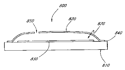
A side-view illustration of an embodiment of a package structure 800 having an
endseal
opening is shown in Figure 9A. An endseal opening is typically either an
opening in an
otherwise continuous perimeter seal (as shown in Figure 9B) or an opening or
hole 850 in the
backplane 820, as shown in Figure 9A. Figure 9C is a top plan view of the
embodiment shown in
Figure 9B. As shown in Figures 9B and 9C, the perimeter seal is not
continuously dispensed,
leaving an opening 860 in the seal 840.
It will be understood that there may be more than one opening 850 in the
backplane, as
shown in Figures 9D-9G. In the embodiment shown in Figure 9A, the opening or
hole 850 may
be closed to form an endseal or sealed opening to complete the package 800
with, for example, a
metal or glass cap, metal foil, adhesive, solder, or W or thermally cured
polymer.
It is appreciated that there are other uses for metal caps. For example, metal
caps may be
used with a backplane formed of a printed circuit board (PCB) backplane that
may include
-14-
CA 02518805 2005-09-12
electronic interfaces for use with radio-frequency (RF) signals. A PCB
backplane may serve not
only as protection for circuitry that is integrated into the backplane but may
also enhance RF
circuit needs. For example, metal caps may be included for RF enhancement or
protection.
Antenna properties may also be incorporated into the PCB backplane or the
interferometric
modulator, including, but not limited to, the use of a metal backplane or a
metal cap as an antenna
for a cellular phone.
The use of such openings or holes 850 in the packaging process allows
packaging to take
place in ambient conditions, outside of a pressure controlled chamber.
Generally ambient
conditions are the laboratory conditions in a particle-free clean room
typically having a
temperature around 70°F and relative humidity in the range of about 40-
60%, and more
preferably about 50%. The openings or holes 850 allow pressure within the
package 800 to
escape so that the pressure does not cause the transparent substrate 810 and
the backplane 820 to
come apart during the joining or sealing process because pressure does not
build up within the
package 800. Allowing the pressure within the package to escape via the
openings 850 provides
for constant pressure within the package 850, which also allows a more uniform
seal width even
if the seal is not dispensed with a uniform thickness.
The opening or hole 850 may also be configured to allow material to enter and
exit the
package 800. In particular, the opening or hole 850 may be configured to allow
for application of
a solvent to the interferometric modulator 830 for removal of a spacer or
sacrificial layer, which
will be described in more detail below. The skilled artisan will understand
that an endseal may
not be necessary, as will be described in more detail below.
Generally, it is desirable to minimize the permeation of water vapor into the
package
structure 800 and thus control the environment inside the package structure
800. The package
structure 800 may be hermetically sealed to ensure the environment within the
package structure
800 remains constant regardless of the surrounding environment. An example of
a hermetic
sealing process is disclosed in U.S. Patent No. 6,589,625, the entirety of
which is hereby
incorporated by reference.
In one embodiment having a hermetic seal, the seal 840 is a hermetic barrier
that acts as
an environmental barrier preventing all air and water vapor from flowing
through the seal 840
and entering the package structure 800. Suitable materials for a hermetic seal
include, but are not
limited to, welds, solders, adhesives mixed with molecular sieves, such as a
zeolite. The
adhesive component alone cannot act as a suitable environmental barrier
because it will
eventually allow moisture and other contaminants to permeate into the package
structure 800. A
semi-hermetic seal 840 of one of the aforementioned materials is desirable for
space-critical
environments because the seal 840 can be very thin and inexpensive, relative
to other sealing
techniques, such as welding and soldering. The semi-hermetic seal 840 may be
applied through
-15-
CA 02518805 2005-09-12
simple in-line manufacturing processes, whereas the techniques of welding and
soldering for
hermetic seals require very high temperature processes that can damage the
package structure
800, are relatively expensive, and tend to occupy much more space because a
welded or soldered
seal is thicker. It will be understood that a semi-hermetic seal may include
an adhesive that is not
mixed with any molecular sieves or desiccants.
In one embodiment, the zeolites may include aluminosilicate-structured
minerals, such as
sodium aluminosilicate. In another embodiment, the zeolites may include
microporous silicate-
structured minerals. It will be appreciated that active components, other than
zeolites, that can
act as absorbing filters on the molecular level can also be used. In one
embodiment, the
adhesives may be a low outgassing adhesive. In other embodiments, the
adhesives may be
adhesives with varied outgassing. A desiccant used in the seal may be a
calcium dioxide,
strontium oxide (SRO), silica gels, montmorillonite clay (preferably a
magnesium aluminum
silicate), molecular sieves (zeolites such as Na,ZA103SiO2,zXH20), or calcium
sulfates.
The skilled artisan will understand that the amount of material for the seal
840 will
depend on the estimated amount of moisture or contaminant gases that will need
to be removed
from within the package structure 800 during the lifetime of the package
structure 800. The
amount of material for the seal 840 also depends not only on the amount of
moisture or
contaminant gases inside the package structure 800 when the package is formed,
but also the
permeation rate of the seal 800 and the outgassing potential of the package
components.
Zeolites may absorb water molecules at relatively high temperatures. Zeolites
can trap
moisture and contaminant gases in their pores. The skilled artisan will
understand that zeolites
having deferent pore sizes can be selected for the seal 840 material to absorb
different
contaminants. In an embodiment, zeolites are selected to absorb contaminant
molecules, such as
aromatic branched-chain hydrocarbons that have critical diameters of up to ten
angstroms. In
another embodiment, zeolites having pore sizes between two and three angstroms
may be selected
to abort contaminant molecules having diameters of less than two angstroms,
such as hydrogen
and moisture molecules. In still another embodiment, zeolites having pore
sizes of about fifty
angstroms (50 A) can be used to absorb nitrogen and carbon dioxide molecules.
The skilled
artisan will appreciate that the hermetic seal 840 may be comprised of a
mixture of zeolites
having various pore sizes.
The seal 840 is typically applied to the transparent substrate 810 along the
perimeter,
around the interferometric modulator 830. The skilled artisan will understand
that, in an
embodiment in which the package structure 800 contains more than one
interferometric
modulator 830, the seal 840 is typically applied to the transparent substrate
810 around the
perimeter of the plurality of interferometric modulators 830. In certain
embodiments, the seal
840 is preferably formed to a thickness in a range of about 1-20 microns, and
more preferably in a
-16-
CA 02518805 2005-09-12
range of about 12-18 microns, and even more preferably 15 microns.. The
skilled artisan will
appreciate that the thickness of the seal 840 will depend on various factors,
including the
estimated lifetime of the device, the material of the seal 840, the amount of
contaminants and
moisture that are estimated to permeate into the package structure 800 during
the lifetime, the
humidity of the ambient environment, and whether a desiccant is included
within the package
structure 800 and the flatness of the backplane 820 and the transparent
substrate 810. The
backplane 820 is then positioned over the transparent substrate 810, and the
transparent substrate
810 and the backplane 820 are sealed together by the seal 840 to form the
package structure 800.
In some embodiments, an outer bead (not shown) of adhesive is applied around
the
perimeter of the seal 840. The outer bead may include a low permeation rate
adhesive, which can
provide additional environmental protection to the package structure 800. The
outer bead of
adhesive may be useful in an environment having a great deal of contaminants
where the seal 840
alone cannot serve as an effective hermetic seal without being loaded with an
impractical amount
of the active component. For example, if the seal 840 includes a high portion
of zeolites (e.g.,
more than 60 percent zeolites by weight), the seal 840 can become
microscopically porous as
well as highly viscous and thus difficult to apply. Such a seal 840 having a
high portion of
zeolites may not provide a robust mechanical support to the package structure
800. The outer
bead may also provide additional mechanical support.
As shown in Figure 9A, the backplane 820 may be formed with at least one
opening 850
therein. A release material, such as xenon diflouride (XeF2), may be
introduced through the
opening into the interior of the package structure 800 to remove the
sacrificial layer within the
interferometric modulator 830 (between the fixed mirrors 16a, 16b and the
movable mirrors 14a,
14b). The number and size of these openings 850 may depend on the desired rate
of removal of
the sacrificial layer.
To remove a sacrificial layer of molybdenum (Mo), silicon (Si), tungsten (V~,
or
titanium (Ti), xenon diflouride (XeFz) may be introduced into the interior of
the package
structure 800 through an opening or openings 850 in the backplane 820. Such
openings 850 in
the backplane 820 are preferably created by etching an opening in the
backplane 820. The xenon
diflouride (XeF2) reacts with the sacrificial layer to remove it. A
sacrificial layer formed of spin-
on glass or oxide is preferably gas etched or vapor phase etched to remove the
sacrificial layer
after the backplane 820 has been joined to the transparent substrate 810. The
skilled artisan will
appreciate that the removal process will depend on the material of the
sacrificial layer.
After the sacrificial layer is removed, the openings) 850 in the backplane 820
are
preferably sealed. In an embodiment, a thermally or UV cured polymer is used
to seal these
openings. The openings) may also be sealed with metal or glass caps, metal
foil, adhesive,
-17-
CA 02518805 2005-09-12
welds, or solder. The skilled artisan will appreciate that other materials may
be used as well and
that materials having high viscosity are preferred.
In another embodiment, following removal of the sacrificial layer and prior to
sealing the
openings) 850, a desiccant can be applied inside the package structure 800 in
a vapor form
through, for example, the openings) 850. In certain embodiments, a portion of
a desiccant 860
could be included or applied to the interior surface of the backplane 820, as
shown in Figure 10.
In addition, more or other types of desiccants can be applied to the interior
of the package 800
through the openings) 850. The size of the openings) 850 is preferably small
and can thereby
allow both high-absorption rate desiccant or slow-absorption rate desiccant to
be incorporated
into the backplane 820 prior to joining of the backplane 820 to the
transparent substrate 810
because the amount of air that will pass into the package 800 through the
openings) without any
vacuum or pressure driving force is sufficiently small. In a preferred
embodiment, the opening
850 has a diameter in a range of about 10-100 microns. The openings) 850 allow
for a desiccant
860 to be incorporated into the backplane 820 prior to assembly and for some
gas or etchant to be
injected through the openings) 850 to either activate the desiccant 860 or to
deposit additional
desiccant in the package 800.
As noted above, a desiccant may be used to control moisture resident within
the package
structure 800. However, if the seal 840 is fully hermetic, a desiccant is not
necessary to prevent
moisture from traveling from the atmosphere into the interior of the package
structure 800.
The elimination of the need for a desiccant also allows the package structure
800 to be
thinner, which is desirable. However, in certain embodiments, such as those
having a semi-
hermetic seal, a desiccant is desirable. Typically, in packages containing
desiccants, the lifetime
expectation of the device may depend on the lifetime of the desiccant. When
the desiccant is
fully consumed, the interferometric modulator display will fail as sufficient
moisture enters the
package structure to cause damage to the interferometric modulator. The
theoretical maximum
lifetime of the device is determined by the water vapor flux into the package
as well as the
amount and type of desiccant.
It is understood that in an embodiment of the package structure having a
hermetic seal,
the lifetime of the device is not dependent on the desiccant capacity, or the
geometry of the seal.
In such a package structure, the interferometric modulator will not fail due
to a consumed
desiccant.
As mentioned above, a desiccant may be used to reduce moisture resident within
the
package structure 800. Desiccants may be used for packages that have either
hermetic or semi-
hermetic seals. In a package having a semi-hermetic seal, a desiccant may be
used to control
moisture moving into the package from the environment. The skilled artisan
will appreciate that
a desiccant may not be necessary for a hermetically sealed package, but may be
desirable to
-18-
CA 02518805 2005-09-12
control moisture within the package structure 800. For packages having
hermetic seals,
desiccants may be provided within the package to absorb any moisture that
moves into the
package during the manufacturing process.
Generally, any substance that can trap moisture while not interfering with the
optical
properties of the interferometric modulator 830 may be used as the desiccant.
Suitable desiccant
materials include, but are not limited to, zeolites, molecular sieves, surface
adsorbents, bulk
adsorbents, and chemical reactants. The skilled artisan will appreciate that
the desiccant material
should be selected based on a variety of factors, including the estimated
amount to contaminant
gases in the environment as well as the absorption rate and amount of the
desiccant material.
The desiccant may be in different forms, shapes, and sizes. In addition to
being in solid
form, the desiccant may alternatively be in powder form. These powders may be
inserted directly
into the package or they may be mixed with an adhesive for application. In an
alternative
embodiment, the desiccant may be formed into different shapes, such as
cylinders or sheets,
before being applied inside the package.
In another embodiment, the desiccant may be applied after the transparent
substrate 810
and the backplane 820 are joined. According to this embodiment, as shown in
Figure 9A, a small
hole or opening 850 is formed in the backplane 820. The skilled artisan will
appreciate that more
than one hole or opening 850 may be formed in the backplane 820. In the
embodiment shown in
Figure 9A, the opening or hole 850 is formed preferably prior to joining the
backplane 820 to the
transparent substrate 810. The opening or hole 850 allows desiccant to be
injected into
individual package structures 800 after the backplane 820 and transparent
substrate 810 have
been sealed together. In this embodiment, sealing the opening or hole 850 is
also required to
form the sealed package structure 800 such that the interior of the package
structure 800 is
isolated from the surrounding ambient environment. The skilled artisan will
appreciate that the
opening or hole 850 can also facilitate a complete perimeter seal process,
thereby eliminating the
typical LCD-type endseal opening used in the perimeter seal 840. The opening
or hole 850 in the
backplane 820 is preferably sealed after injection of a desiccant into the
package 800.
Those skilled in the art will also appreciate that, in certain embodiments, a
self aligning
monolayer, or anti-stiction coating, is applied within the package 800 to
allow the moving parts
(e.g., elements 14a, 14b) of the interferometric modulator 830 to move easily.
The self aligning
monolayer can be applied to the interior of the package structure 800 through
the openings) 850.
The monolayer preferably comprises a material configured to reduce the surface
friction on the
moving parts and/or repel water vapor from the moving parts. Exemplary
materials for the self
aligning monolayer include, but are not limited to, fluoro silane, chloro-
fluoro silane, methoxy
silane, trichlorosilane, perfluorodecanoic carboxylic acid,
octadecyltrichlorosilane (OTS),
dichlorodimethysilane, or hydrophobic or non-stick materials, such as PTFE,
teflon, silicone,
-19-
CA 02518805 2005-09-12
polystyrene, polyurethane (both standard and ultraviolet curable), a block
copolymer containing a
hydrophobic component (for example poly-methyl-methacrylate), or polysilazane
(especially with
polisiloxane). In some embodiments, an exemplary materials for a self aligning
monolayer
include, but are not limited to, inorganic materials such as one or more of
the following: graphite,
diamond-like carbon (DLC), silicon carbide (SiC), a hydrogenated diamond
coating, or
fluorinated DLC. The presence of water vapor between the moving parts may
increase the force
needed to separate the moving parts, and is disadvantageous. Thus, reduction
of the surface
friction and/or the ability of water vapor to collect on the moving parts
accordingly reduces the
force necessary to separate the moving parts. However, it should be understood
that typical
ambient humidity levels do not provide sufficient water vapor to adversely
affect the functioning
of the interferometric modulator 830 within the package 800.
Generally, interferometric modulators have a higher tolerance (e.g., up to
about 10%) for
humidity requirements that organic light emitting diodes (OLED) displays. It
is possible that
water vapor permeates into the package 800 even if it is semi-hermetically or
hermetically sealed.
In certain embodiments in which a desiccant is placed in the interior of the
package 800, a certain
amount of moisture permeation may be tolerated, depending on the capacity of
the desiccant.
However, if there exists moisture or water vapor in an amount higher than the
tolerance level, or
if there is more water permeation into the package 800 than desired, the
interferometric
modulator 830 is likely to have a shortened lifetime or may fail to operate
properly. Also, in
certain embodiments, moisture, which has been created and/or permeated during
assembly, may
not have been properly removed before completing the fabrication of the
package. Furthermore,
the relative humidity level in the interior of the package, particularly
without a desiccant, should
be maintained less than the tolerance level so that the interferometric
modulator 830 operates
properly for the duration of its expected lifetime.
As shown in Figure 9B, the package structure 800 may have an opening 860 in
the
perimeter seal 840 rather than, or in addition to, an opening in the backplane
820. The opening
860 in the seal 840 provides the same advantages as those described above for
an opening in the
backplane 820, including allowing for packaging at ambient conditions, and
introduction of a
release material, desiccant, and self aligning monolayer. As with the opening
in the backplane, in
this embodiment, the opening 860 in the seal 840 is preferably closed to form
a sealed opening
after the joining of the transparent substrate 810 and the backplane 820 and
introduction of
desiccant, release material, and self aligning monolayer, if desired. In a
preferred embodiment,
the opening 860 is sealed with a polymer, preferably UV or thermally cured. It
is preferred that
the polymer has a lower viscosity than that of the perimeter seal 840 such
that increase surface
tension helps the polymer to fully seal the opening 860.
-20-
CA 02518805 2005-09-12
Figures 11A-11B illustrate schematic diagrams showing a process of removing
water
vapor from the package according to an embodiment. The package 900 in Figure I
1A includes a
desiccant 970, whereas the package 900 in Figure 11B does not. Figure I IC is
a top plan view of
the embodiment shown in Figure 11B. As shown in Figure 11C, the seal 940 is
not dispensed
continuously to create an inlet 960 and an outlet 980 in the seal 940. A water
vapor removing
process will be described in more detail below. As used herein, the term
"water vapor" may
include any kind of water, including, but not limited to, liquid water,
gaseous water (in vapor
phase), or condensed water on surfaces inside the package.
As shown in Figures 11A-11B, an inlet 960 and an outlet 980 are defined in the
seal 940.
In one embodiment, the inlet 960 is configured to supply a gas into the
interior of the package
900 and the outlet 980 is configured to allow water vapor to exit the package
900. In the
embodiments shown in Figures 11A-11B, one inlet and one outlet are defined in
the seal 940.
In an alternative embodiment, one inlet and a plurality of outlets are defined
in the seal.
In an embodiment, at least one of the inlet 960 and outlet 980 is formed with
the use of a scriber.
In this embodiment, the shape of the inlet 960 and outlet 980 is substantially
circular. In another
embodiment, the inlet 960 and outlet 980 may have shapes other than circular.
The skilled
artisan will appreciate that the inlet 960 and/or outlet 980 may alternatively
be formed by drilling
or with the use of any other appropriate tool.
In certain embodiments, the inlet 960 and the outlet 980 have substantially
the same size.
In other embodiments, the inlet 960 and outlet 980 may be of different sizes.
For example, the
size of the inlet 960 can be greater than that of the outlet hole 980.
Alternatively, the sizes of the
inlet 960 and outlet 980 may be determined by the criteria of how effectively
or easily they may
be sealed after the water vapor is removed, as will be described in more
detail below. In other
words, so long as sealing can be effectively performed, the inlet 960 and
outlet 980 can be of any
size. The diameter of at least one of the inlet 960 and the outlet 980 is
preferably in the range of
about 10 microns - 2mm, and more preferably in the range of about 500 microns -
1.5 mm, and
even more preferably about 1 mm.
The inlet 960 and outlet 980 may be defined in the seal 940 simultaneously.
Alternatively, one of the inlet 960 and the outlet 980 is defined first and
therea$er the other is
defined in the seal 940. For example, the inlet 960 may be formed first, and
the outlet 980 may
be formed after gas has been introduced through the inlet 960 and into the
package 900. In this
embodiment, the gas pressure in the interior of the package 900 can be
increased so as to enhance
the water vapor removal process.
In an embodiment, the gas introduced into the package 900 is a dry inert gas,
preferably
molecular nitrogen, N2. In another embodiment, the gas is argon. It will be
understood that the
gas can be any type of gas that is effective in removing water vapor in the
interior of the package
-21-
CA 02518805 2005-09-12
900 by, for example, pressure, drying, driving off (blowing), or vacuuming
(sucking). The gas
may be, for example, air, heated air, a heated gas, or a dry gas.
The gas may be continuously fed through the inlet 960 and into the interior of
the
package 900 until all of the water vapor is substantially removed. In an
embodiment, whether the
water vapor has been substantially removed can be determined by monitoring the
humidity at the
outlet port 980 to measure the humidity of the gas exiting the outlet 980.
In yet another embodiment, at least a portion of the water vapor can be
removed from the
interior of the package 900 through an opening in the package 900 with the use
of, for example, a
vacuum pump. The supplied gas can also remove other unwanted material (e.g.,
dust, other
unwanted particles or liquid material) in addition to the water vapor. In this
embodiment, the
package 900 may be placed in a chamber (or vacuum chamber), and the gas may be
fed into the
package 900 by evacuating the chamber and then refilling it with a dry gas,
such as nitrogen or
argon. In this embodiment, at least a partial vacuum is created around the
package 900 to draw
out the water vapor from the interior of the package 900. It will be
understood that, in this
embodiment, only one opening in the package 900 is necessary. Thus, it is not
necessary to have
both an inlet 960 and an outlet 980 is this embodiment.
In an embodiment, water vapor may be removed during the fabrication process
for the
package 900. In this embodiment, a "release" or removal process can be used in
which the
sacrificial layer in the interferometric modulator 930 is etched away first,
as described above.
Then, water vapor (and/or any unwanted or unnecessary material) in the
interior of the package
900 can be removed with the use of a carrier gas (e.g., nitrogen or argon)
introduced into the
package through the inlet 960 formed in the seal 940. In an embodiment, the
removal process is
performed by a MEMS etching system, such as, for example, X3 Series Xetch,
which is available
from XACIX, USA, and MEMS ETCI-IER, which is available from Penta Vacuum,
Singapore.
Figure 12 is a schematic diagram showing a process of removing water vapor
from the
interior of the package according to another embodiment.1n this embodiment,
instead of sealing a
backplane to the transparent substrate with a seal to encapsulate the
interferometric modulator, a
thin film 1020 is instead deposited over the transparent substrate 1010 and a
sacrificial layer
formed over the interferometric modulator 1030. No separate seal is required
in this
embodiment. Instead, the inlet 1040 and outlet 1050 are formed in the thin
film 1020, as shown
in Figure 12. It will be understood that the sacrificial layer needs to be
removed to create a cavity
in which the moving parts (e.g., mechanical parts 14a, 14b) of the
interferometric modulator 1030
can move. To remove the sacrificial layer, a release material, such as xenon
diflouride (XeF2),
may be introduced through an opening 1040, 1050 in the thin film 1020 into the
interior of the
package structure 1000 to remove the sacrificial layer. After removing the
sacrificial layer, the
water vapor inside the package may be removed using the methods described
above. A package
-22-
CA 02518805 2005-09-12
structure having a thin film backplane is described in U.S. Patent Application
No. 11/045,738,
filed January 28, 2005, which is hereby incorporated herein in its entirety.
Figure 13 is a schematic diagram showing a process of removing water vapor
from a
package 1100 according to another embodiment. In this embodiment, an inlet 11
SO is formed in
the backplane 1120 rather than in the seal 1140. As discussed above, since the
backplane 1120 is
formed of a material, such as glass, metal, or flexible polymer, the inlet
1150 can be effectively
created in the backplane I 120 with the use of a scriber or laser, for
example. An outlet 1160 is
preferably formed in the seal 1140 by dispensing a non-continuous seal, as
shown in Figure 13.
Gas may be fed into the package 1100 through the inlet 1150 to remove water
vapor and/or
unwanted material. Alternatively, it will be understood that the inlet may be
formed in the seal
and the outlet may be formed in the backplane.
Figure 14 is a schematic diagram showing a package configuration for removing
water
vapor from a package 1200 according to another embodiment. In this embodiment,
both the inlet
1250 and the outlet 1260 are formed in the backplane 1220 and not in the seal
1240, as shown in
Figure 13. Once the inlet 1250 and outlet 1260 are formed, gas may be fed into
the package 1200
to remove water vapor and/or unwanted material. It will be understood that the
inlet 1250 and
outlet 1260 maybe be formed in the backplane 1220 during the fabrication
process for the
backplane 1220.
Figure 1 S is a schematic diagram showing a package configuration for removing
water
vapor from a package 1300 according to yet another embodiment. In this
embodiment, an inlet
1350 is formed in the transparent substrate 1310 and the outlet 1360 is formed
in the seal 1340 by
dispensing a non-continuous seal, as shown in Figure 15. As discussed above,
since the
transparent substrate 1310 is formed of a material, such as, for example,
glass, plastic, or
polymer, the inlet 1350 can be effectively defined in the transparent
substrate 1310 with the use
of a scriber or a laser, for example. Once the inlet 1350 and outlet 1360 are
formed, gas may be
introduced into the package 1300 to remove water vapor from the interior of
the package.
Figures 16A-16C are schematic diagrams showing a process of removing water
vapor
from a package 1400 according to another embodiment. In this embodiment,
preferably only one
opening is formed in the package 1400. As shown in Figure 16A, the opening
1450 may be
formed in the seal 1440. Alternatively, as shown in Figure 16B, the opening
1460 may be formed
in the backplane 1420. In another embodiment, as shown in Figure 16C, the
opening 1470 may
be formed in the transparent substrate 1410. In these embodiments, heated air
or a heated gas
may be introduced into the package 1400 to dry the water vapor within the
package 1400. Once
the heated gas is supplied to the interior of the package 1400, vacuuming may
also be performed
to draw out any remaining water vapor from the interior of the package 1400.
It will be
-23-
CA 02518805 2005-09-12
understood that the opening 1450, 1460, 1470 can also be used to inject
desiccant, a release
material, or self aligning monolayer, as described in detail above.
Figure 17A is a schematic diagram of a process of sealing openings in a
package 1500,
according to an embodiment. After the water vapor and/or unwanted material is
substantially or
completely removed from the interior of the package 1600, any openings 1560
are preferably
sealed to form an endseal. Figure 17B is a top plan view of the embodiment
shown in Figure
17A prior to sealing the openings 1560. As shown in the top plan view of 17B,
the openings
1560 in the seal 1540 are formed by dispensing a non-continuous seal 1540. In
the embodiment
shown in Figure 17A, openings 1560 in the seal 1540 are sealed with the same
material 1550 that
forms the perimeter seal 1540. It will be understood that although Figure 17A
shows a sealing
process for a package having openings in the seal 1540, the same or a similar
sealing process can
be performed for other embodiments. For example, openings in a backplane may
be sealed with
the same material that forms the backplane. Alternatively, openings in a
transparent substrate
may be sealed with the same material that forms the transparent substrate. The
skilled artisan
will appreciate that the openings may be sealed with alternative materials,
including, but not
limited to, thermally or UV cured epoxies, preferably having a low viscosity,
welds, solders,
metal caps, and glass caps.
Generally, the packaging process, including an endseal process, may be
accomplished in
a vacuum, pressure between a vacuum up to and including ambient pressure, or
pressure higher
than ambient pressure. The packaging process may also be accomplished in an
environment of
varied and controlled high or low pressure during the sealing process. There
may be advantages
to packaging the interferometric modulators in a completely dry environment,
but it is not
necessary.
As discussed above, an opening in the backplane or perimeter seal during the
sealing
process maintains equivalent pressure within the package structure and outside
the package
structure. The packaging environment may be of an inert gas at ambient
conditions. Packaging
at ambient conditions allows for a lower cost process because it provides more
potential for
versatility in equipment choice and because the device may be transported
through ambient
conditions without affecting the operation of the device.
Figures 18A and 18B are system block diagrams illustrating an embodiment of a
display
device 2040. The display device 2040 can be, for example, a cellular or mobile
telephone.
However, the same components of display device 2040 or slight variations
thereof are also
illustrative of various types of display devices such as televisions and
portable media players.
The display device 2040 includes a housing 2041, a display 2030, an antenna
2043, a
speaker 2045, an input device 2048, and a microphone 2046. The housing 2041 is
generally
formed from any of a variety of manufacturing processes as are well known to
those of skill in
-24-
CA 02518805 2005-09-12
the art, including injection molding, and vacuum forming. In addition, the
housing 2041 may be
made from any of a variety of materials, including but not limited to plastic,
metal, glass, rubber,
and ceramic, or a combination thereof. In one embodiment the housing 2041
includes removable
portions (not shown) that may be interchanged with other removable portions of
different color,
or containing different logos, pictures, or symbols.
The display 2030 of exemplary display device 2040 may be any of a variety of
displays,
including a bi-stable display, as described herein. In other embodiments, the
display 2030
includes a flat-panel display, such as plasma, EL, OLED, STN LCD, or TFT LCD
as described
above, or a non-flat-panel display, such as a CRT or other tube device, as is
well known to those
of skill in the art. However, for purposes of describing the present
embodiment, the display 2030
includes an interferometric modulator display, as described herein.
The components of one embodiment of exemplary display device 2040 are
schematically
illustrated in Figure 18B. The illustrated exemplary display device 2040
includes a housing 2041
and can include additional components at least partially enclosed therein. For
example, in one
embodiment, the exemplary display device 2040 includes a network interface
2027 that includes
an antenna 2043 which is coupled to a transceiver 2047. The transceiver 2047
is connected to the
processor 2021, which is connected to conditioning haxdware 2052. The
conditioning hardware
2052 may be configured to condition a signal (e.g. filter a signal). The
conditioning hardware
2052 is connected to a speaker 2045 and a microphone 2046. The processor 2021
is also
connected to an input device 2048 and a driver controller 2029. The driver
controller 2029 is
coupled to a frame buffer 2028 and to the array driver 2022, which in turn is
coupled to a display
array 2030. A power supply 2050 provides power to all components as required
by the particular
exemplary display device 2040 design.
The network interface 2027 includes the antenna 2043 and the transceiver 2047
so that
the exemplary display device 2040 can communicate with one or more devices
over a network.
In one embodiment the network interface 2027 may also have some processing
capabilities to
relieve requirements of the processor 2021. The antenna 2043 is any antenna
known to those of
skill in the art for transmitting and receiving signals. In one embodiment,
the antenna transmits
and receives RF signals according to the IEEE 802.11 standard, including IEEE
802.11(a), (b), or
(g). In another embodiment, the antenna transmits and receives RF signals
according to the
BLLTETOOTH standard. In the case of a cellular telephone, the antenna is
designed to receive
CDMA, GSM, AMPS or other known signals that are used to communicate within a
wireless cell
phone network. The transceiver 2047 pre-processes the signals received from
the antenna 2043
so that they may be received by and further manipulated by the processor 2021.
The transceiver
2047 also processes signals received from the processor 2021 so that they may
be transmitted
from the exemplary display device 2040 via the antenna 2043.
-25-
CA 02518805 2005-09-12
In an alternative embodiment, the transceiver 2047 can be replaced by a
receiver. In yet
another alternative embodiment, network interface 2027 can be replaced by an
image source,
which can store or generate image data to be sent to the processor 2021. For
example, the image
source can be a digital video disc (DVD) or a hard-disc drive that contains
image data, or a
software module that generates image data.
Processor 2021 generally controls the overall operation of the exemplary
display device
2040. The processor 2021 receives data, such as compressed image data from the
network
interface 2027 or an image source, and processes the data into raw image data
or into a format
that is readily processed into raw image data. The processor 2021 then sends
the processed data
to the driver controller 2029 or to frame buffer 2028 for storage. Raw data
typically refers to the
information that identifies the image characteristics at each location within
an image. For
example, such image characteristics can include color, saturation, and gray-
scale level.
In one embodiment, the processor 2021 includes a microcontroller, CPU, or
logic unit to
control operation of the exemplary display device 2040. Conditioning hardware
2052 generally
includes amplifiers and filters for transmitting signals to the speaker 2045,
and for receiving
signals from the microphone 2046. Conditioning hardware 2052 may be discrete
components
within the exemplary display device 2040, or may be incorporated within the
processor 2021 or
other components.
The driver controller 2029 takes the raw image data generated by the processor
2021
either directly from the processor 2021 or from the frame buffer 2028 and
reformats the raw
image data appropriately for high speed transmission to the array driver 2022.
Specifically, the
driver controller 2029 reformats the raw image data into a data flow having a
raster-like format,
such that it has a time order suitable for scanning across the display array
2030. Then the driver
controller 2029 sends the formatted information to the array driver 2022.
Although a driver
controller 2029, such as a LCD controller, is often associated with the system
processor 2021 as a
stand-alone Integrated Circuit (1C), such controllers may be implemented in
many ways. They
may be embedded in the processor 2021 as hardware, embedded in the processor
2021 as
software, or fully integrated in hardware with the array driver 2022.
Typically, the array driver 2022 receives the formatted information from the
driver
controller 2029 and reformats the video data into a parallel set of waveforms
that are applied
many times per second to the hundreds and sometimes thousands of leads coming
from the
display's x-y matrix of pixels.
In one embodiment, the driver controller 2029, array driver 2022, and display
array 2030
are appropriate for any of the types of displays described herein. For
example, in one
embodiment, driver controller 2029 is a conventional display controller or a
bi-stable display
controller (e.g., an interferometric modulator controller). In another
embodiment, array driver
-26-
CA 02518805 2005-09-12
2022 is a conventional driver or a bi-stable display driver (e.g., an
interferometric modulator
display). In one embodiment, a driver controller 2029 is integrated with the
array driver 2022.
Such an embodiment is common in highly integrated systems such as cellular
phones, watches,
and other small area displays. In yet another embodiment, display array 2030
is a typical display
array or a bi-stable display array (e.g., a display including an array of
interferometric
modulators).
The input device 2048 allows a user to control the operation of the exemplary
display
device 2040. In one embodiment, input device 2048 includes a keypad, such as a
QWERTY
keyboard or a telephone keypad, a button, a switch, a touch-sensitive screen,
a pressure- or heat-
sensitive membrane. In one embodiment, the microphone 2046 is an input device
for the
exemplary display device 2040. When the microphone 2046 is used to input data
to the device,
voice commands may be provided by a user for controlling operations of the
exemplary display
device 2040.
Power supply 2050 can include a variety of energy storage devices as are well
known in
the art. For example, in one embodiment, power supply 2050 is a rechargeable
battery, such as a
nickel-cadmium battery or a lithium ion battery. 1n another embodiment, power
supply 2050 is a
renewable energy source, a capacitor, or a solar cell, including a plastic
solar cell, and solar-cell
paint. In another embodiment, power supply 2050 is configured to receive power
from a wall
outlet.
In some implementations control programmability resides, as described above,
in a driver
controller which can be located in several places in the electronic display
system. In some cases
control programmability resides in the array driver 2022. Those of skill in
the art will recognize
that the above-described optimization may be implemented in any number of
hardware and/or
software components and in various configurations.
While the above detailed description has shown, described, and pointed out
novel
features of the invention as applied to various embodiments, it will be
understood that various
omissions, substitutions, and changes in the form and details of the device or
process illustrated
may be made by those skilled in the art without departing from the spirit of
the invention. As will
be recognized, the present invention may be embodied within a form that does
not provide all of
the features and benefits set forth herein, as some features may be used or
practiced separately
from others.
-27-