Language selection

Search

Patent 2519308 Summary

Third-party information liability

Some of the information on this Web page has been provided by external sources. The Government of Canada is not responsible for the accuracy, reliability or currency of the information supplied by external sources. Users wishing to rely upon this information should consult directly with the source of the information. Content provided by external sources is not subject to official languages, privacy and accessibility requirements.

Claims and Abstract availability

Any discrepancies in the text and image of the Claims and Abstract are due to differing posting times. Text of the Claims and Abstract are posted:

  • At the time the application is open to public inspection;
  • At the time of issue of the patent (grant).
(12) Patent: (11) CA 2519308
(54) English Title: OVERSAMPLING TECHNIQUE TO REDUCE JITTER
(54) French Title: TECHNIQUE DE SURECHANTILLONNAGE VISANT A REDUIRE LA GIGUE
Status: Expired and beyond the Period of Reversal
Bibliographic Data
(51) International Patent Classification (IPC):
  • H03M 07/30 (2006.01)
  • H04L 07/033 (2006.01)
(72) Inventors :
  • CASTLEBARY, ROBERT ALLEN (United States of America)
  • SHERMAN, ROBERT LLOYD (United States of America)
(73) Owners :
  • GVBB HOLDINGS S.A.R.L.
(71) Applicants :
  • GVBB HOLDINGS S.A.R.L. (Luxembourg)
(74) Agent: BENNETT JONES LLP
(74) Associate agent:
(45) Issued: 2011-11-01
(86) PCT Filing Date: 2004-03-22
(87) Open to Public Inspection: 2004-10-07
Examination requested: 2009-02-27
Availability of licence: N/A
Dedicated to the Public: N/A
(25) Language of filing: English

Patent Cooperation Treaty (PCT): Yes
(86) PCT Filing Number: PCT/US2004/008714
(87) International Publication Number: US2004008714
(85) National Entry: 2005-09-15

(30) Application Priority Data:
Application No. Country/Territory Date
10/692,079 (United States of America) 2003-10-23
60/456,738 (United States of America) 2003-03-21

Abstracts

English Abstract


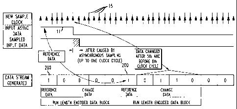
To achieve improved jitter performance within prescribed bandwidth
constraints, a receiver (140) samples a digital signal (11) upon each of n
periodic sample clock pulses that occur during the interval t, where n is
chosen such that log2(n+1) is an integer (x) greater than zero. At the each of
each interval t, the receiver generates a x+1-bit sample value having a first
bit indicating the value of the digital signal being sampled, and x remaining
bits which collectively indicate a sample interval during which the digital
signal changed states if such a change did occur When a change does occur, the
receiver inverts the first bit of each sample value upon decoding to coincide
with the change in the digital signal.


French Abstract

Selon cette invention, pour obtenir des effets de gigue réduits avec des contraintes données en matière de largeur de bande, un récepteur (140) échantillonne un signal numérique (11) à chaque n impulsion d'horloge d'échantillonnage périodique observée pendant l'intervalle t, n étant choisi de façon que log¿2?(n+1) désigne un nombre entier (x) supérieur à zéro. A la fin de chaque intervalle t, le récepteur génère une valeur d'échantillonnage de x+1 bits comprenant un premier bit indiquant la valeur du signal numérique en cours d'échantillonnage, et x bits restants qui indiquent collectivement un intervalle d'échantillonnage pendant lequel le signal numérique a changé d'état si un tel changement s'est effectivement produit. Lorsqu'un changement se produit, le récepteur inverse le premier bit de chaque valeur d'échantillonnage lors du décodage de façon qu'on obtienne une coïncidence avec le changement dans le signal numérique.

Claims

Note: Claims are shown in the official language in which they were submitted.


1. A method for sampling a digital signal yielding improved jitter performance
within
prescribed bandwidth constraints, comprising the steps of:
periodically sampling the digital signal n times during every interval t, with
n chosen such
that log2(n+1) is an integer (x) greater than zero, and t is chosen such that
the signal does not
undergo more than one change in state during such interval;
generating a x+1-bit sample value after each interval t, the sample value
having a first bit
indicating the binary value of the digital signal being sampled, and x
remaining bits which
collectively indicate a sub-interval during which the digital signal changed
states if such a change
did occur, and
inverting the first bit of each x+1 bit sample value upon decoding of the
sample to
coincide with the change in the digital signal.
2. The method according to claim 1 wherein n= 15 and x equals 4.
3. Apparatus for sampling a digital signal yielding improved jitter
performance
within prescribed bandwidth constraints, comprising of:
a sample clock for generating n periodic clock pulses during every interval t,
with n
chosen such that log2(n+1) is an integer (x) greater than zero and t is chosen
such that the signal
does not undergo more than one change in state during such interval;
a receiver for generating a x+1-bit sample value after each interval t, the
sample value
having a first bit indicating the binary value of the digital signal being
sampled, and x remaining
bits which collectively indicate a subinterval during which the digital signal
changed states if
such a change did occur, and the receiver inverting the first bit of each x+1
bit sample value upon
decoding of the sample to coincide with the change in the digital signal.
4. The apparatus according to claim 1 wherein n=15 and x equals 4.
-4-

Description

Note: Descriptions are shown in the official language in which they were submitted.


CA 02519308 2009-02-27
PU030092
OVERSAMPLING TECHNIQUE TO REDUCE JITTER
TECHNICAL FIELD
This invention relates to a technique for sampling an asynchronous digital
signal to
achieve reduced jitter performance
BACKGROUND ART
In various types of electronic systems, a need exists to sample a digital
signal to
determine its state, i.e., to determine whether the signal is at a logical "1
"or logical "0"
level. In practice, such sampling occurs periodically, typically in response
to a periodic
sample clock pulse. Ideally, sampling should occur at a sufficiently high
frequency to
minimize jitter, generally defined as the period of uncertainty between a
change in state of
the sampled signal and the next sample clock pulse. In a worst-case scenario,
the sampled
signal will change states just after the occurrence of a sample clock, so that
nearly an entire
sample clock interval will elapse before sampling the input signal again.
Increasing the sampling frequency will reduce the period of uncertainty and
thus
yield improved jitter performance. However, increasing the sampling frequency
will yield
more samples. In some electronic systems, bandwidth constraints limit the
number of
samples capable of being transmitted within a given interval. In such systems,
limited
opportunities exist for jitter performance improvement.
Thus, there is need for a technique that achieves increased jitter performance
in
bandwidth-limited systems.
BRIEF SUMMARY OF THE INVENTION
Briefly, in accordance with a preferred embodiment of the present principles,
there
is provided a method for sampling a digital signal that yields improved jitter
performance. The
method commences by sampling the digital signal n times during a given
interval, with n
chosen such that log2(n+l) is an integer x greater than zero. After each
interval t, an x+1 bit
data block is generated. The first bit represents the state of the sampled
signal, and the
1

CA 02519308 2009-02-27
PU030092
remaining x bits indicate the sample interval (i.e., the particular one of the
n clock pulses)
during which a change, if any, occurred. If a change did occur, then sample
value is
inverted upon decoding to coincide with the change in the sample value that
occurred
during the indicated sample interval.
BRIEF SUMMARY OF THE DRAWINGS
FIGURE 1 depicts a block schematic diagram of an apparatus in accordance with
the prior art for sampling an asynchronous digital signal;
FIGURE 2 depicts a time line showing the relationship over time among the
digital
signal undergoing sampling, the sample value obtained and the sample clock
pulses
generated by a sample clock comprising part of the apparatus of FIG. 1;
FIGURE 3 depicts a block schematic diagram of an apparatus in accordance with
the present principles for sampling an asynchronous digital signal with
improved jitter
performance; and
FIGURE 4 depicts a time line showing the relationship over time among the
digital
signal undergoing sampling, the sample value obtained and the sample clock
pulses
generated by a sample clock comprising part of the apparatus of FIG. 3.
DETAILED DESCRIPTION
FIGURE 1 depicts a prior art apparatus 10 for sampling an asynchronous digital
signal 11 generated by a transmitter 12. The transmitter 12 can take the form
of any type of
digital device that produces an asynchronous digital output signal. In other
words, the
output signal 11 of the transmitter 12 changes states between a logic "1 "
level and a logic
"0" level periodically. The sampling apparatus 10 includes a receiver 14
coupled to the
output of the transmitter 12 for detecting the state of the signal 11 in
response to each of a
sequence of periodic clock pulses 15 from a sample clock 16. The sample clock
16
generates m uniformly spaced clock pulses 15 during an interval of duration t.
In the
illustrated embodiment, m=5 although the value of m could be larger or
smaller.
FIGURE 2 depicts a timing chart that shows the relationship over time between
the output signal 11 of the transmitter 12 of FIG. 1 and the clock pulses 15
generated by the
sample clock 16 of FIG. 1. In the example depicted in FIG. 2, the signal 11
undergoes a
transition from a logic "1 " state to a logic "0" level shortly after the
occurrence of the second
2

CA 02519308 2010-09-16
PU030092
of the clock pulses 15 generated by the sample clock 16 of FIG. 1. Following
receipt of the
second clock pulse 15, the receiver 14 of FIG. I will again sample the signal
11. Upon
finding the signal 11 at a logic "1" level, the receiver 14 will maintain its
output signal 20 in
FIG. 2 at a logic "1" level as before. The output signal 20 of the receiver 14
remains at this
logic state until the next sampling interval following receipt of the next
(i.e., the third) clock
pulse 15. When clocked again by the sample clock 16 of FIG 1 (i.e., the fourth
clock pulse
occurrence), the receiver 14 of FIG. 2 now finds that the amplitude of the
signal 11 has
dropped to a logic "0" level. Accordingly, the receiver output signal 20 shown
in FIG. 2
now drops to a logic "0" level.
The shaded portion of the receiver output signal 20 depicted in FIG. 2
corresponds to
the lag between the change in state of the signal 11 and the change in state
of the receiver
output signal. This lag, referred to in the art as jitter, results from the
periodic sampling of
an asynchronous signal and can last up to one clock cycle. Increasing the
sampling rate (i.e.,
increasing the number of sample clock pulses per time interval t) will yield
more samples,
thus reducing the amount of jitter. However, some electronic systems have
bandwidth
constraints that limit the number of samples capable of being transmitted
during a given
interval. In such systems, the option of increasing the sampling rate to
improve jitter
performance does not exist.
FIGURE. 3 depicts a block schematic diagram of a system 100, in accordance
with a
preferred embodiment of the present principles, for sampling an asynchronous
digital signal
11 produced by transmitter 12 to achieve improved jitter performance while
maintaining
bandwidth constraints. The system 100 includes a receiver 140 that samples the
output signal
11 upon receipt of each of a sequence of periodic clock pulses 15 generated by
a clock 160.
As compared to the sample clock 16 of FIG. 1 which generates m uniformly
spaced periodic
pulses 15 during each interval t, the sample clock 160 of FIG. 3 generates n
uniformly spaced
pulses 15 during the same interval t where n > m. In the illustrated
embodiment, n=15,
although n could assume larger or smaller values, so long as log2(n+1) is an
integer x greater
than zero. Rather than generating a single bit sample value like the receiver
14 of FIG. 1, the
receiver 140 of FIG. 3 generates a sample comprised of an x+1 bit word 200
during each
interval t. The x+1 bit word 200 indicates the sample value of the signal 11
and also identifies
the particular one of the n clock cycles within the interval t during the
signal 11 underwent a
change in state if such a change did in fact occur.
3

CA 02519308 2010-09-16
PU030091
FIGURE 4 depicts a timing chart that shows the relationship over time between
the signal 11 generated by the transmitter 12 of FIG 2 and the pulses 15
generated by the
clock 160. As shown in FIG. 4, during each sample interval of duration t, the
receiver 140
of FIG. 1 receives a successive one of fifteen clock pulses 15, each pulse
causing the
receiver to sample the input signal 11. At the end of every interval t, the
receiver 140
generates a five-bit word 200 whose first bit (hereinafter referred to as a
"reference data"
bit) indicates the state of the input signal 11. The remaining four bits
collectively identity
the particular one of the fifteen clock cycles within the interval t during
which the signal 11
changed state, assuming such a change occurred.
As can be appreciated from the timing chart depicted in FIG. 4, the last four
bits of
the five-bit sample will uniquely identify each of the fifteen clock pulses
within the interval t.
Thus for example, the four-bit binary word (0 0 0 0) serves to identify the
first of the fifteen
pulses when there is no change in the fifteen-clock pulse period, whereas the
four bit-binary
word (1 1 1 1) identifies the fifteen' clock pulse when a change occurred at
that time. In
this way, the five-bit sample generated by the receiver 140 of FIG. 3 provides
a single
sample during each interval t with the same precision as fifteen individual
samples, thus,
improving jitter performance without violating bandwidth constraints. If a
change did occur
in the value of the signal, then sample value in the five-bit word 200 is
inverted upon
decoding to coincide with the change in the sample that occurred.
The sampling method performed by the receiver 140 constitutes a form of run-
length encoding which yields a single sample (referred to as a Run Length
Encoded Data
Block or RLEDB) of x bits in length with the same precision as n samples,
provided that
log2(n+l) = x. This scheme trades the maximum sample acquisition rate of a
given
communications link bandwidth for improved jitter performance. In the
illustrated
embodiment, a compression factor of 3.2-to-1 is achieved (16 samples in five
periods), so
jitter is reduced by the same ratio. Other compression factors are possible.
The only drawback of this method is that the signal 11 cannot undergo a change
in
state more than once during each interval t. In other words, the signal 11
cannot undergo
more than one change for each RLEDB. If the signal 11 were to change states
two or more
times per RLEDB, data will become lost.
The foregoing describes a technique for sampling an asynchronous signal with
improved jitter performance while maintaining bandwidth constraints.
4

Representative Drawing
A single figure which represents the drawing illustrating the invention.
Administrative Status

2024-08-01:As part of the Next Generation Patents (NGP) transition, the Canadian Patents Database (CPD) now contains a more detailed Event History, which replicates the Event Log of our new back-office solution.

Please note that "Inactive:" events refers to events no longer in use in our new back-office solution.

For a clearer understanding of the status of the application/patent presented on this page, the site Disclaimer , as well as the definitions for Patent , Event History , Maintenance Fee  and Payment History  should be consulted.

Event History

Description Date
Time Limit for Reversal Expired 2014-03-24
Letter Sent 2013-03-22
Revocation of Agent Requirements Determined Compliant 2011-12-16
Appointment of Agent Requirements Determined Compliant 2011-12-16
Inactive: Office letter 2011-12-15
Revocation of Agent Request 2011-11-30
Appointment of Agent Request 2011-11-30
Grant by Issuance 2011-11-01
Inactive: Cover page published 2011-10-31
Inactive: Final fee received 2011-08-23
Pre-grant 2011-08-23
Letter Sent 2011-04-27
Notice of Allowance is Issued 2011-02-28
Letter Sent 2011-02-28
Notice of Allowance is Issued 2011-02-28
Inactive: Approved for allowance (AFA) 2011-02-23
Revocation of Agent Requirements Determined Compliant 2011-02-22
Appointment of Agent Requirements Determined Compliant 2011-02-22
Inactive: Office letter 2011-02-22
Revocation of Agent Request 2011-02-15
Appointment of Agent Request 2011-02-15
Amendment Received - Voluntary Amendment 2010-09-16
Inactive: S.30(2) Rules - Examiner requisition 2010-07-07
Letter Sent 2009-04-16
Amendment Received - Voluntary Amendment 2009-02-27
Request for Examination Requirements Determined Compliant 2009-02-27
All Requirements for Examination Determined Compliant 2009-02-27
Request for Examination Received 2009-02-27
Inactive: IPRP received 2007-07-25
Letter Sent 2006-04-11
Inactive: Single transfer 2006-03-10
Inactive: Courtesy letter - Evidence 2005-11-15
Inactive: Cover page published 2005-11-10
Inactive: Notice - National entry - No RFE 2005-11-08
Application Received - PCT 2005-10-25
National Entry Requirements Determined Compliant 2005-09-15
Application Published (Open to Public Inspection) 2004-10-07

Abandonment History

There is no abandonment history.

Maintenance Fee

The last payment was received on 2011-03-02

Note : If the full payment has not been received on or before the date indicated, a further fee may be required which may be one of the following

  • the reinstatement fee;
  • the late payment fee; or
  • additional fee to reverse deemed expiry.

Patent fees are adjusted on the 1st of January every year. The amounts above are the current amounts if received by December 31 of the current year.
Please refer to the CIPO Patent Fees web page to see all current fee amounts.

Owners on Record

Note: Records showing the ownership history in alphabetical order.

Current Owners on Record
GVBB HOLDINGS S.A.R.L.
Past Owners on Record
ROBERT ALLEN CASTLEBARY
ROBERT LLOYD SHERMAN
Past Owners that do not appear in the "Owners on Record" listing will appear in other documentation within the application.
Documents

To view selected files, please enter reCAPTCHA code :


To view images, click a link in the Document Description column. To download the documents, select one or more checkboxes in the first column and then click the "Download Selected in PDF format (Zip Archive)" or the "Download Selected as Single PDF" button.

List of published and non-published patent-specific documents on the CPD .

If you have any difficulty accessing content, you can call the Client Service Centre at 1-866-997-1936 or send them an e-mail at CIPO Client Service Centre.


Document
Description 
Date
(yyyy-mm-dd) 
Number of pages   Size of Image (KB) 
Description 2005-09-14 4 222
Drawings 2005-09-14 2 38
Abstract 2005-09-14 1 71
Claims 2005-09-14 1 36
Representative drawing 2005-09-14 1 18
Claims 2005-09-15 1 47
Description 2009-02-26 4 211
Drawings 2010-09-15 2 38
Description 2010-09-15 4 212
Representative drawing 2011-09-26 1 11
Reminder of maintenance fee due 2005-11-22 1 109
Notice of National Entry 2005-11-07 1 192
Courtesy - Certificate of registration (related document(s)) 2006-04-10 1 128
Reminder - Request for Examination 2008-11-24 1 117
Acknowledgement of Request for Examination 2009-04-15 1 175
Commissioner's Notice - Application Found Allowable 2011-02-27 1 163
Maintenance Fee Notice 2013-05-02 1 171
PCT 2005-09-14 3 89
Correspondence 2005-11-07 1 28
PCT 2005-09-15 7 306
Correspondence 2011-02-14 4 117
Correspondence 2011-02-21 1 14
Correspondence 2011-08-22 1 39
Correspondence 2011-11-29 4 129
Correspondence 2011-12-14 1 20
Correspondence 2011-12-14 1 15