Note: Descriptions are shown in the official language in which they were submitted.
CA 02520625 2005-09-26
WO 2004/093146 PCT/US2004/011145
METHOD OF USING A MANHATTAN LAYOUT TO REALIZE NON
MANHATTAN SHAPED OPTICAL STRUCTURES
~1'~S~-~G'fGi'~FZC~ to Belated ~lpplicatiou
This application claims the benefit of Provisional Application 60/4619696,
filed April 10, 2003.
Techftical Field
The present invention relates to a layout tool compatible with IC industry
mask generation software packages and, more particularly, to a technique for
realizing
non-Manhattan geometries using Manhattan definitions, allowing for both
electronic
and optical components to be incorporated into the same mask set.
Background of the Ihvehtiou
As today's integrated circuit industry is based primarily on the use of
components with Manhattan geometries (i.e., 45° and 90° bends),
a challenge exists
for incorporating the layout of non-Manhattan planar optical components with
conventional electronic components. In particular, typical optical components
comprise elements such as splitters/combiners, waveguides, arrayed waveguide
structures, semiconductor optical amplifiers, Mach-Zehnder interferometers,
modulators, and the like, all requiring the use of bends and various angle
geometries.
As the photonic industry continues to mature, the need will arise to be able
to
fabricate these components using standard IC tools and processing techniques.
In
particular, the mask generation process will become a crucial step for
realizing optical
components using the same IC tools and processing as used in today's
microelectronics industry.
Additionally, a need exists in the optical simulation and modeling industry to
develop appropriate tools for efficiently importing and exporting optical
structures
without sacrificing the quality of the optical surfaces. A direct import of a
non-
Manhattan optical component from optical simulation software into an IC layout
tool
results in the conversion of the original non-Manhattan shape into low
resolution
discrete polygons. The currently available IC layout software packages have
limitations on the number of vertices they can use in order to generate the
imported
CA 02520625 2005-09-26
WO 2004/093146 PCT/US2004/011145
optical components. In the prior art, certain layout software packages
utilized for
either optical or IC applications are limited to only 4096 vertices, as a
result of their
12-bit operations. The limited number of vertices results in a modification of
the
optical component. This modification of the optical component during its
import to
the IC mask layout software can result in unexpected optical behavior that is
only
realized after the fabrication of the optical component. If the photon ics
industry is to
benefit from the high yield manufacturing model of the IC industry, the
import/export
limitations of the optical layout software packages needs to be addressed.
There also
remains the problem of providing a high resolution conversion of discrete
polygon
representations from set of input generating curves from mathematical
equations.
Summary of the Ihvehtiofz
The need remaining in the prior art is addressed by the present invention,
which relates to a layout tool compatible with IC industry mask generation
software
packages and, more particularly, to a technique for realizing non-Manhattan
geometries using Manhattan definitions, allowing for both electronic and
optical
components to be incorporated into the same mask set.
In accordance with the present invention, a complex-designed optical
component is realized by utilizing a plurality of contiguous polygons
(preferably,
rectangles), the vertices of adjacent polygons being fit to best meet the
contour of the
optical component. By increasing the number of polygons used to achieve the
fit (i.e.,
decreasing the size of each polygon), a better match is achieved. In the
limit, the
number of polygons is constrained only by the minimum grid spacing used for
mask
generation.
It is an advantage of the present invention that the "fitted rectangle" layout
technique is compatible with virtually any conventional IC software layout
package
and will continue to provide a higher resolution optical surface as the maslc
address
beam size decreases. Accordingly, the technique of the present invention
allows for
both optical and electronic components to be realized using the same mask
layout
process.
Other and further advantages of the present invention will become apparent
during the course of the present invention and by reference to the
accompanying
drawings.
2
CA 02520625 2005-09-26
WO 2004/093146 PCT/US2004/011145
BYief Desc~iptiotz of tlae Drawihgs
Referring now to the drawings,
FIG. 1 contains a high level system diagram illustrating the interaction of a
fitted rectangle optical component layout tool with a conventional mask
generation
tool and electronic component layout tool;
FIG. 2 illustrates an exemplary IC layout grid, illustrating the layout of a
first
set of components exhibiting a Manhattan geometry and a second set of
components
exhibiting a non-Manhattan geometry;
FIG. 3(a) is a prior art layout of a circle using currently available layout
tools,
and FIG. 3(b) is a layout of the same circle using the fitted rectangle
technique of the
present invention;
FIG. 4(a) is a prior art layout of an ellipse using currently available layout
tools, and FIG. 4(b) is a layout of the same ellipse using the fitted
rectangle technique
of the present invention;
FIG. 5 illustrates the use of a plurality of inscribed fitted rectangles to
define a
curve in accordance with the present invention;
FIG. 6 illustrates the use of a plurality of circumscribed fitted rectangles
to
define a curve in accordance with the present invention;
FIG. 7(a) is a prior art layout of a concave mirror using currently available
layout tools, and FIG. 7(b) is a layout of the same concave mirror using the
fitted
rectangle technique of the present invention;
FIG. 8(a) is a prior art layout of a taper using currently available layout
tools,
and FIG. 8(b) is a layout of the same taper using the fitted rectangle
technique of the
present invention; and
FIG. 9 illustrates the layout of an exemplary Mach Zehnder modulator.
Detailed Description
As mentioned above, the present invention relates to a method of fitting
vertices of polygons to generate optical components in a manner such that the
dimensions of the generated components, as well as the relational placement
between
components (particularly important when a waveguide needs to be located at a
mirror
focal point) is preserved with sufficient resolution during the import/export
of these
CA 02520625 2005-09-26
WO 2004/093146 PCT/US2004/011145
components between an optical simulation software package and an IC layout
software package. The process of the present invention involves the use of
individual
vertices (one or more) of a set of polygons that have been fit to a curve
outlining an
optical component. The optical component may then be generated using either an
equation of a geometrical shape or drawing using CAIN software. The fitted
vertices
of the polygons are chosen to match the grid used in the IC layout software.
Matching the grid enables efficient import and export of the optical
components
without any change in its physical dimensions. The format of the generated
files can
be configured to be compatible with the standard file formats used in the IC
industry.
Indeed, the method of the present invention is considered to be compatible
with
advancing methods of mask generation, such as Optical Proximity Correction
(OPC),
Extreme-Ultraviolet (EUV) and X-ray lithography. FIG. 1 illustrates, in
simplified
form, a system utilizing the present invention. An optical component simulator
I first
develops a physical layout of a set of various components in an optical
system, the
physical layout in proper dimensions with respect to the size of the
components, as
well as the spacing between the components. This information is then used as
an
input to a system 2 of fitting vertices of polygons to generate these shapes,
the system
being described in detail below. The output of system 2 is a layout in terms
of grid
spacing that is compatible with the layout tools currently in use for
electrical
integrated circuits. This layout information is applied as an input to a
conventional
mask layout system 3. An advantage of the present invention is that an
electronic
component simulator 4 may also provide layout information to mask layout
system 3,
so that both the optical and electrical components of a complicated system may
be
processed simultaneously within the mask layout tool.
FIG. 2 illustrates, for the sake of discussion, an exemplary IC layout tool
grid,
showing a layout of both Manhattan geometries (typically associated with
electronic
components) and non-Manhattan geometries (typically associated with optical
components). Electronic components 6 all comprise Manhattan geometries,
exhibiting straight lines interconnected by angles of either 90° or
45°. In contrast, the
non-Manhattan geometries of components 8 are seen to exhibit curved shapes
(including circular); various angles of connection, and tapered components.
These
various non-Manhattan geometries may be associated with conventional optical
components such as an optical grating, concave mirror, taper, lens, ring
resonator and
Mach-Zehnder interferometer. Indeed, the technique of the present invention is
4
CA 02520625 2005-09-26
WO 2004/093146 PCT/US2004/011145
considered to be particularly beneficial for the layout of diffractive optical
elements
(DOEs) that function to use the diffraction of light (as opposed to reflection
or
refraction) to provide the desired optical functionality. In particular, DOES
usually
consist of a large number of curved surfaces (one exemplary arrangement
comprising
~ series of concentric circles) that are difficult to Layout using
conventional Manhattan
arrangements. Thus, the method of the present invention, as described
hereinbelow
and particularly including Diffractive Optical Elements (DOE), enables these
various
optical components to be generated with conventional IC layout tools by
utilizing a
series of polygons (preferably, rectangles) to define the curved contours of
the optical
components.
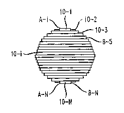
FIG. 3 illustrates the transfer of a circle into an IC layout tool, using the
process of the present invention. For the sake of comparison, FIG. 3 (a)
illustrates a
prior art circular shape generated using conventional optical component layout
tools,
where the circular shape is defined by using a polygonal structure. In
contrast, FIG.
3(b) illustrates a circular shape generated using the fitted polygon process
of the
present invention. For the purposes of the present discussion, it will be
presumed
hereinafter that a "rectangle" is used as the fitted polygon. As discussed
above, the
number of polygons used to fit a particular component is limited only by the
grid
spacing of the tool. It is to be understood that a rectangle is considered to
be only one
exemplary choice of a "fitting" polygon, and any other polygonal shape can be
used
in the inventive method, where the vertices of the selected polygon are
matched to lie
along the outline of the optical component. Referring to FIG. 3(b), a
plurality of
rectangles 10-1 through 10-N are used to fit the contour of the circular
shape. In
particular, vertices A and B of each rectangle 10-i is defined to coincide
with a point
on the grid spacing of the layout tool. In this manner, the circular shape is
more
accurately defined by the identified veuices than the prior art polygon shape
of FIG.
3(a).
In most cases, the wavelength of light used with a photonic lightwave platform
(for example, silicon, silica, InP or a polymer) is less than the wavelength
of light in a
vacuum. For example, the vacuum wavelength of 1.55 ~,m corresponds to a
wavelength of 0.44 ~,m in silicon waveguides. Therefore, based upon the
current
mask beam address, the spacing of vertices in a layout can be as small as 0.02
p,m. As
a result, the optical components generated by fitted rectangles in accordance
with the
CA 02520625 2005-09-26
WO 2004/093146 PCT/US2004/011145
present invention will be able to exhibit a high quality optical surface
(i.e., a x,120 or
better optical smoothness may be achieved).
FIG. 4 illustrates the layout of an exemplary elliptical optical component
(such
as a lens) using the fitted rectangle technique of the present invention,
where FIG.
4~(a) illustr~.tes the limitations of a prior art layout tool that utilizes
polygons to define
an optical component and FIG. 4(b), by comparison, illustrates the improvement
in
matching the elliptical contour by using the fitted rectangle technique of the
present
invention. As with the circular shape, a plurality of rectangles 12-1 through
12-M are
used to "fit" the contour of the ellipse, with vertices A and ~ of each
rectangle 12-i
selected to coincide with a point on the IC layout grid, as shown in FIG.
4(b). As
with each of the various layouts generated by the fitted rectangle technique
of the
present invention, the number of individual rectangles that may be used (as
controlled
by the grid spacing) is directly related to the "fit" that may be achieved.
FIG. S illustrates the use of a plurality of inscribed fitted rectangles 30-1
through 30-P to "fit" an exemplary curve 32 in accordance with the present
invention.
It is to be noted that the drawings of FIG. 5 is not drawn to scale, but has
been
enlarged for the sake of clarity. As shown, a set of vertices 34-1 through 34-
P are
defined as the grid points that coincide with curve 32. FIG. 6 illustrates, in
a similar
fashion (and also on an enlarged scale), the use of a plurality of
circumscribed fitted
rectangles 40-1 through 40-Q to "fit" an exemplary curve 42. Again, vertices
44-1
through 44-Q are defined as the grid points that coincide with curve 42. It is
to be
understood that either inscribed or circumscribed rectangles may be used to
provide
the desired fit, in accordance with the teachings of the present invention.
The layout of a concave mirror 50 using a plurality of fitted rectangles 52-1
through S2-R is illustrated in FIG. 7(b), where FIG. 7(a) shows the prior art
polygon
technique for the salve of comparison. As shown in FIG. 7(b), the height of
each
rectangle S2 is defined and limited by the minimum resolvable feature size of
the
mask being used for the layout. The length l of each rectangle is then
controlled such
that an associated vertex 54 is the best fit to the curve S6 of mirror S0. The
generation
of a linear taper 60 is illustrated in FIG. 8, with FIG. 8(a) illustrating a
prior art fit
technique using polygons, and the improvement obtained by using a plurality of
fitted
rectangles in accordance with the present invention, as shown in FIG. 8(b).
Referring
6
CA 02520625 2005-09-26
WO 2004/093146 PCT/US2004/011145
to FIG. 8(b), the length of each rectangle 62-1 through 62-S is controlled to
generate
the desired taper T for the particular linear taper 60.
It is to be understood that the above-described examples of the present
invention are presented only to illustrate the features of the present
invention in terms
of fitting a plurality of rectangles to defizxe the contour of any desired
optical
component for use with an IC layout tool. The layout of various other optical
components, or combination of optical components forming an optical subsystem,
for
example, may be generated using the fitted rectangle technique of the present
invention. In particular, FIG. ~ illustrates a layout of an optical device
consisting of a
Mach-Zehnder modulator 70 formed in accordance with the present invention. The
layout consists of planar mirrors 72, 74 to turn and focus the light into the
waveguide.
The sputters 76 and combiners 78 function to direct the light into and out of
the
separate, parallel waveguide arms 80, 82 forming the active region 84 of Mach-
Zehnder modulator 70. Since active region 84 of Mach-Zehnder modulator 70 also
includes active electronic devices to control the optical characteristics of
the guided
light, the mask level defines both the optical and electrical components (such
as by
using the system illustrated in FIG. 1). In summary, therefore, the scope of
the
present invention is intended to be limited only by the claims appended
hereto.
7