Note: Descriptions are shown in the official language in which they were submitted.
CA 02520672 2005-09-21
Internal reference: IRDM.O81 NON-EP / IDC-040046
SYSTEM AND METHOD FOR DISPLAY DEVICE WITH REINFORCING SUBSTANCE
Back rg ound
Field of the Invention
The field of the invention relates to microelectromechanical systems (MEMS).
More
specifically, the field of the invention relates to interferometric modulators
with a reinforcing
substance, e.g., a desiccant.
Descri~~tion of the Related Technolo~y
Microelectromechanical systems (MEMS) include micro mechanical elements,
actuators,
and electronics. Micromechanical elements may be created using deposition,
etching, and or
other micromachining processes that etch away parts of substrates and/or
deposited material
layers or that add layers to form electrical and electromechanical devices.
One type of MEMS
device is called an interferometric modulator. As used herein, the term
interferometric modulator
or interferometric light modulator refers to a device that selectively absorbs
and/or reflects light
using the principles of optical interference. In certain embodiments, an
interferometric modulator
may comprise a pair of conductive plates, one or both of which may be
transparent and/or
reflective in whole or part and capable of relative motion upon application of
an appropriate
electrical signal. In a particular embodiment, one plate may comprise a
stationary layer
deposited on a substrate and the other plate may comprise a metallic membrane
separated from
the stationary layer by an air gap. As described herein in more detail, the
position of one plate in
relation to another can change the optical interference of light incident on
the interferometric
modulator. Such devices have a wide range of applications, and it would be
beneficial in the art
to utilize and/or modify the characteristics of these types of devices so that
their features can be
exploited in improving existing products and creating new products that have
not yet been
developed.
Summary of Certain Embodiments
One embodiment of the invention is a display device, comprising: a transparent
substrate;
an interferometric modulator configured to modulate light transmitted through
the transparent
substrate; a backplate sealed to said transparent substrate to form a package,
wherein said
interferometric modulator is inside said package; and a reinforcing substance
in contact with said
backplate, wherein said reinforcing substance is configured to provide
structural support to the
backplate.
CA 02520672 2005-09-21
Yet another embodiment of the invention is a display device, comprising:
transmissive
means for transmitting light therethrough; modulating means for modulating
light transmitted
through the transmissive means; covering means sealed to said transmissive
means to form a
package, wherein said modulating means is inside said package; and reinforcing
means the
backplate.
Still another embodiment of the invention is a method of manufacturing a
display device,
comprising: providing a transparent substrate comprising an interferometric
modulator
configured to modulate light transmitted through the transparent substrate;
providing a backplate
configured to mount to said transparent substrate; applying a reinforcing
substance to said
backplate, wherein said reinforcing substance is configured to provide
structural support to said
backplate, and sealing said backplate to said transparent substrate.
One other embodiment of the invention is a display device manufactured by the
method
of: providing a transparent substrate comprising an interferometric modulator
configured to
modulate light transmitted through the transparent substrate; providing a
backplate configured to
mount to said transparent substrate; applying a reinforcing substance to said
backplate, wherein
said reinforcing substance is configured to provide structural support to said
backplate, and
sealing said backplate to said transparent substrate.
Brief Description of the Drawings
Figure 1 is an isometric view depicting a portion of one embodiment of an
interferometric modulator display in which a movable reflective layer of a
first interferometric
modulator is in a released position and a movable reflective layer of a second
interferometric
modulator is in an actuated position.
Figure 2 is a system block diagram illustrating one embodiment of an
electronic device
incorporating a 3x3 interferometric modulator display.
Figure 3 is a diagram of movable mirror position versus applied voltage for
one
exemplary embodiment of an interferometric modulator of Figure 1.
Figure 4 is an illustration of a set of row and column voltages that may be
used to drive
an interferometric modulator display.
Figure SA illustrates one exemplary frame of display data in the 3x3
interferometric
modulator display of Figure 2.
Figure SB illustrates one exemplary timing diagram for row and column signals
that may
be used to write the frame of Figure SA.
Figure 6A is a system block diagram illustrating an embodiment of a display
device.
Figure 6B is a system block diagram illustrating some of the components of an
embodiment of a display device.
-2-
CA 02520672 2005-09-21
Figure 7A is a cross section of the device of Figure 1.
Figure 7B is a cross section of an alternative embodiment of an
interferometric
modulator.
Figure 7C is a cross section of another alternative embodiment of an
interferometric
modulator.
Figure 8 schematically illustrates a front view of one embodiment of a
wireless telephone
handset having an electronic display.
Figure 9 schematically illustrates a perspective view of one embodiment of an
electronic
display.
Figure 10 schematically illustrates a cross-sectional view of one embodiment
of an
electronic display taken across the line 3-3 from Figure 9.
Figure 11 schematically illustrates a first alternate embodiment of an
electronic display
taken across the line 3-3 from Figure 9.
Figure 12 schematically illustrates one or more embodiments of how the
reinforcing
substance can be used to add support or increase the integrity of the
backplate.
Figure 13 schematically illustrates an alternative embodiment of how the
reinforcing
substance can add support to the backplate.
Figure 14A schematically illustrates one embodiment of how a reinforcing
substance can
be configured.
Figure 14B schematically illustrates another embodiment of how a reinforcing
substance
can be configured.
Figure 14C schematically illustrates another embodiment of how a reinforcing
substance
can be configured.
Figure 14D schematically illustrates another embodiment of how a reinforcing
substance
can be configured.
Figure 15A is a graph depicting the rates of water absorption for HiCap2800TM
desiccant,
a prolonged acting desiccant.
Figure 15B is a graph depicting the rates of water absorption for Bondline
Zeolite
desiccant, a fast acting desiccant.
Figure 16 is a graph comparing the percent weight gain for ZeoliteTM and
StayDry
HiCapTM desiccants.
Detailed Description of Certain Embodiments
The following detailed description is directed to certain specific embodiments
of the
invention. However, the invention can be embodied in a multitude of different
ways. In this
description, reference is made to the drawings wherein like parts are
designated with like
-3-
CA 02520672 2005-09-21
numerals throughout. As will be apparent from the following description, the
embodiments may
be implemented in any device that is configured to display an image, whether
in motion (e.g.,
video) or stationary (e.g., still image), and whether textual or pictorial.
More particularly, it is
contemplated that the embodiments may be implemented in or associated with a
variety of
electronic devices such as, but not limited to, mobile telephones, wireless
devices, personal data
assistants (PDAs), hand-held or portable computers, GPS receivers/navigators,
cameras, MP3
players, camcorders, game consoles, wrist watches, clocks, calculators,
television monitors, flat
panel displays, computer monitors, auto displays (e.g., odometer display,
etc.), cockpit controls
and/or displays, display of camera views (e.g., display of a rear view camera
in a vehicle),
electronic photographs, electronic billboards or signs, projectors,
architectural structures,
packaging, and aesthetic structures (e.g., display of images on a piece of
jewelry). MEMS
devices of similar structure to those described herein can also be used in non-
display applications
such as in electronic switching devices.
In some aspects, the invention is a reinforcing substance on the surface of a
backplate in
a package of an interferometric modulator. The reinforcing aspect of the
substance can be
achieved in a variety of ways. For example, the reinforcing substrate can fill
variations or
imperfections in the backplate and thereby provide additional structural
support. Alternatively,
the reinforcing substance can form a reinforcing structure in itself, which
can add additional
strength to the backplate. This can allow for thinner backplates to be used.
In one embodiment,
the reinforcing substance is a desiccant. In another embodiment, the desiccant
is a prolonged
acting or long acting desiccant, which, while not necessarily absorbing large
amounts of water
immediately, is able to absorb water over a relatively prolonged period of
time. In some
embodiments, the desiccant is covered by a barrier that reduces the amount of
water that is
exposed to the desiccant and thereby extends the effective lifetime of the
desiccant. In some
embodiments the desiccant is positioned selectively on the backplate to add
support to weak
points on the backplate, e.g., on the corners of the backplate. Methods of
making and using these
embodiments are also contemplated.
One interferometric modulator display embodiment comprising an interferometric
MEMS display element is illustrated in Figure 1. In these devices, the pixels
are in either a
bright or dark state. In the bright ("on" or "open") state, the display
element reflects a large
portion of incident visible light to a user. When in the dark ("off ' or
"closed") state, the display
element reflects little incident visible light to the user. Depending on the
embodiment, the light
reflectance properties of the "on" and "ofF' states may be reversed. MEMS
pixels can be
configured to reflect predominantly at selected colors, allowing for a color
display in addition to
black and white.
-4-
CA 02520672 2005-09-21
Figure 1 is an isometric view depicting two adjacent pixels in a series of
pixels of a
visual display, wherein each pixel comprises a MEMS interferometric modulator.
In some
embodiments, an interferometric modulator display comprises a row/column array
of these
interferometric modulators. Each interferometric modulator includes a pair of
reflective layers
positioned at a variable and controllable distance from each other to form a
resonant optical
cavity with at least one variable dimension. In one embodiment, one of the
reflective layers may
be moved between two positions. In the first position, referred to herein as
the relaxed, the
movable layer is positioned at a relatively large distance from a fixed
partially reflective layer. In
the second position, the movable layer is positioned more closely adjacent to
the partially
reflective layer. Incident light that reflects from the two layers interferes
constructively or
destructively depending on the position of the movable reflective layer,
producing either an
overall reflective or non-reflective state for each pixel.
The depicted portion of the pixel array in Figure 1 includes two adjacent
interferometric
modulators 12a and 12b. In the interferometric modulator 12a on the left, a
movable and highly
reflective layer 14a is illustrated in a relaxed position at a predetermined
distance from a fixed
partially reflective layer 16a. In the interferometric modulator 12b on the
right, the movable
highly reflective layer 14b is illustrated in an actuated position adjacent to
the fixed partially
reflective layer 16b.
The fixed layers 16a, 16b are electrically conductive, partially transparent
and partially
reflective, and may be fabricated, for example, by depositing one or more
layers each of
chromium and indium-tin-oxide onto a transparent substrate 20. The layers are
patterned into
parallel strips, and may form row electrodes in a display device as described
further below. The
movable layers 14a, 14b may be formed as a series of parallel strips of a
deposited metal layer or
layers (orthogonal to the row electrodes 16a, 16b) deposited on top of posts
18 and an intervening
sacrificial material deposited between the posts 18. When the sacrificial
material is etched away,
the deformable metal layers 14a, 14b are separated from the fixed metal layers
by a defined gap
19. A highly conductive and reflective material such as aluminum may be used
for the
deformable layers, and these strips may form column electrodes in a display
device.
With no applied voltage, the cavity 19 remains between the layers 14a, 16a and
the
deformable layer is in a mechanically relaxed state as illustrated by the
pixel 12a in Figure 1.
However, when a potential difference is applied to a selected row and column,
the capacitor
formed at the intersection of the row and column electrodes at the
corresponding pixel becomes
charged, and electrostatic forces pull the electrodes together. If the voltage
is high enough, the
movable layer is deformed and is forced against the fixed layer (a dielectric
material which is not
illustrated in this Figure may be deposited on the fixed layer to prevent
shorting and control the
separation distance) as illustrated by the pixel 12b on the right in Figure 1.
The behavior is the
-5-
CA 02520672 2005-09-21
same regardless of the polarity of the applied potential difference. In this
way, row/column
actuation that can control the reflective vs. non-reflective pixel states is
analogous in many ways
to that used in conventional LCD and other display technologies.
Figures 2 through SB illustrate one exemplary process and system for using an
array of
interferometric modulators in a display application.
Figure 2 is a system block diagram illustrating one embodiment of an
electronic device
that may incorporate aspects of the invention. In the exemplary embodiment,
the electronic
device includes a processor 21 which may be any general purpose single- or
multi-chip
microprocessor such as an ARM, Pentium~, Pentium II~, Pentium I1I~, Pentium
IV~, Pentium~
Pro, an 8051, a MIPS~, a Power PC~, an ALPHA~, or any special purpose
microprocessor such
as a digital signal processor, microcontroller, or a programmable gate array.
As is conventional
in the art, the processor 21 may be configured to execute one or more software
modules. In
addition to executing an operating system, the processor may be configured to
execute one or
more software applications, including a web browser, a telephone application,
an email program,
or any other software application.
In one embodiment, the processor 21 is also configured to communicate with an
array
controller 22. In one embodiment, the array controller 22 includes a row
driver circuit 24 and a
column driver circuit 26 that provide signals to a display array or panel 30.
The cross section of
the array illustrated in Figure 1 is shown by the lines 1-1 in Figure 2. For
MEMS interferometric
modulators, the row/column actuation protocol may take advantage of a
hysteresis property of
these devices illustrated in Figure 3. 1t may require, for example, a 10 volt
potential difference to
cause a movable layer to deform from the relaxed state to the actuated state.
However, when the
voltage is reduced from that value, the movable layer maintains its state as
the voltage drops back
below 10 volts. In the exemplary embodiment of Figure 3, the movable layer
does not relax
completely until the voltage drops below 2 volts. There is thus a range of
voltage, about 3 to 7 V
in the example illustrated in Figure 3, where there exists a window of applied
voltage within
which the device is stable in either the relaxed or actuated state. This is
referred to herein as the
"hysteresis window" or "stability window." For a display array having the
hysteresis
characteristics of Figure 3, the row/column actuation protocol can be designed
such that during
row strobing, pixels in the strobed row that are to be actuated are exposed to
a voltage difference
of about 10 volts, and pixels that are to be relaxed are exposed to a voltage
difference of close to
zero volts. After the strobe, the pixels are exposed to a steady state voltage
difference of about 5
volts such that they remain in whatever state the row strobe put them in.
After being written,
each pixel sees a potential difference within the "stability window" of 3-7
volts in this example.
This feature makes the pixel design illustrated in Figure 1 stable under the
same applied voltage
conditions in either an actuated or relaxed pre-existing state. Since each
pixel of the
-6-
CA 02520672 2005-09-21
interferometric modulator, whether in the actuated or relaxed state, is
essentially a capacitor
formed by the fixed and moving reflective layers, this stable state can be
held at a voltage within
the hysteresis window with almost no power dissipation. Essentially no current
flows into the
pixel if the applied potential is fixed.
In typical applications, a display frame may be created by asserting the set
of column
electrodes in accordance with the desired set of actuated pixels in the first
row. A row pulse is
then applied to the row 1 electrode, actuating the pixels corresponding to the
asserted column
lines. The asserted set of column electrodes is then changed to correspond to
the desired set of
actuated pixels in the second row. A pulse is then applied to the row 2
electrode, actuating the
appropriate pixels in row 2 in accordance with the asserted column electrodes.
The row I pixels
are unaffected by the row 2 pulse, and remain in the state they were set to
during the row 1 pulse.
This may be repeated for the entire series of rows in a sequential fashion to
produce the frame.
Generally, the frames are refreshed and/or updated with new display data by
continually
repeating this process at some desired number of frames per second. A wide
variety of protocols
for driving row and column electrodes of pixel arrays to produce display
frames are also well
known and may be used in conjunction with the present invention.
Figures 4, SA and SB illustrate one possible actuation protocol for creating a
display
frame on the 3x3 array of Figure 2. Figure 4 illustrates a possible set of
column and row voltage
levels that may be used for pixels exhibiting the hysteresis curves of Figure
3. In the Figure 4
embodiment, actuating a pixel involves setting the appropriate column to -
Vb;as, and the
appropriate row to +pV, which may correspond to -5 volts and +5 volts
respectively Relaxing
the pixel is accomplished by setting the appropriate column t0 +Vb;as, and the
appropriate row to
the same +~V, producing a zero volt potential difference across the pixel. In
those rows where
the row voltage is held at zero volts, the pixels are stable in whatever state
they were originally
in, regardless of whether the column is at +Vb;as, or -Vb;as. As is also
illustrated in Figure 4, it will
be appreciated that voltages of opposite polarity than those described above
can be used, e.g.,
actuating a pixel can involve setting the appropriate column t0 +Vb;as, and
the appropriate row to
-0V. In this embodiment, releasing the pixel is accomplished by setting the
appropriate column
to -Vb;as, and the appropriate row to the same -4V, producing a zero volt
potential difference
across the pixel.
Figure SB is a timing diagram showing a series of row and column signals
applied to the
3x3 array of Figure 2 which will result in the display arrangement illustrated
in Figure SA, where
actuated pixels are non-reflective. Prior to writing the frame illustrated in
Figure SA, the pixels
can be in any state, and in this example, all the rows are at 0 volts, and all
the columns are at +5
volts: With these applied voltages, all pixels are stable in their existing
actuated or relaxed states.
CA 02520672 2005-09-21
1n the Figure SA frame, pixels (1,1), (1,2), (2,2), (3,2) and (3,3) are
actuated. To
accomplish this, during a "line time" for row 1, columns 1 and 2 are set to -5
volts, and column 3
is set to +5 volts. This does not change the state of any pixels, because all
the pixels remain in
the 3-7 volt stability window. Row 1 is then strobed with a pulse that goes
from 0, up to 5 volts,
and back to zero. This actuates the (1,1) and (1,2) pixels and relaxes the
(1,3) pixel. No other
pixels in the array are affected. To set row 2 as desired, column 2 is set to -
5 volts, and columns
1 and 3 are set to +5 volts. The same strobe applied to row 2 will then
actuate pixel (2,2) and
relax pixels (2,1) and (2,3). Again, no other pixels of the array are
affected. Row 3 is similarly
set by setting columns 2 and 3 to -5 volts, and column 1 to +5 volts. The row
3 strobe sets the
row 3 pixels as shown in Figure SA. After writing the frame, the row
potentials are zero, and the
column potentials can remain at either +5 or -5 volts, and the display is then
stable in the
arrangement of Figure SA. It will be appreciated that the same procedure can
be employed for
arrays of dozens or hundreds of rows and columns. It will also be appreciated
that the timing,
sequence, and levels of voltages used to perform row and column actuation can
be varied widely
within the general principles outlined above, and the above example is
exemplary only, and any
actuation voltage method can be used with the systems and methods described
herein.
Figures 6A and 6B are system block diagrams illustrating an embodiment of a
display
device 40. The display device 40 can be, for example, a cellular or mobile
telephone. However,
the same components of display device 40 or slight variations thereof are also
illustrative of
various types of display devices such as televisions and portable media
players.
The display device 40 includes a housing 41, a display 30, an antenna 43, a
speaker 44,
an input device 48, and a microphone 46. The housing 41 is generally formed
from any of a
variety of manufacturing processes as are well known to those of skill in the
art, including
injection molding, and vacuum forming. In addition, the housing 41 may be made
from any of a
variety of materials, including but not limited to plastic, metal, glass,
rubber, and ceramic, or a
combination thereof. In one embodiment the housing 41 includes removable
portions (not
shown) that may be interchanged with other removable portions of different
color, or containing
different logos, pictures, or symbols.
The display 30 of exemplary display device 40 may be any of a variety of
displays,
including a bi-stable display, as described herein. In other embodiments, the
display 30 includes a
flat-panel display, such as plasma, EL, OLED, STN LCD, or TFT LCD as described
above, or a
non-flat-panel display, such as a CRT or other tube device, as is well known
to those of skill in
the art. However, for purposes of describing the present embodiment, the
display 30 includes an
interferometric modulator display, as described herein.
The components of one embodiment of exemplary display device 40 are
schematically
illustrated in Figure 6B. The illustrated exemplary display device 40 includes
a housing 41 and
_g_
CA 02520672 2005-09-21
can include additional components at least partially enclosed therein. For
example, in one
embodiment, the exemplary display device 40 includes a network interface 27
that includes an
antenna 43 which is coupled to a transceiver 47. The transceiver 47 is
connected to a processor
21, which is connected to conditioning hardware 52. The conditioning hardware
52 may be
configured to condition a signal (e.g. filter a signal). The conditioning
hardware 52 is connected
to a speaker 44 and a microphone 46. The processor 21 is also connected to an
input device 48
and a driver controller 29. The driver controller 29 is coupled to a frame
buffer 28, and to an
array driver 22, which in turn is coupled to a display array 30. A power
supply 50 provides
power to all components as required by the particular exemplary display device
40 design.
The network interface 27 includes the antenna 43 and the transceiver 47 so
that the
exemplary display device 40 can communicate with one ore more devices over a
network. In one
embodiment the network interface 27 may also have some processing capabilities
to relieve
requirements of the processor 21. The antenna 43 is any antenna known to those
of skill in the
art for transmitting and receiving signals. In one embodiment, the antenna
transmits and receives
RF signals according to the IEEE 802.11 standard, including IEEE 802.11(a),
(b), or (g). In
another embodiment, the antenna transmits and receives RF signals according to
the
BLUETOOTH standard. In the case of a cellular telephone, the antenna is
designed to receive
CDMA, GSM, AMPS or other known signals that are used to communicate within a
wireless cell
phone network. The transceiver 47 pre-processes the signals received from the
antenna 43 so that
they may be received by and further manipulated by the processor 21. The
transceiver 47 also
processes signals received from the processor 21 so that they may be
transmitted from the
exemplary display device 40 via the antenna 43.
In an alternative embodiment, the transceiver 47 can be replaced by a
receiver. In yet
another alternative embodiment, network interface 27 can be replaced by an
image source, which
can store or generate image data to be sent to the processor 21. For example,
the image source
can be a digital video disc (DVD) or a hard-disc drive that contains image
data, or a software
module that generates image data.
Processor 21 generally controls the overall operation of the exemplary display
device 40.
The processor 21 receives data, such as compressed image data from the network
interface 27 or
an image source, and processes the data into raw image data or into a format
that is readily
processed into raw image data. The processor 21 then sends the processed data
to the driver
controller 29 or to frame buffer 28 for storage. Raw data typically refers to
the information that
identifies the image characteristics at each location within an image. For
example, such image
characteristics can include color, saturation, and gray-scale level.
In one embodiment, the processor 21 includes a microcontroller, CPU, or logic
unit to
control operation of the exemplary display device 40. Conditioning hardware 52
generally
-9-
CA 02520672 2005-09-21
includes amplifiers and filters for transmitting signals to the speaker 44,
and for receiving signals
from the microphone 46. Conditioning hardware 52 may be discrete components
within the
exemplary display device 40, or may be incorporated within the processor 21 or
other
components.
The driver controller 29 takes the raw image data generated by the processor
21 either
directly from the processor 21 or from the frame buffer 28 and reformats the
raw image data
appropriately for high speed transmission to the array driver 22.
Specifically, the driver
controller 29 reformats the raw image data into a data flow having a raster-
like format, such that
it has a time order suitable for scanning across the display array 30. Then
the driver controller 29
sends the formatted information to the array driver 22. Although a driver
controller 29, such as a
LCD controller, is often associated with the system processor 21 as a stand-
alone Integrated
Circuit (IC), such controllers may be implemented in many ways. They may be
embedded in the
processor 21 as hardware, embedded in the processor 21 as software, or fully
integrated in
hardware with the array driver 22.
Typically, the array driver 22 receives the formatted information from the
driver
controller 29 and reformats the video data into a parallel set of waveforms
that are applied many
times per second to the hundreds and sometimes thousands of leads coming from
the display's x-
y matrix of pixels.
In one embodiment, the driver controller 29, array driver 22, and display
array 30 are
appropriate for any of the types of displays described herein. For example, in
one embodiment,
driver controller 29 is a conventional display controller or a bi-stable
display controller (e.g., an
interferometric modulator controller). In another embodiment, array driver 22
is a conventional
driver or a bi-stable display driver (e.g., an interferometric modulator
display). In one
embodiment, a driver controller 29 is integrated with the array driver 22.
Such an embodiment is
common in highly integrated systems such as cellular phones, watches, and
other small area
displays. In yet another embodiment, display array 30 is a typical display
array or a bi-stable
display array (e.g., a display including an array of interferometric
modulators).
The input device 48 allows a user to control the operation of the exemplary
display
device 40. In one embodiment, input device 48 includes a keypad, such as a
QWERTY keyboard
or a telephone keypad, a button, a switch, a touch-sensitive screen, a
pressure- or heat-sensitive
membrane. In one embodiment, the microphone 46 is an input device for the
exemplary display
device 40. When the microphone 46 is used to input data to the device, voice
commands may be
provided by a user for controlling operations of the exemplary display device
40.
Power supply 50 can include a variety of energy storage devices as are well
known in the
art. For example, in one embodiment, power supply 50 is a rechargeable
battery, such as a
nickel-cadmium battery or a lithium ion battery. In another embodiment, power
supply 50 is a
-10-
CA 02520672 2005-09-21
renewable energy source, a capacitor, or a solar cell, including a plastic
solar cell, and solar-cell
paint. In another embodiment, power supply 50 is configured to receive power
from a wall
outlet.
In some implementations control programmability resides, as described above,
in a driver
controller which can be located in several places in the electronic display
system. In some cases
control programmability resides in the array driver 22. Those of skill in the
art will recognize
that the above-described optimization may be implemented in any number of
hardware and/or
software components and in various configurations.
The details of the structure of interferometric modulators that operate in
accordance with
the principles set forth above may vary widely. For example, Figures 7A-7C
illustrate three
different embodiments of the moving mirror structure. Figure 7A is a cross
section of the
embodiment of Figure 1, where a strip of metal material 14 is deposited on
orthogonally
extending supports 18. In Figure 7B, the moveable reflective material 14 is
attached to supports
at the corners only, on tethers 32. In Figure 7C, the moveable reflective
material 14 is suspended
from a deformable layer 34. This embodiment has benefits because the
structural design and
materials used for the reflective material 14 can be optimized with respect to
the optical
properties, and the structural design and materials used for the deformable
layer 34 can be
optimized with respect to desired mechanical properties. The production of
various types of
interferometric devices is described in a variety of published documents,
including, for example,
U.S. Published Application 2004/0051929. A wide variety of known techniques
may be used to
produce the above described structures involving a series of material
deposition, patterning, and
etching steps.
As discussed above, in some embodiments, the invention can be used in
electronic
displays for use in portable electronic devices, such as wireless telephones,
personal digital
assistants, computer monitors, digital music players and the like. Figure 8
illustrates a wireless
telephone handset 110 having an electronic display 120. In this illustration,
the electronic display
120 is displaying the telephone number "555-1212".
Electronic display 120 can be any type of display including light emitting
diode (LED),
organic light emitting diode (OLED), or an interferometric modulator (IMOD)
direct view
electronic display.
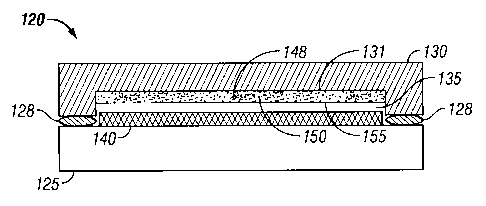
Figure 10 shows a perspective view of the display 120 from Figure 9. As shown,
the
display 120 has a transparent front surface 125, a sealant 128, and a
backplate 130. As will be
explained below, within the display 110, and between the transparent front
surface 125 and
backplate 130 are the electronics for the particular display technology. For
example, within the
display can be the electronics for an LED, OLED or IMOD display.
CA 02520672 2005-09-21
Interferometric displays, which are based on MEMS (micro-electro-mechanical-
systems)
technology, are spatial light modulators that may be used in electronic
display applications, such
as a wireless telephone handset. Interferometric modulators modulate light by
controlling the
self interference of light that strikes a surface of the modulator. For
example, U.S. Patent No.
5,835,255 discloses one example of an interferometric modulator which is
hereby incorporated
by reference in its entirety.
Reinforcing Substance
While the size of the backplate 130 can be miniaturized to allow for smaller
display
devices, this results in a thinner backplate which could be relatively weak.
Additionally, some
manufacturing processes can leave minor imperfections in the backplate, which
may weaken the
structure as well. Thus, stronger backplates to allow for smaller devices can
be desirable.
Additionally, it should be realized that each of the above display types are
differentially sensitive
to moisture. Thus it can be advantageous to provide a means for reducing the
amount of moisture
that may come in contact with the device.
As mentioned above, aspects of the invention relate to the manufacturing and
packaging
of electronic displays with a reinforcing substance. The reinforcing substance
is configured to
add structural support to the package. The reinforcing substance can also be
configured to absorb
water molecules that permeate the display packaging once it has been
manufactured, e.g., it can
be a desiccant. As will be appreciated by one of skill in the art, a desiccant
maintains a low
humidity environment within the display package and prevents water vapor from
adversely
affecting the operation of the display electronics. This will be explained in
further detail below.
Interferometric modulators typically include a transparent substrate, such as
glass, as well
as moving parts that have a protected space in which to move. A schematic of a
basic package
structure for an interferometric modulator is illustrated in Figure 10,
although it should be
realized that the invention is not limited to packaging a particular type of
display or the use of a
particular substrate material, such as glass. As shown in Figure 10, a basic
package structure
includes the transparent substrate 125 and the backplate or "cap" 130. These
components are
held together by the sealant 128, but provide a cavity 135 formed between
these two components.
Within the cavity 135 and adjacent the transparent substrate 125 is an
interferometric modulator
140. As illustrated, the cavity 135 can also be provided by the use of a
backplate glass that has
a recessed cavity. Using a recessed cavity 135 allows the sealant material 128
to be relatively
thin, and thus not be as subject to transmission of water vapor. An
alternative package structure
is shown in Figure 1 I.
The transparent substrate 125 can be any transparent substance capable of
having display
electronics, such as a thin film MEMS device built upon it. Such transparent
substances include,
-12-
CA 02520672 2005-09-21
but are not limited to, glass, plastic, and transparent polymers. Images are
displayed through the
substrate 125, which serves as an imaging surface. The interferometric
modulator array may
comprise membrane modulators or modulators of the separable type. Examples of
such devices
are described in U.S. Patent No. 5,835,255 to Miles. The skilled artisan will
appreciate that the
backplate 130 can be formed of any suitable material, such as glass, metal,
foil, polymer, plastic,
ceramic, or semiconductor materials (e.g., silicon).
The interferometric modulator 140 can be a membrane modulator or modulators of
the
separable type. Examples of such devices are described in U.S. Patent
5,835,255 to Miles,
hereby incorporated in its entirety by reference.
As will be appreciated by one of skill in the art, the backplate 130 can
independently be
strong enough so that the integrity of the packaging system is not
compromised, either throughout
the manufacture or throughout the use of the device. However, as discussed in
more detail
below, the dimensions, shape, composition, and other characteristics of the
backplate can be
altered depending on the presence or absence of a reinforcing substance in the
package.
Especially when moving to larger display diagonals, reinforcement of the
package allows for the
manufacture of a relatively thin display. In addition, reinforcement of the
package maintains a
minimum bowing of the recessed glass to the order or 100-200 micron when
moderate pressure is
applied to the backplate. Thus, in some embodiments, in which a reinforcing
substance is to be
used, a backplate can be thinner or may be insufficient to independently
maintain the structural
integrity of the packaging system. In other embodiments, the reinforcing
substance can simply
add additional strength to the system or other desired characteristics, such
as a drying ability, or
both characteristics. This backplate 130 may also be referred to as a
"backplane." It will be
understood that the terms "display," "package structure," and "package" can be
used
interchangeably, as used herein.
The sealant or seal 128 is typically provided to join the transparent
substrate 125 and
backplate 130 to form the package structure 120. The sealant 128 is typically
a non-hermetic
seal, such as a conventional epoxy-based adhesive. In addition, the sealant
128 may be made
from any polymer, or plastic composition. In one embodiment, the sealant 128
provides a
hermetic seal that prevents water vapor and moisture from entering the cavity
135. In other
embodiments, the seal 128 can be a polyisobutylene (sometimes called butyl
rubber, and other
times PIB), o-rings, polyurethane, thin film metal weld, liquid spin-on glass,
or solder, among
other types of seals that can have a range of permeability of water vapor of
about 0.2 - 4.7 g
mm/mzkPa day.
As shown in Figure 10, there is a cavity 135 between the backplate 130 and the
substrate
125. The moving parts of a MEMS device, such as the movable mirrors 14a, 14b
of an
interferometric modulator array described above, preferably have a protected
space in which to
-13-
CA 02520672 2005-09-21
move. As illustrated in Figure 10, the cavity 135 can be provided by the use
of a backplate 130
that has a recessed cavity.
It has been realized that the addition of an additional reinforcing substance
to the
backplate can be useful in providing additional strength to the backplate
without necessarily
requiring the greater space required by a thicker backplate.
The reinforcing substance can be selected from a variety of substances. The
reinforcing
substance can be an epoxy, a desiccant, or some combination thereof. In light
of the present
disclosure, one of skill in the art will be able to determine appropriate
substances, how to prepare,
and how to use them. For example, pastes can be prepared by mixing a Ca0
desiccant or Zeolite
desiccant with a polymeric binder. An example of a desiccant paste is the
commercially available
Cookson HiCap 2800TM desiccant paste. This paste can be screen printed or
dispensed onto the
backplate. 1t can have a thin sheet on the order of 50 microns for example, or
various shapes and
patterns, as described in more detail below. The paste can be heated and
activated after
dispensing. Another type, a Zeolite based paste for example, can be spread in
a similar way, but
may not require heating or activated after application. As described in more
detail below, the
reinforcing substance provides structural support to the package. This support
can be due to, for
example, the strength and integrity of the reinforcing substance, the shape of
the reinforcing
substance, its ability to interact with the backplate, or the position or
location in which the
reinforcing substance is placed. These options are discussed in more detail
below.
For example, the integrity of the package can be improved through the filling
of holes or
crevices in the backplate. Some methods of manufacturing the backplate involve
abrasive
techniques that can over-etch or crack the backplate. These imperfections in
the backplate can
weaken the backplate and even provide possible routes through which water or
other ambient
substances can enter the device. While making a thicker backplate might
overcome some of this
problem, such a process may require more material and result in a larger
device. However, it
should be realized that even a thicker backplate may not solve the problem of
backplane
weakness and reduce the potential of having fracture points in the glass due
to usage and
temperature variations. As can be envisioned, any cracks in the glass can
propagate independent
of whether the glass is thick (for example, > about 1.1 mm) or thin (for
example, < about 0.7
mm). Additionally, throughout the manufacturing process, a crack could still
occur in the
backplate. To reduce the chance of such an occurrence, a reinforcing substrate
148 can be added
to the backplate 130 that fills, e.g., fractures 202 or over-etched sections
204, e.g., as shown in
Figure 12. Thus, in some embodiments, the reinforcing substance can fill a
passage 201 through
a backplate or cover a crack 202 to prevent it from becoming larger. In these
embodiments, the
reinforcing substance 148 can be a desiccant, however, if there are holes to
be filled that lead to
the eXternal atmosphere, a desiccant may not be an optimal choice.
-14-
CA 02520672 2005-09-21
In some embodiments, the cracks or gaps themselves are locations of possible
breakage
204, and the reinforcing substance 148 is added to fill in these gaps. Thus,
direct physical
support can be supplied to the backplate in such a manner. In such an
embodiment, any
substance, e.g., a desiccant, that provides support to the backplate can be
used. The reinforcing
substance need not supply support to the system at all times, for example, the
filling in of these
gaps might only reduce the chance that these sections will be deformed if
pressure is added to the
system, thereby reducing the chance that stresses will be localized to the
thinner areas of the
backplate.
In some embodiments, the support provided from the reinforcing substance is
provided
because of the structure or shape of the reinforcing substance. This shape
dependent reinforcing
substance can be achieved through various embodiments. In one embodiment, it
is the shape of
an entire section of the desiccant that adds support to the backplate. For
example, a plane of
supporting substance can be added to the backplate; thus effectively adding
thickness, and
strength, to the backplate (e.g., as shown in Figure 10, 148). Alternatively,
the reinforcing
substance can be shaped to have a concave shape, so that an arch of
reinforcing substance is
created, further adding support to the backplate (e.g., Figure 13). In one
embodiment, the
reinforcing substance is configured so as to reduce any of various stresses
that are caused because
of the combination of the reinforcing substance and the backplate. Thus, the
shape of the
reinforcing substance can lack any or numerous right angles, and any corners
can be rounded. A
reinforcing substance, such as a desiccant added to a backplate, can be
configured to minimize
possible areas of frailty or that are subject to fracture created by any right
angles formed by the
reinforcing substance. Examples of such embodiments are shown in Figures 14A-
14D. Right
angles in shape of the reinforcing substance can allow for forces in the
system to be concentrated
onto a relatively small point on the backplate; thus, reinforcing substances
that are attached to the
backplate without such angles reduce the chance that any forces transmitted
from the reinforcing
substance will be as specifically focused on the backplate.
In some embodiments, the reinforcing substance, e.g., desiccant, is added to
areas of the
backplate that can benefit from additional strengthening. For example, the
reinforcing substance
can be added to places where there are right angles or places where there are
corners in the
backplate. For example, the reinforcing substance can be added to places where
there are carve
outs or where two planes of the backplate meet. Such an area can be described
as a "weak point"
of the backplate. In some embodiments, the reinforcing substance is only
associated with the
weak point of the backplate. In some embodiments, the reinforcing substance is
primarily
associated with a weak point of the backplate. In some embodiments, more than
half of the
reinforcing substance is located next to a weak point, for example 50-60, 60-
70, 70-80, 80-90, 90-
95, 95-100 percent of the reinforcing substance. "Associated" can mean that
the presence of the
-15-
CA 02520672 2005-09-21
material provides structural support to the particular weak point. In some
embodiments, the
reinforcing substance is located over the weak point. In some embodiments, one
applies the
reinforcing substance so that most of the reinforcing substance is associated
with a weak point on
the backplate.
In some embodiments, soda lime glass is used for the recessed backplate. The
glass is
typically etched or sandblasted in order to create the recessed areas for the
desiccant. Soda lime
glass can cost less than borosilicate types of glass. However, soda lime glass
can be more
susceptible to fractures when under stress and in the presence of water. The
use of the desiccant
covering the surface of a recessed backplate made of soda lime glass can
reinforce the backplate
by preventing water from being deposited on the recessed areas. Water on the
surface of the soda
lime glass can act to increase the rate of fracture, especially when the glass
is under stress, e.g., in
some assembly processes. Preventing water from depositing on the surface can
act to improve
the strength of the recessed glass and reduce the chance of fractures
developing in the product.
As will be appreciated by one of skill in the art, this tendency to fracture
under the combination
of water and stress is characteristic of soda lime glass above other
substances. Thus, the
desiccant on the surface of the recessed glass, can, during assembly, act to
strengthen or reinforce
the backplate by reducing the amount of water present. As will be appreciated
by one of skill in
the art, in some embodiments, the combination of a reinforcing desiccant on a
soda lime glass
backplate is contemplated. In some embodiments, a low cost and relatively weak
backplate is
used, which can be reinforced with a desiccant or other reinforcing substance.
In some embodiments, the expansion characteristics of the reinforcing
substance and the
backplate are matched. In some embodiments, the coefficients of thermal
expansion ("CTE") of
the reinforcing substance and the coefficient of thermal expansion of the
backplate are matched.
Thus, in one embodiment, the CTEs are the same, allowing the two objects to
expand at a similar
rate when heated or cooled, which can prevent or reduce stresses that could
otherwise be caused
between the two. In other words, without matching the CTE of the backplate and
the reinforcing
substance (e.g., a desiccant), one runs a risk of breaking or deforming one or
both upon heating or
cooling of the device. As will be appreciated by one of skill in the art, the
device can be heated
during use or simply during the manufacturing process, for example, during
curing of a desiccant
or the reinforcing substance. One of skill in the art can determine if the
CTEs are significantly
the same by adding a layer of the reinforcing substance to the backplate and
heating them both. If
stresses are generated upon heating (which can be, for example, observed from
the presence of
bowing of the backplate or backplate breakage) then the CTEs are not
significantly the same.
When the coefficients of thermal expansion ("CTE") do not match, one can
configure the
reinforcing substance so as to reduce a negative impact from the difference in
coefficients (of
course, one does not have to do this if the differences in CTEs are acceptable
for the desired
-16-
CA 02520672 2005-09-21
device and one can still do this even if the CTEs are about the same or the
same). Examples of
these configurations are shown in Figures 14A-14D. Thus, one may wish to
optimize coverage of
imperfections in the backplate, e.g., as shown in Figure 12, while still
providing a reinforcing
substance across the backplate. For example, a reinforcing substance shaped in
a loop can
provide structural support around the perimeter of the internal section of the
backplate 131, while
not covering the entire surface of the backplate, which could result in a
larger amount of force
being exerted on the backplate from the reinforcing substance (e.g., Figure
14A). Alternatively,
an "X" or star configuration (e.g., Figure 14B), a spiral configuration
(Figure 14C) or an array,
grid or checkered configuration (Figure 14D) can also supply additional
support without
restricting large degrees of relative movement between the backplate and the
supporting material,
e.g., desiccant. These designs help to reduce the number of points of stress
created or to reduce
the amount of stress at various points on the backplate. In a preferred
embodiment, the
substance is a desiccant, and more preferably a long lasting desiccant. In one
embodiment, one
can reduce the negative impact of differences in CTEs by reducing or
minimizing the ratio of the
surface area of each section of reinforcing material to the perimeter of the
area of each section of
reinforcing material.
In some embodiments, the amount of support provided to the backplate increases
the
backplate's ability to withstand breakage by any increased amount of force or
weight, for
example, an increase of 1-10, 10-30, 30-50, 50-80, 80-100% or more. In some
embodiments, the
addition of the reinforcing substance allows for the thickness of the
backplate to be reduced, for
example by as much as 1-10, 10-30, 30-50, 50-70, 70-80, 80-90% or more. In
some
embodiments, multiple supporting layers are provided, e.g., an initial layer
to plug any holes or
cracks, and a second layer to add additional support and a desiccant ability.
In some
embodiments, the reinforcing material is applied to a surface, other than the
backplate. For
example, a reinforcing substance could be applied to a seal or a part of a
substrate, if desired.
In some embodiments, the reinforcing substance can be in a solid form, e.g., a
sheet form,
and can be associated with the backplate with a "glue" or adhesive. The glue
and reinforcing
substance can act together to provide support to the backplate. Alternatively,
one or the other can
individually supply support to the backplate. For example, the reinforcing
substance can be an
adhesive or epoxy that only fills in gaps or cracks in the backplate. In some
embodiments, the
solid form reinforcing substance is a sheet of desiccant, which together with
an epoxy that can
attach it to the backplate, add support to the backplate.
The following discussion uses desiccants as an example of a reinforcing
substance;
however, in light of the present specification, one of skill in the art will
understand that the
various embodiments described below can also be used with substances that are
not desiccants,
with predictable results where appropriate. Likewise, one of skill in the art
will appreciate that
-17-
CA 02520672 2005-09-21
any of the above embodiments can be made by using a desiccant as the
reinforcing substance,
although some may be more advantageous than others.
Desiccant as a Reinforcing Substance
Generally, it is desirable to minimize the permeation of water vapor into the
package
structure and thus control the environment inside the display 120 and
hermetically sealing it to
ensure that the environment remains constant. An example of a hermetic sealing
process is
disclosed in U.S. Patent No. 6,589,625. When the humidity within the package
exceeds a level
beyond which surface tension from the moisture becomes higher than the
restoration force of
movable elements within the display electronics, the movable elements (e.g.,
the movable mirrors
14a, 14b described above) may become permanently stuck to the surface.
Thus, in some embodiments, the reinforcing substance is a desiccant. This will
allow a
desiccant to be sealed within the display 120. In this embodiment, the
structure of the desiccant
or desiccant area 148 can be formed within the cavity 135 and attached to the
backplate 130. The
desiccant can be attached to the surface 131 of the backplate 130 that forms
the cavity 135. The
desiccant area can include a desiccant material 150, and a membrane cover 155.
In some
embodiments, the desiccant is a solid or rigid desiccant that can directly add
support to the
backplate. The desiccant area 148 can be used within displays that have either
hermetic or non-
hermetic sealants. In displays having a hermetic seal, the desiccant area can
be used to control
moisture resident within the interior of the package and also act as a sealant
for the backplate
130.
In some embodiments of the invention, the desiccant area 148 is configured
across the
interior surface of the backplate in such a way as to minimize vapor leakage
through the
backplate and into the cavity 135. In some embodiments, the desiccant is
configured to further
increase the amount of water absorbed by the desiccant, e.g., a shape that
exposes a greater
surface area of the desiccant to the internal atmosphere.
In one embodiment, the desiccant material is configured to act as a patch to
seal any
leakage holes in the backplate 130. As discussed above, recessed backplates
can be weaker than
backplates that do not have a recessed portion, and thus can be more subject
to fractures when
they are sandblasted during manufacture. The desiccant spread on the surface
can also be used to
reinforce the structural reliability of the backplate (e.g., Figure 12). In
the case that the backplate
is made to be very thin, the reinforcement supplied by spreading the desiccant
material can allow
a thinner backplate to be used which otherwise would be too fragile without
the spreading of this
desiccant to reinforce the backplate material (e.g., Figures 12-14D). This may
be especially true
in the case of a glass backplate. In the case that the backplate is made of
metal or foil or other
material, the desiccant can be used to help support the material so that it is
less bendable and it
-18-
CA 02520672 2005-09-21
will be reinforced or shaped in a desirable way. As discussed above, matching
the coefficients of
thermal expansion of the desiccant and the backplate will also add strength to
the final product,
as it can reduce the stresses that can build up between the two during
heating. Additionally,
using particular patterns or configurations of the desiccant (e.g., Figure 14A-
14D) can further
allow for additional structural support, the drying ability of a desiccant,
and a reduction in
possible stresses resulting from differences in the CTE between the desiccant
and the backplate.
In some embodiments, the desiccant is 1 ) configured to reduce the stresses
due to CTE
differences between the backplate and the desiccant, 2) configured to optimize
or prolong the
drying ability of the desiccant, and 3) configured to provide structural
support to the backplate.
For example, in Figure 14D, an array of desiccant patches allows for 1) a
large amount of the
surface of the backplate to be supported and strengthened by the desiccant, 2)
provides a large
amount of desiccant, and 3) still provides gaps in the desiccant so that any
differences in the CTE
will not be additive over long stretches of the surface of the desiccant and
instead will only occur
over shorter sections. The desiccant can also be used to help absorb any of
the residual moisture
that is trapped in the crevices of the backplate after a wet clean for
example, or simply from
residual ambient moisture trapped in the crevices. The desiccant can be spread
on the backplate
and can also aid to reduce particle contamination from getting on the active
display area that may
be a result of any sandblasted or loose fragments due to the preparation of
the glass.
In other embodiments, a relatively small amount of the desiccant is added,
thus, only
enough desiccant to fill small cracks in the backplate, but not enough to
fully cover the entire
surface of the backplate. Alternatively, after adding an amount of the
desiccant to the backplate
to cover the entire surface, any desiccant above the cracks or crevices can be
removed. This will
provide a backplate in which the desiccant is provided throughout the
backplate so as to add
support, but where there are gaps in the coverage of the desiccant so that
differences in the CTE
will not be compounded over large continuous areas of the backplate.
Generally, any hygroscopic substance that can absorb moisture from the air can
be used
as the desiccant material 150. Preferably, the desiccant does not interfere
with the optical
properties of the interferometric modulators 140. In one embodiment of the
invention, the
desiccant preferably includes sealant properties that allow it to act as a
moisture sealant for the
backplate 130. For example, it should be realized that the desiccant can be
admixed with other
compositions, such as epoxies or resins in order to provide sealant properties
in addition to the
advantageous desiccant properties. The desiccant/epoxy mix is preferably not
used to seal the
backplate and the substrate. Suitable desiccant materials include, but are not
limited to, zeolites,
calcium sulfate, calcium oxide (e.g., HiCap2800T'" desiccant), silica gel,
molecular sieves,
surface adsorbents, bulk adsorbents, and chemical reactants. Other desiccant
materials include
indicating silica gel, which is normal silica gel with some of its granules
coated with cobalt
-19-
CA 02520672 2005-09-21
chloride. This material changes color as it becomes saturated with water.
Additionally, the
desiccant mixed with epoxy can have superior properties as a reinforcing
substance. In some
embodiments, the desiccant is optimized to absorb water over a prolonged
period of time. This
can be achieved by altering the shape and surface exposure of the desiccant,
or the composition
of the desiccant.
In some embodiments, the desiccant material 150 can be printed or sprayed onto
a
surface of the interior of the package, such as the backplate after it has
been sandblasted or
etched using standard photolithographic techniques in order to make the
reinforcing substance
148. A mask is preferably first applied to the backplate prior to etching,
preferably using
standard photolithographic techniques, in order to form recessed pockets or
windows in the
backplate, allowing the package to be thinner with a thinner perimeter seal,
preferably having a
thickness of about 15 microns seal width. It will be understood that etching
techniques, such as
sandblasting and wet etching, are preferred. The skilled artisan will
understand that,
alternatively, a stencil can be used instead of a photolithographic mask.
After the pockets or
windows have been created, the desiccant material 150 is applied (e.g.,
sprayed or brushed on) in
the recessed pockets or windows. It will be understood that the mask is
preferably not removed
until the desiccant material 150 has been applied to the recessed pockets or
windows so that there
is little danger of applying the desiccant material 150 to the non-recessed
areas of the backplate.
A thin foil can be applied over the desiccant material to protect the
desiccant material 150 if the
backplate is manufactured and transported prior to assembly with other parts
of the package. The
desiccant material 150 can be activated after the package is completed.
In some embodiments, the desiccant material can be integrated into the
material that
forms the backplate. Such material can be made by incorporating the desiccant
into the plastic
that forms the backplate. Preferably, the desiccant is incorporated into the
backplate on the
internal side of the backplate. Examples of such material include 2AP (Sud-
Chemie), which
combines precise amounts of a desiccant, such as molecular sieve or silica
gel, with a polymer.
Because the desiccant material is incorporated into the backplate itself,
there is no need to add
desiccant material in a separate step during the packaging process. In
addition, 2AP can be
customized to control the moisture adsorption rate. Alternatively, a thin
coating of the same
material can be added back to the backplate after the initial cavity has been
carved out.
Another material suitable for a backplate reinforcing substance is made by
Capitol
Specialty Plastics Inc. (Auburn, AL). This material combines a desiccant with
a channeling agent
into a polymer that can be molded or extruded into many shapes. Almost any
type of polymer can
be used with the desiccant. This type of desiccant plastic allows the entire
backplate to act as a
moisture absorber. Other materials suitable for such a backplate include, but
are not limited to,
material delivered with foil protection, which can be chemically or plasma
etched off, such as
-20-
CA 02520672 2005-09-21
amorphous silicon, chrome, and similar materials. While these backplate
substances could be
used to make complete backplates, preferably, the substances are used on an
internal side of
another backplate that lacks a desiccant.
Generally, the packaging process to produce the display can be accomplished in
a
vacuum, pressure between a vacuum up to and including ambient pressure, or
pressure higher
than ambient pressure. The packaging process can also be accomplished in an
environment of
varied and controlled high or low pressure during the sealing process. There
can be advantages
to packaging the display in a completely dry environment, but it is not
necessary. Similarly, the
packaging environment can be of an inert gas at ambient conditions, or the
cavity 135 can be
created to contain an inert gas, such as nitrogen, at ambient conditions.
Packaging at ambient
conditions allows for a lower cost process and more potential for versatility
in equipment choice
because the device can be transported through ambient conditions without
affecting the operation
of the device.
Long Life or Prolonged Acting Desiccant
In another embodiment, a desiccant is selected based on its use in an
interferometric
modulator device. In these embodiments, the desiccant can serve as a
reinforcing substance, or
alternatively, simply serve as a desiccant with the desired characteristics.
It has been realized that an interferometric modulator device can tolerate
higher amounts
of water vapor than other technologies, such as OLED. As such, low levels of
water vapor can be
permissible and the initial amount of water vapor present in the package need
not be as low as in
OLED devices. Thus, the type and variety of desiccant can be chosen to be
optimized for use in
an interferometric modulator device. For example, calcium oxide can be used
within an
interferometric modulator device, even though in its natural unaltered state
it absorbs moisture
fairly slowly in comparison to other desiccants, such as zeolites. Ca0 can be
tailored to be a fast
acting desiccant, although in a preferred embodiment, it refers to a
composition that has a
prolonged duration of functionality. This is shown more particularly in
reference to the data
shown in Example 1. Such an embodiment can allow for cheaper materials to be
used, alternative
manufacturing processes to be employed, or the use of a desiccant that, while
not as "effective" at
drying initially, is able to absorb water for a longer duration. Due to the
more robust nature of
the interferometric modulator device, a greater diversity of desiccants can be
chosen to be
incorporated into the device. This provides significant advantages over prior
devices. The
desiccants with a more prolonged effective life can be used in the
interferometric modulator
device and need not result in any degradation of the pixels near the edge of
the sealant, where the
water flux may enter the package. Other devices, such as OLEDs, require a fast
acting desiccant
at these areas due to their sensitivity to water vapor.
-21-
CA 02520672 2005-09-21
In addition to being in solid or gel form, the desiccant material 150 can
alternatively be in
powder form. These powders can be inserted directly into the area 148 or they
may be mixed
with an adhesive prior to entrance into the area 148. It should be realized
that the area 148 can
take any form, and can be of any thickness that provides the proper
desiccating function for the
display 120.
Typically, in packages containing desiccants, the lifetime expectation of the
device can
depend on the lifetime of the desiccant. When the desiccant is fully consumed,
the electronic
display 120 can fail to operate as sufficient moisture enters the cavity 135.
The theoretical
maximum lifetime of the display device is determined by the water vapor flux
into the cavity 135
as well as the amount and type of desiccant material. The theoretical lifetime
of the device can
be calculated with the following equations:
lifetime = desiccant capacity(g)
water - vapor - flux(g l area l day) * perimeter - seal - area
water vapor flux = -P dp
dt
where P is the water vapor permeation coefficient for the perimeter seal 128
and ~p is
the water vapor pressure gradient across the width of the sealant 128.
In the embodiment of the display 120 having a hermetic sealant, the lifetime
of the device
is not as dependent on the desiccant capacity, or the geometry of the sealant.
In display devices
wherein the sealant 128 is not hermetic, the lifetime of the device is more
dependent on the
capacity of the desiccant to retain moisture.
The membrane 155 preferably is made from a compound that is strong enough to
contain
the desiccant material, but also allow water vapor to pass through the
membrane and contact the
desiccant material. One example of such a material is Tyvek~ (Dupont
Corporation) or
polyethylene, preferably with a low moisture vapor transmission rate (MVTR).
The MVTR of the
barrier depends upon the type and thickness of the materials used and the
external environmental
conditions. It should be realized that the membrane 155 can adhere directly to
the backplate 130,
or be sealed to the backplate 130 with an adhesive.
Table 1 below provides the MVTR for a number of membrane materials. By knowing
the MVTR (in grams of water per square foot per day), the total surface area
of the membrane
(membrane surface area) and the length of time in storage, the amount of
moisture penetrating the
package over time can be calculated.
-22-
CA 02520672 2005-09-21
Table 1
Material . ... . .. ~e _ _~ ._...~a~R*. ; , ~ ...._~
gm/m2- gm/ft2_
day ~ day
i
Aluminum Foil Wrapping 0.025 mm 0.5 0.05
Aluminum Fo~l Wrapping 0 009mm 1 0 0 09
m.~...._._~.~.....__.e...._.~...___.~
_..__.___.....__.n.._............._._.~...~._.......~~.........._.._...,....,._
.,....,.....~~..........~......._~ ~ _ .~ _..w.._..~....................._..
' Cellulose Films ('Cellophane')
400's MXXT Grade
(Polyvinylidene Chloride Coated)
Polyvinylidene/Polyvinyl Chloride 1.5 0.14
'~ Films '
i ('Saran') 0.005 cm (0.002 in) ~ a
s.~~~
Polyvinylidene/Polyvinyl Chloride
Films 3 0 0.28
('Saran') 0.0013 cm (0.0005 in)
,~«_~.-
Polyethylene Films ('Polythene')
i 0.0125cm (O.OOSin) 4.0 ~ 0.37
Waxed Paper
(45.5 kg ( 100 lb) per DC Ream)
~~ __. ~~...... __ ~_._.__ ~ ~~. _..r_. ~ __.m___..._~ _.
Cellulose Films ('Cellophane')
300's MSAT Grade 7.5 ~ 0.70
i (Cellulose Nitrate Coated)
~__ ~ _______ ~__ __~.
Glassine Lacquered 9.0 0.84
(16 kg (35 lb) per DC Ream)
fi Polyethylene Film 10.0 0.93
('Polythene')..~.OOS.,cm,.(0 002)....ln) ,.......... ... . ......... .....~
_..
Polyethylene Film ('Polythene') i
00025 cm (0001 in) ~-~--... 20.0 , 1~.86~~
Polyethylene Coated Kraft
(9kg (20 lb) per DC Ream)
_.~~..~d~ _ _. _ .~~.~_ ~ 30.0 2.79 -.~
*Determined at 100°F and 90% relative humidity
Another embodiment of the display 120 is illustrated in Figure 11. As shown,
two
desiccant areas 165, 170 are formed within the interior cavity 135. The dual
areas 165, 170
function to remove moisture from within the cavity 135. Additionally, the
areas 165, 170 can
function as sealants to prevent moisture from traversing the backplate 130 at
particular areas. It
should be realized that in this embodiment the desiccant material used to fill
the areas can be the
same or different in the two areas. For example, one area may be filled with a
desiccant that
binds water molecules very quickly, but wears out in a relatively short period
of time. An
-23-
CA 02520672 2005-09-21
example of such a desiccant is zeolite. The other area may be filled with a
desiccant that absorbs
water molecules more slowly, but lasts longer. One example of such a compound
is calcium
oxide. Of course, embodiments of the invention are not limited to a particular
number of
integrated desiccant areas, or a particular desiccant used within each area.
The display device
may have 1, 2, 3, 4, 5, 6 or more desiccant areas inside without departing
from the spirit of the
invention.
The following example is not meant to limit the invention as the invention is
defined in
the claims.
Example 1
This Example demonstrates an analysis of a prolonged acting desiccant and how
one can
determine the effectiveness and possible duration over which the desiccant can
be effective.
A set amount of HiCap2800 desiccant (53 mm X 63 mm) was collected and stored
in a
sealed container. A volume of air within the sealed container was then
measured for moisture
through the use of a dew point sensor. This was repeated multiple times over
several days. The
result is shown in Figure 15A. In this example, the temperature of the chamber
was about 22-28
°C, the volume of the chamber was about 427 cm3, and the initial amount
of water in the chamber
was such that the dew point was about +4 °C. The amount of the
desiccant used was 416 mg.
The fast component slope is marked by triangles and the slow component slope
is marked by
"X"s.
As can be seen, the initial slope of the curve is 0.2 mg/hour. During the
first day, the
slope slowed to 0.01 mg/hour. At this slower rate, and in an amount of 3 mg of
desiccant, it
would take more than 300 hours to saturate this desiccant. These results can
be typical of
prolonged acting desiccants.
Similarly, the process can be carried out for testing the duration of
effectiveness for fast
acting desiccants, such as a Bondline ZeoliteTM desiccant. The results from
such a similar test are
shown in Figure 15B. As can be observed, this desiccant rapidly absorbs water
and reaches the
lowest dew point within the first day. The amount of Zeolite was 0.860 grams
and resulted in a
weight gain of 9.9 mg, which was 1.2% of the 8% expected (which is 15% of the
lifetime to
100% saturation).
The above rates can be compared with the rates and saturation levels for other
desiccants.
Those desiccants with longer drying times (longer effective half lives for
example) can be
selected in this manner. A graph comparing the drying duration and saturation
levels of Zeolite
(a relatively fast acting desiccant, denoted by diamonds, relative humidity of
40-52% and a
temperature of 17-20 °C) and Staydry HiCap2000TM desiccant (denoted by
triangles) is shown in
Figure 16. As can be seen in Figure 16, while the initial amount of water
absorbed by the
-24-
CA 02520672 2005-09-21
desiccant is lower for the Staydry HiCap2000TM desiccant sample, this slower
absorbing
desiccant can continue to absorb water over a longer duration, as it is not
saturated at 50 hours.
The squares represent a vendor data set for Staydry HiCap2000TM desiccant at
30 °C, 60%
relative humidity.
In some embodiments, a prolonged acting desiccant is defined as one that has
an effective
half life that is greater than that of Zeolite. A prolonged acting desiccant
can also be one that, for
a given amount of desiccant, has a half life that is 110-120, 120-140, 140-
180, 180-250, or 250-
500% of Zeolite. Alternatively, a prolonged acting desiccant can be one with a
slope of no more
thanØ2, 0.2-0.1, 0.1-0.05, 0.05-0.01, 0.01-0.001 mg/hour or less of water
absorption for an area
of 53*63 mm of desiccant. Alternatively, for a same amount of volume or mass
of desiccant, the
prolonged acting desiccant can continue to absorb water for 10-30, 30-50, 50-
100, 100-200, 200-
500% longer than for a similar amount of Zeolite. Alternatively, a prolonged
acting desiccant
can be defined as one that is capable of absorbing additional water after 60,
70, 80, 100, 200, 300,
or more hours.
In one embodiment, a fast acting desiccant is a desiccant that absorbs water
at about 0.6
mg/minute or faster and a prolonged acting desiccant is a desiccant that
absorbs water at about
0.2-0.01 mg/hour or slower, as described above. In one embodiment, prolonged
acting and fast
acting desiccants are defined, respectively, as the two desiccants shown in
Figure 16 (Stay Dry
HiCap 2000TM desiccant and Zeolite desiccant respectively). In one embodiment,
a desiccant that
absorbs faster than the Zeolite desiccant is a fast acting desiccant and
anything that absorbs water
slower is a prolonged acting desiccant. As will be appreciated by one of skill
in the art, the "fast"
and "prolonged" terms refer to how quickly the desiccant reaches the end of
its ability to absorb
water and not necessarily how quickly water is absorbed. In a preferred
embodiment, anything
that absorbs water about as slow, or slower, than the Staydry HiCap 2000
desiccant can be a
prolonged acting desiccant.
In some embodiments, fast and prolonged are measured by half lives. For
example, in
the example shown in Figure 16, the full amount of absorption of water by the
desiccant can be
8% weight gain. Thus, a half life of the desiccant will be the amount of time
required at which
4% weight gain occurs. Half life can be measured as the amount of time for the
desiccant to
absorb one-half of the weight of water it is capable of absorbing. Thus, a
fast acting desiccant
can have a half life of 10 hours or less, for example, 10-9, 9-8, 8-5, 5-3, 3-
1, or fewer hours. In
some embodiments, a prolonged acting desiccant can have a half life of more
than 10 hours, for
example, 10-20, 20-30, 30-40, 40-50, SO-60, 60-70, 70-80, or more hours. In
some embodiments,
the above half lives are measured at a given humidity, for example, relative
humidity. The
relative humidity can be, for example, about 0-10, 10-20, 20-30, 30-40, 40-50,
50-60, 60-70, 70-
80, 80-90, and 90-100% relative humidity at a given temperature, such as 50-
60, 60-70, 70-80,
-25-
CA 02520672 2005-09-21
80-90, 90-100, 100-110, 110-120, 120-140 or more °F. In some
embodiments, dew points are
used instead, as shown in the Example and Figures above. As will be
appreciated by one of skill
in the art, dew point can be directly translated into ppm humidity or humidity
levels.
In the example above, the temperature of the chamber was about 22-28 °C
and the
volume of the chamber was about 427 cm3. In the above example, the initial
amount of water in
the chamber resulted in a dew point of about +4 °C or +39 °F.
Alternatively, the amount of water
in the air can be described in terms of parts per million, e.g., about 4990
ppm of water in air.
Thus, these values can be used to help define "prolonged" and "fast" acting
desiccants. For
example, in some embodiments, any desiccant that is placed in a similar
situation (e.g., amount of
initial water, volume, and temperature) and exhibits the same or a more
prolonged absorption rate
than the above described prolonged acting desiccant can be a prolonged acting
desiccant. In
some embodiments, the relative humidity at room temperature is about 20% to
30% in the
container initially. As will be appreciated by one of skill in the art,
various amounts of water can
be present in any container initially, and can vary, for example, between
0.0081 ppm and 12650
ppm, 2260-9800 ppm, and 3640-6580 ppm of water in air.
As will be appreciated by one of skill in the art, there are a variety of ways
in which a
desiccant can be made into a prolonged acting desiccant. While certain
compositions can be
mixed with the desiccant to slow the permeation of water into the desiccant,
other approaches are
also contemplated. For example, a vapor barrier can be used to reduce the
amount of water vapor
that is exposed to the desiccant at any one time. As will be appreciated by
one of skill in the art,
the "vapor barrier" would not completely block all water from the desiccant;
rather, it can reduce
the amount of water vapor contacting the desiccant, thereby extending the time
that the desiccant
can absorb water. The vapor barrier can reduce the amount of water that is on
one enclosed side
of the vapor barrier by any amount, for example, 1-10, 10-20, 20-40, 40-60, 60-
80, 80-99% or
more reduction in water or water vapor is possible. In some embodiments, the
vapor barrier is a
sheet that covers the desiccant. In other embodiments, the vapor barrier is a
compound that is
added to the desiccant (also called vapor barrier material or a desiccant half
life extending
compound). There can be multiple compounds or layers applied to any one
section of desiccant.
The vapor barrier need not be applied to all of the desiccant, as it may be
advantageous to have a
fast and a prolonged acting desiccant together. In some embodiments, the
desiccant half life
extending compound is mixed throughout the entire section of desiccant.
While the above detailed description has shown, described, and pointed out
novel
features of the invention as applied to various embodiments, it will be
understood that various
omissions, substitutions, and changes in the form and details of the device or
process illustrated
may be made by those skilled in the art without departing from the spirit of
the invention. As will
be recognized, the present invention can be embodied within a form that does
not provide all of
-26-
CA 02520672 2005-09-21
the features and benefits set forth herein, as some features can be used or
practiced separately
from others.
-27-