Note: Descriptions are shown in the official language in which they were submitted.
CA 02520950 2005-09-23
Internal referenu: IRDM.054 NON-EP / IOC-040017
SYSTEM AND METHOD FOR DISPLAY DEVICE WITH END-OF-LIFE PHENOMENA
Background
S Field of the Invention
The field of the invention relates to microelectromechanical systems (MEMS),
and more
particularly to a method of and device for displaying an end-of life message
on a MEMS display
device.
Descr~tion of the Related Art
Microelectromechanical systems (MEMS) include micro mechanical elements,
actuators,
and electronics. Micromechanical elements may be created using deposition,
etching, and or
other micromachining processes that etch away parts of substrates and/or
deposited material
layers or that add layers to form electrical and electromechanical devices.
One type of MEMS
device is called an interferometric modulator. An interferometric modulator
may comprise a pair
of conductive plates, one or both of which may be transparent and/or
reflective in whole or part
and capable of relative motion upon application of an appropriate electrical
signal. One plate
may comprise a stationary layer deposited on a substrate, the other plate may
comprise a metallic
membrane separated from the stationary layer by an air gap. Such devices have
a wide range of
applications, and it would be beneficial in the art to utilize and/or modify
the characteristics of
these types of devices so that their features can be exploited in improving
existing products and
creating new products that have not yet been developed.
MEMS display devices have a reduced sensitivity to moisture and oxygen during
both
assembly and operation as compared to conventional organic light emitting
diode (OLED)
displays. Unlike OLEDs, the MEMS display can be packaged under ambient
conditions and is
functional when the relative humidity in the display package can be as high as
10%. The relaxed
constraint for humidity sensitivity allows the MEMS display to be manipulated
to generate an
end-of life image when subject to excessive moisture as opposed to total
device failure in
OLEDs.
Summary
One embodiment of the invention is a method of displaying an image on a
microelectromechanical system (MEMS) display. This embodiment includes a
method of
contacting a MEMS display with water vapor and activating the display in
response to user input.
-1-
CA 02520950 2005-09-23
The method also includes displaying a predefined image on the display in
response to activation,
wherein the image is displayed without continued activation.
Another embodiment of the invention is a microelectromechanical system (MEMS)
display device that has a MEMS display encapsulated within a package. In this
embodiment, a
water vapor sensor is within the package and coupled to the MEMS display. The
water vapor
sensor is configured to sense water vapor in the package above a predefined
level and generate
the display of a predefined image in response thereto.
Yet another embodiment of the invention is a method of making a display
device. This
method includes providing a microelectromechanical system (MEMS) device on a
substrate and
also providing a water vapor sensor. The embodiment also provides a method of
sealing the
MEMS device to a backplate to form a display device, wherein the water vapor
sensor is
configured to detect the level of water vapor in the package.
One other embodiment of the invention is a MEMS display device made by
providing a
microelectromechanical system (MEMS) device on a substrate and also providing
a water vapor
sensor. In this embodiment, the MEMS display is made by sealing the MEMS
device to a
backplate to form a display device, wherein the water vapor sensor is
configured to detect the
level of water vapor in the package.
Still another embodiment of the invention is a display device that includes
transmissive
means for transmitting light therethrough. This embodiment also provides
modulating means for
modulating light transmitted through the transmissive means and covering means
for covering the
modulating means to form a packaging means. In addition, this embodiment has
sensing means
configured to detect the presence of water vapor in the packaging means.
Another embodiment of the invention is a method of displaying an image on a
microeIectromechanical system (MEMS) display comprising a plurality of display
elements. The
method includes providing a MEMS display and configuring the MEMS display so
that a
predefined image is displayed once a predetermined lifetime of the MEMS
display has expired.
The method also provides for displaying the predefined image when the
predetermined lifetime
of the MEMS display has expired.
An additional embodiment is a method of making a MEMS device configured to
display
a predefined image providing a MEMS device and configuring the MEMS display so
that a
predefined image is displayed once a predetermined lifetime of the MEMS
display has expired.
One additional embodiment is a MEMS device made providing a MEMS device and
configuring the MEMS display so that a predefined image is displayed once a
predetermined
lifetime of the MEMS display has expired..
Additional embodiments include a MEMS device configured to display a
predefined
image. This embodiment provides MEMS display means for displaying an image and
-2-
CA 02520950 2005-09-23
configuring means for displaying a predefined image once a predetermined
lifetime of the MEMS
display means has expired.
Still one other embodiment of the invention includes a MEMS device configured
to
display a predefined image. This embodiment includes a MEMS display, wherein
the display is
configured to display a predefined image when a predetermined lifetime of the
MEMS display
has expired.
Brief Description of the Drawing
Figure 1 is an isometric view depicting a portion of one embodiment of an
interferometric modulator display in which a movable reflective layer of a
first interferometric
modulator is in a released position and a movable reflective layer of a second
interferometric
modulator is in an actuated position.
Figure 2 is a system block diagram illustrating one embodiment of an
electronic device
incorporating a 3x3 interferometric modulator display.
Figure 3 is a diagram of movable mirror position versus applied voltage for
one
exelripiary embodiment of an interferometric modulator of Figure 1.
Figure 4 is an illustration of.a set of row and column voltages that may be
used to drive
an interferometric modulator display.
Figure SA illustrates one exemplary frame of display data in the 3x3
interferometric
modulator display of Figure 2.
Figure SB illustrates one exemplary timing diagram for row and column signals
that may
be used to write the frame of Figure SA.
Figure 6A is a cross section of the device of Figure 1.
Figure 6B is a cross section of an alternative embodiment of an
interferometric
modulator.
Figure 6C is a cross section of another alternative embodiment of an
interferometric
modulator.
Figure 7 is a cross section of one embodiment of a packaging structure for a
MEMS
device.
Figure 8 is a front-view illustration of one embodiment of a wireless
telephone handset
having an electronic display displaying an end-of life image.
Figure 9A is a block diagram of a MEMS display device with a water vapor
sensor and
sensor circuit.
Figure 9B is a partial cross section view of one embodiment of a MEMS display
device
packaging structure including a water vapor sensor configured to sense the
presence of water
vapor above a predefined level.
-3-
CA 02520950 2005-09-23
Figure 10 is an isometric view depicting a portion of one embodiment of MEMS
display
in which the cavity height in preselected MEMS elements are smaller than the
cavity heights of
unselected MEMS elements.
Figure l I is a cross section of one embodiment of a MEMS display device
packaging
structure including areas of reduced desiccant.
Figure 12A is an illustration of one embodiment of a display wherein a reduced
temperature has been applied such that an end-of life image is displayed.
Figure 12B is an illustration of one embodiment of a display wherein an
increased
temperature has been applied such that an end-of life image is displayed.
IO Figures 13A and I3B are system block diagrams illustrating an embodiment of
a visual
display device comprising a plurality of interferometric modulators.
Detailed Description of Preferred Embodiments
A plurality of embodiments of MEMS display devices configured to display an
end-of
life image, and methods of displaying an end-of life image in a MEMS display
device are
described below. Some methods comprise user activation of the display such
that a predefined,
end-of life image is displayed when the display is intentionally exposed to
water vapor. In one
embodiment, exposure to water vapor followed by activation of a switch or
combination of
buttons activates predefined image which remains displayed in the absence of
any further input
from the user. In certain embodiments, the MEMS display device is configured
to detect the
level of water vapor within the display device package and activate the
display such that the
predefined image is displayed. Additional embodiments of MEMS display devices
and methods
of displaying an end-of life image are discussed in more detail below in
reference to Figures 8-
11.
The following detailed description is directed to certain specific embodiments
of the
invention. However, the invention can be embodied in a multitude of different
ways. In this
description, reference is made to the drawings wherein like parts are
designated with like
numerals throughout. As will be apparent from the following description, the
invention may be
implemented in any device that is configured to display an image, whether in
motion (e.g., video)
or stationary (e.g., still image), and whether textual or pictorial. More
particularly, it is
contemplated that the invention may be implemented in or associated with a
variety of electronic
devices such as, but not limited to, mobile telephones, wireless devices,
personal data assistants
(PDAs), hand-held or portable computers, GPS receivers/navigators, cameras,
MP3 players,
camcorders, game consoles, wrist watches, clocks, calculators, television
monitors, flat panel
displays, computer monitors, auto displays (e.g., odometer display, etc.),
cockpit controls and/or
displays, display of camera views (e.g., display of a rear view camera in a
vehicle), electronic
-4-
CA 02520950 2005-09-23
photographs, electronic billboards or signs, projectors, architectural
structures, packaging, and
aesthetic structures (e.g., display of images on a piece of jewelry). MEMS
devices of similar
structure to those described herein can also be used in non-display
applications such as in
electronic switching devices.
One interferometric modulator display embodiment comprising an interferometric
MEMS display element is illustrated in Figure I. In these devices, the pixels
are in either a
bright or dark state. In the bright ("on" or "open") state, the display
element reflects alarge
portion of incident visible light to a user. When in the dark ("off' or
"closed") state, the display
element reflects little incident visible light to the user. Depending on the
embodiment, the light
reflectance properties of the "on" and "off' states may be reversed. MEMS
pixels can be
configured to reflect predominantly at selected colors, allowing for a color
display in addition to
black and white.
Figure 1 is an isometric view depicting two adjacent pixels in a series of
pixels of a
visual display, wherein each pixel comprises a MEMS interferometric modulator.
In some
embodiments, an interferometric modulator display comprises a row/column array
of these
interferometric modulators. Each interferometric modulator includes a pair of
reflective layers
positioned at a variable and controllable distance from each other to form a
resonant optical
cavity with at least one variable dimension. In one embodiment, one of the
reflective layers may
be moved between two positions. In the first position, referred to herein as
the released state, the
movable layer is positioned at a relatively large distance from a fixed
partially reflective layer. In
the second position, the movable layer is positioned more closely adjacent to
the partially
reflective layer. Incident light that reflects from the two layers interferes
constructively or
destructively depending on the position of the movable reflective layer,
producing either an
overall reflective or non-reflective state for each pixel.
The depicted portion of the pixel array in Figure 1 includes two adjacent
interferometric
modulators 12a and 12b. In the interferometric modulator 12a on the left, a
movable and highly
reflective layer 14a is illustrated in a released position at a predetermined
distance from a fixed
partially reflective layer 16a. In the interferometric modulator 12b on the
right, the movable
highly reflective layer 14b is illustrated in an actuated position adjacent to
the fixed partially
reflective layer 16b.
The fixed layers 16a, 16b are electrically conductive, partially transparent
and partially
reflective, and may be fabricated, for example, by depositing one or more
layers each of
chromium and indium-tin-oxide onto a transparent substrate 20. The layers are
patterned into
parallel strips, and may form row electrodes in a display device as described
further below. The
movable layers 14a, 14b may be formed as a series of parallel strips of a
deposited metal layer or
layers (orthogonal to the row electrodes 16a, 16b) deposited on top of posts
18 and an intervening
-5-
CA 02520950 2005-09-23
sacrificial material deposited between the posts 18. When the sacrificial
material is etched away,
the defonnable metal layers are separated from the fixed metal layers by a
defined air gap 19. A
highly conductive and reflective material such as aluminum may be used for the
deformable
layers, and these strips may form column electrodes in a display device.
With no applied voltage, the cavity 19 remains between the layers 14a, 16a and
the
defonnable layer is in a mechanically relaxed state as illustrated by the
pixel 12a in Figure 1.
However, when a potential difference is applied to a selected row and column,
the capacitor
formed at the intersection of the row and column electrodes at the
corresponding pixel becomes
charged, and electrostatic forces pull the electrodes together. If the voltage
is high enough, the
movable layer is deformed and is forced against the fixed layer (a dielectric
material which is not
illustrated in this Figure may be deposited on the fixed layer to prevent
shorting and control the
separation distance) as illustrated by the pixel 12b on the right in Figure 1.
The behavior is the
same regardless of the polarity of the applied potential difference. In this
way, row/column
actuation that can control the reflective vs. non-reflective pixel states is
analogous in many ways
to that used in conventional LCD and other display technologies.
Figures 2 through SB illustrate one exemplary process and system for using an
array of
interferometric modulators in a display application. Figure 2 is a system
block diagram
illustrating one embodiment of an electronic device that may incorporate
aspects of the invention.
In the exemplary embodiment, the electronic device includes a processor 21
which may be any
general purpose single- or multi-chip microprocessor such as an ARM, Pentium ,
Pentium II~,
Pentium III~, Pentium IV~, Pentium~ Pro, an 8051, a MIPS~, a Power PC~, an
ALPHA~, or any
special purpose microprocessor such as a digital signal processor,
microcontroller, or a
programmable gate array. As is conventional in the art, the processor 21 may
be configured to
execute one or more software modules. In addition to executing an operating
system, the
processor may be configured to execute one or more software applications,
including a web
browser, a telephone application, an email program, or any other software
application.
In one embodiment, the processor 21 is also configured to communicate with an
array
controller 22. In one embodiment, the array controller 22 includes a row
driver circuit 24 and a
column driver circuit 26 that provide signals to a pixel array 30. The cross
section of the array
illustrated in Figure 1 is shown by the lines 1-1 in Figure 2. For MEMS
interferometric
modulators, the row/column actuation protocol may take advantage of a
hysteresis property of
these devices illustrated in Figure 3. It may require, for example, a 10 volt
potential difference to
cause a movable layer to deform from the released state to the actuated state.
However, when the
voltage is reduced from that value, the movable layer maintains its state as
the voltage drops back
below 10 volts. In the exemplary embodiment of Figure 3, the movable layer
does not release
completely until the voltage drops below 2 volts. There is thus a range of
voltage, about 3 to 7 V
-6-
CA 02520950 2005-09-23
in the example illustrated in Figure 3, where there exists a window of applied
voltage within
which the device is stable in either the released or actuated state. This is
referred to herein as the
"hysteresis window" or "stability window." For a display array having the
hysteresis
characteristics of Figure 3, the row/column actuation protocol can be designed
such that during
row strobing, pixels in the strobed row that are to be actuated are exposed to
a voltage difference
of about 10 volts, and pixels that are to be released are exposed to a voltage
difference of close to
zero volts. After the strobe, the pixels are exposed to a steady state voltage
difference of about 5
volts such that they remain in whatever state the row strobe put them in.
After being written,
each pixel sees a potential difference within the "stability window" of 3-7
volts in this example.
This feature makes the pixel design illustrated in Figure 1 stable under the
same applied voltage
conditions in either an actuated or released pre-existing state. Since each
pixel of the
interferometric modulator, whether in the actuated or released state, is
essentially a capacitor
formed by the fixed and moving reflective layers, this stable state can be
held at a voltage within
the hysteresis window with almost no power dissipation. Essentially no current
flows into the
pixel if the applied potential is fixed.
In typical applications, a display frame may be created by asserting the set
of column
electrodes in accordance with the desired set of actuated pixels in the first
row. A row pulse is
then applied to the row 1 electrode, actuating the pixels corresponding to the
asserted column
lines. The asserted set of column electrodes is then changed to correspond to
the desired set of
actuated pixels in the second row. A pulse is then applied to the row 2
electrode, actuating the
appropriate pixels in row 2 in accordance with the asserted column electrodes.
The row 1 pixels
are unaffected by the row 2 pulse, and remain in the state they were set to
during the row 1 pulse.
This may be repeated for the entire series of rows in a sequential fashion to
produce the frame.
Generally, the frames are refreshed and/or updated with new display data by
continually
repeating this process at some desired number of frames per second. A wide
variety of protocols
for driving row and column electrodes of pixel arrays to produce display
frames are also well
known and may be used in conjunction with the present invention.
Figures 4, SA and 5B illustrate one possible actuation protocol for creating a
display
frame on the 3x3 array of Figure 2. Figure 4 illustrates a possible set of
column and row voltage
levels that may be used for pixels exhibiting the hysteresis curves of Figure
3. In the Figure 4
embodiment, actuating a pixel involves setting the appropriate column to -
Vb;es, and the
appropriate row to +OV, which may correspond to -5 volts and +5 volts
respectively Releasing
the pixel is accomplished by setting the appropriate column to +Vb;~, and the
appropriate row to
the same +~V, producing a zero volt potential difference across the pixel. In
those rows where
the row voltage is held at zero volts, the pixels are stable in whatever state
they were originally
in, regardless of whether the column is at +Vb;85, or -Vb;~.
CA 02520950 2005-09-23
Figure SB is a timing diagram showing a series of row and column signals
applied to the
3x3 array of Figure 2 which will result in the display arrangement illustrated
in Figure SA, where
actuated pixels are non-reflective. Prior to writing the frame illustrated in
Figure SA, the pixels
can be in any state, and in this example, all the rows are at 0 volts, and all
the columns are at +5
S volts. With these applied voltages, all pixels are stable in their existing
actuated or released
states.
In the Figure SA frame, pixels (I,1), (1,2), (2,2), (3,2) and (3,3) are
actuated. To
accomplish this, during a "line time" for row 1, columns 1 and 2 are set to -5
volts, and column 3
is set to +5 volts. This does not change the state of any pixels, because all
the pixels remain in
the 3-7 volt stability window. Row 1 is then strobed with a pulse that goes
from 0, up to 5 volts,
and back to zero. This actuates the (1,1) and (1,2) pixels and releases the
(1,3) pixel. No other
pixels in the array are affected. To set row 2 as desired, column 2 is set to -
5 volts, and columns
1 and 3 are set to +5 volts. The same strobe applied to row 2 will then
actuate pixel (2,2) and
release pixels (2,1 ) and (2,3). Again, no other pixels of the array are
affected. Row 3 is similarly
1 S set by setting columns 2 and 3 to -S volts, and column I to +5 volts. The
row 3 strobe sets the
row 3 pixels as shown in Figure SA.. After writing the frame, the row
potentials are zero, and the
column potentials can remain at either +5 or -5 volts, and the display is then
stable in the
arrangement of Figure SA. It will be appreciated that the same procedure can
be employed for
arrays of dozens or hundreds of rows and columns. It will also be appreciated
that the timing,
sequence, and levels of voltages used to perform row and column actuation can
be varied widely
within the general principles outlined above, and the above example is
exemplary only, and any
actuation voltage method can be used with the present invention.
The details of the structure of interferometric modulators that operate in
accordance with
the principles set forth above may vary widely. For example, Figures 6A-6C
illustrate three
different embodiments of the moving mirror structure. Figure 6A is a cross
section of the
embodiment of Figure 1, where a strip of metal material 14 is deposited on
orthogonally
extending supports 18. In Figure 6B, the moveable reflective material 14 is
attached to supports
at the corners only, on tethers 32. In Figure 6C, the moveable reflective
material 14 is suspended
from a deformable layer 34. This embodiment has benefits because the
structural design and
materials used for the reflective material 14 can be optimized with respect to
the optical
properties, and the structural design and materials used for the deformable
layer 34 can be
optimized with respect to desired mechanical properties. The production of
various types of
interferometric devices is described in a variety of published documents,
including, for example,
U.S. Published Application 2004/0051929. A wide variety of well known
techniques may be
used to produce the above described structures involving a series of material
deposition,
patterning, and etching steps.
_g_
CA 02520950 2005-09-23
The moving parts of a MEMS device, such as an interferometric modulator array,
preferably have a protected space in which to move. Packaging techniques for a
MEMS device
will be described in more detail below. A schematic of a basic package
structure for a MEMS
device, such as an interferometric modulator array, is illustrated in Figure
7. As shown in Figure
7, a basic package structure 70 includes a substrate 72 and a backplane cover
or "cap" 74,
wherein an interferometric modulator array 76 is formed on the substrate 72.
This cap 74 is also
called a "backplate".
The substrate 72 and the backplane 74 are joined by a seal 78 to form the
package
structure 70, such that the interferometric modulator array 76 is encapsulated
by the substrate 72,
backplane 74, and the seal 78. This forms a cavity 79 between the backplane 74
and the substrate
72. The seal 78 may be a non-hermetic seal, such as a conventional epoxy-based
adhesive. In
other embodiments, the seal 78 may be a polyisobutylene (sometimes called
butyl rubber, and
other times P1B), o-rings, polyurethane, thin film metal weld, liquid spin-on
glass, solder,
polymers, or plastics, among other types of seals that may have a range of
permeability of water
I S vapor of about 0.2 - 4.7 g mm/m2kPa day. In still other embodiments, the
seal 78 may be a
hermetic seal.
In some embodiments, the package structure 70 includes a desiccant 80
configured to
reduce moisture within the cavity 79. The skilled artisan will appreciate that
a desiccant may not
be necessary for a hermetically sealed package, but may be desirable to
control moisture resident
within the package. In one embodiment, the desiccant 80 is positioned between
the
interferometric modulator array 76 and the backplane 74. Desiccants may be
used for packages
that have either hermetic or non-hermetic seals. In packages having a hermetic
seal, desiccants
are typically used to control moisture resident within the interior of the
package. In packages
having a non-hermetic seal, a desiccant may be used to control moisture moving
into the package
from the environment. Generally, any substance that can trap moisture while
not interfering with
the optical properties of the interferometric modulator array may be used as
the desiccant 80.
Suitable desiccant materials include, but are not limited to, zeolites,
molecular sieves, surface
adsorbents, bulk adsorbents, and chemical reactants.
The desiccant 80 may be in different forms, shapes, and sizes. In addition to
being in
solid form, the desiccant 80 may alternatively be in powder form. These
powders may be
inserted directly into the package or they may be mixed with an adhesive for
application. In an
alternative embodiment, the desiccant 80 may be formed into different shapes,
such as cylinders
or sheets, before being applied inside the package.
The skilled artisan will understand that the desiccant 80 can be applied in
different ways.
In one embodiment, the desiccant 80 is deposited as part of the
interferometric modulator array
-9-
CA 02520950 2005-09-23
76. In another embodiment, the desiccant 80 is applied inside the package 70
as a spray or a dip
coat.
The substrate 72 may be a semi-transparent or transparent substance capable of
having
thin 'film, MEMS devices built upon it. Such transparent substances include,
but are not limited
to, glass, plastic, and transparent polymers. The interferometric modulator
array 76 may
comprise membrane modulators or modulators of the separable type. The skilled
artisan will
appreciate that the backplane 74 may be formed of any suitable material, such
as glass, metal,
foil, polymer, plastic, ceramic, or semiconductor materials (e.g., silicon).
The packaging process may be accomplished in a vacuum, pressure between a
vacuum up
to arid including ambient pressure, or pressure higher than ambient pressure.
The packaging
process may also be accomplished in an environment of varied and controlled
high or low
pressure during the sealing process. There may be advantages to packaging the
interferometric
modulator array 76 in a completely dry environment, but it is not necessary.
Similarly, the
packaging environment may be of an inert gas at ambient conditions. Packaging
at ambient
conditions allows for a lower cost process and more potential for versatility
in equipment choice
because the device may be transported through ambient conditions without
affecting the
operation of the device.
Generally, it is desirable to minimize the permeation of water vapor into the
package
structure and thus control the environment inside the package structure 70 and
hermetically seal it
to ensure that the environment remains constant. An example of a hermetic
sealing process is
disclosed in U.S. Patent No. 6,589,625, the entirety of which is hereby
incorporated by reference.
When the humidity within the package exceeds a level beyond which surface
tension from the
moisture becomes higher than the restoration force of a movable element (not
shown) in the
interferometric modulator 10, the movable element may become permanently stuck
to the surface.
If the humidity level is too low, the moisture charges up to the same polarity
as the movable
element when the element comes into contact with the coated surface.
As noted above, a desiccant may be used to control moisture resident within
the package
structure 70. However, the need for a desiccant can be reduced or eliminated
with the
implementation of a hermetic seal 78 to prevent moisture from traveling from
the atmosphere into
the interior of the package structure 70.
The continued reduction in display device dimensions restricts available
methods to
manage the environment within the package structure 70 because there is less
area to place a
desiccant 80 within the package structure 70. The elimination of the need for
a desiccant also
allows the package structure 70 to be thinner, which is desirable in some
embodiments.
Typically, in packages containing desiccants, the lifetime expectation of the
packaged device may
depend on the lifetime of the desiccant. When the desiccant is fully consumed,
the
-10-
CA 02520950 2005-09-23
interferometric modulator device may fail as sufficient moisture thereafter
enters the package
structure and damages the interferometric modulator array.
Embodiments of the invention relate to electronic displays for use in devices
such as
wireless telephones, personal digital assistants, digital music players, kid
phones, and handheld
video game players. Figure 8 illustrates a wireless telephone 100 with a
display 102 according to
one embodiment. The display 102 is configured to display images including text
and graphics,
such as telephone numbers, messages, time, date, video game characters and the
like.
The display 102 can be any type of display including light emitting diode
(LED), organic
light emitting diode (OLED), or an interferometric modulator (IMOD) direct
view electronic
display. As will be described in greater detail below, the display 102 is
configured to take
advantage of an end-of life phenomenon that occurs when a sufficient amount of
water vapor is
present in a packaging structure of the display so as to display an end-of
life image. The end-of
life image can include, for example, a humorous message, a graphic image, a
puzzle, or the like to
signify that the device is no longer operable. For added consumer interest,
the end-of life
phenomenon is preferably different for each device and is not revealed until
triggered by one or
more pre-determined conditions.
Generally, it is desirable to minimize the permeation of water vapor into the
package
structure for a display device. In a MEMS device, when the humidity or water
vapor within the
package exceeds a level beyond which surface tension from the moisture becomes
higher than the
restoration force of movable elements (or layers, such as the movable layers
14a, 14b illustrated
in Figure I), the movable layers may become permanently adhered to the surface
of an opposed
fixed surface (fixed layers 16a, 16b of Figure I) of a MEMS element. The
presence of excessive
water vapor in the MEMS device package enables the activated membranes to
remain adhered to
the thin film layer, as illustrated in Figure I by movable layer 14b and fixed
layer 16b, without
continued application of a voltage. As such, a display pixel comprising a MEMS
interferometric
modulator will remain activated without application of a voltage in the
presence of sufficient
water vapor. In certain embodiments, the display device utilizes this aspect
of a MEMS element
to display a substantially permanent end-of life image on the display.
In certain embodiments, a display device comprises a MEMS interferometric
modulator
display configured for an end-of life phenomenon that can be triggered by the
presence of water
vapor in excess of a predefined amount in the display packaging. In one
embodiment, a user of
the display device activates the end-of life phenomenon at any time during the
lifetime of the
display. This embodiment may be used, for example, as a novelty, wherein the
device is
intentionally contacted with water and the user then presses an activator
button which
permanently displays a humorous end-of life message.
-11-
CA 02520950 2005-09-23
In another embodiment, the display device is configured to detect a predefined
level of
water vapor in the display package and display an end-of life image in
response to such detection.
In yet another embodiment, data representing a predetermined lifetime of the
display device is
stored in memory, and the device is configured to display an end-of life image
in response to
determination of the expiration of the stored lifetime. In an additional
embodiment of a display
device, preselected elements of the display comprise cavity heights smaller
than unselected
elements of the display, wherein an end-of life image is displayed on the
display according to the
preselected elements when sufficient water vapor is present within the display
device package. In
yet another embodiment of a display device, the packaging structure of the
display device
comprises a desiccant deposited on a backplane of the package structure,
wherein a reduced
amount or no desiccant is deposited in predefined areas. An end-of life image
is displayed on the
device according to the display elements proximate the reduced desiccant areas
of the package
when sufficient water vapor is present in the device packaging structure. Each
of these
embodiments are discussed in more detail below.
In one embodiment of a MEMS display device, an end-of life phenomenon is
activated
by the user. The user can contact the display with water vapor by, for
example, placing it in a
high humidity environment, such as adjacent to a pot of boiling water, to
introduce water vapor
into the display device packaging structure. The device reaches its end of
life when the water
absorption capacity of the desiccant 80 (Figure 8) has been exceeded, at which
time the relative
humidity inside the package increases, moving toward equilibrium with the
external environment.
The water vapor can either enter through the seal 78 of the packaging
structure 70 in the case of a
semi-hermetic package, or the packaging structure 70 may include an aperture
with a plug 108 as
shown in Figure 8, wherein the user removes the plug 108 to intentionally
contact the display
device with water vapor. In one example, a user can breathe into the packaging
structure to
contact the display with water vapor.
Following contact of the display device with water vapor, the user can then
activate the
display via an "end-of life" switch lOb, for example, wherein the display
device is configured to
display a predefined image 104 on the display in response to such user
activation. Specifically,
the display device may be configured to apply a predefined voltage to the
display in response to
user activation of the switch 106. Upon application of the voltage, the
movable layers of selected
MEMS elements are moved into contact with their respective fixed layer to
display the end-of
life image. The excessive moisture in the display causes the movable layers to
become
permanently adhered to the fixed layers, such that the image remains on the
display without
continued activation of the display. In one embodiment, the user activates the
display for display
of the end-of life image 104 by depressing a predefined combination of keys,
buttons, or switches
-12-
CA 02520950 2005-09-23
110 on the device. Through this embodiment, a user can, for example, cause a
novelty display to
be permanently active.
In some embodiments, the MEMS display device includes a water vapor reservoir
within
the packaging structure, wherein the reservoir can be activated by the user to
release water vapor
in the packaging structure and in contact with the MEMS display. In one
embodiment, the
MEMS display device includes a desiccant holding water or water vapor, wherein
the user can
release the water or water vapor from the desiccant by applying heat to the
desiccant. Heat can
be applied to the desiccant, for example, with a heated or hot-tipped stylus.
The predefined end-of life image 104 may be prestored by the display device
manufacturer, distributor, or retailer, for example, and/or the device may be
configured for
selection or programming of the end-of life image by the user. In one
embodiment, the end-of
life image is customized by the user to include a selected image including at
least one of text and
graphics. For example, the end-of life image may include text corresponding to
the user's name,
such,as "GOOD-BYE LAUREN". In the embodiment where the end-of life image is
selectable
by a user, the device may include a default end-of life message which is
displayed in the absence
of a user selected image or in addition to the image selected by the user.
In another embodiment, a display device includes a water vapor sensor within
the display
packaging structure, as illustrated in Figures 9A-B. Figure 9A is a block
diagram of one
embodiment of a display device with a water vapor sensor 904, wherein the
water vapor sensor
904 is coupled to a sensor circuit 906, which is coupled to a processor 908.
The water vapor
sensor 904 may be any sensor known in the art. An exemplary water vapor sensor
is discussed in
more detail in reference to Figure 9B. The processor 908 may be any general
purpose single- or
multi-chip microprocessor such as an ARM, Pentium~, Pentium III', Pentium
II1~, Pentium IV~,
Pentium~ Pro, an 8051, a MIPS~, a Power PC~, an ALPHA~, or any special purpose
microprocessor such as a digital signal processor, microcontroller, or a
programmable gate array.
As is conventional in the art, the processor 908 may be configured to execute
one or more
software modules. In addition to executing an operating system, the processor
may be configured
to execute one or more software applications, including a web browser, a
telephone application,
an email program, or any other software application.
The water vapor sensor 904 is configured to detect the presence of water vapor
in the
display device package structure in excess of a predefined level in
combination with the sensor
circuit 906. The sensor circuit 906 is configured to transmit a detection
signal to the processor
908 in response to detection of water vapor at the water vapor sensor 904
above a predefined
level. In certain embodiments, the water vapor sensor 904 is configured to
detect a specific
amount of water vapor in addition to the presence of water vapor of a
predefined level, such that
the water vapor sensor 904 and sensor circuit 906 are configured to determine
whether water
-13-
CA 02520950 2005-09-23
vapor in the display device packaging structure is above a plurality of
predefined levels.
Accordingly, the sensor circuit 906 is configured to transmit an appropriate
detection signal to
the processor 908 corresponding to the level of water vapor sensed in the
display device
packaging structure.
In one embodiment, the processor 908 is also configured to communicate with an
array
controller 910. In one embodiment, the array controller 910 includes a row
driver circuit 912 and
a column driver circuit 914 that provide signals to a pixel array 916 of a
MEMS display. In
response to a detection signal from the sensor circuit 906, the processor is
configured to activate
the pixel array 916 to display an end-of life image by transmitting an
appropriate signal to the
array controller 910. Activated pixels of the array 916 will remain in the
active state without
continued activation via the array controller 910 in the presence of
sufficient water vapor as
detected by the water vapor sensor 904, and the end-of life image will remain
substantially
permanent.
In one embodiment, the processor 908 is further configured to store
information input by
the user in memory, such as a flash memory or a programmable read only memory
(PROM), in
response to a detection signal from the sensor circuit 906. For example, where
the display device
is a telephone, the processor may be configured to store the telephone numbers
previously input
by the user in a flash memory or EEPROM. In addition, the end-of life image
may include a
message indicating that the user's information has been stored.
In the embodiment where the water vapor sensor 904 is configured to detect the
presence
of different levels or amounts of water vapor according to a plurality of
predefined levels, the
device may be configured to display a different image depending on the
predefined level of water
vapor that is exceeded. For example, the display device may be configured to
display a first
image when a first predefined level of water vapor is exceeded, such as "THE
LIFE OF YOUR
DISPLAY WILL END IN 3 DAYS: TIME TO BUY A NEW PHONE", a second image when a
second predefined level of water vapor is exceeded, such as "THE LIFE OF YOUR
DISPLAY
WILL END IN 1 DAY", and a third, end-of life image when a third predefined
level of water
vapor is exceeded. The third, end-of life image will remain visible on the
display in the absence
of continued activation of the display due to the presence of excessive water
vapor and
corresponding adherence of the movable layers of activated MEMS elements to
their
corresponding fixed layers. In some embodiments, the processor 908 may be
configured to
facilitate display of a user prompt to store information in response to
receipt of a detection signal
from the sensor circuit 906, such as "Your Display is going to die in 3 days:
store numbers?"
In certain embodiments, the display device may be configured to send and
receive
messages or images in response to detection of a predefined level of water
vapor in the display
device package structure. In one embodiment, the display device may be
configured to display
-14-
CA 02520950 2005-09-23
advertising messages from a manufacturer with regard to prices of new devices
in response to
detection of a predefined level of water vapor. For example, in response to
detection of a
predefined level of water vapor, the device may be configured to notify a
device manufacturer or
service provider which sends an advertisement with respect to devices for sale
in response to the
notification. The display device is further configured to display the
advertisement received from
the manufacturer or service provider to the user.
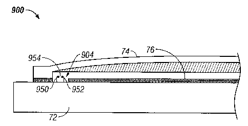
Figure 9B is a partial cross section view of a display device packaging
structure with an
exemplary water vapor sensor 904. The water vapor sensor 904 illustrated in
Figure 9B
comprises two conductive members 950, 952 with an air gap 954 between the
conductive
members 950, 952. In the absence of water vapor, the resistance between the
conductive
members 950, 952 is substantially infinite. However, as the level of water
vapor in the display
packaging structure increases, thereby increasing the amount of water vapor
between the
conductive members 950, 952, the resistance between the conductive members
950, 952
decreases corresponding to the amount of water vapor present. The sensor
circuit 906 may be
1 S outside the enclosed packaging structure or within the packaging
structure. As will be
appreciated by those skilled in the art, the water vapor sensor described is
exemplary in nature
and other sensors are within the scope of the invention.
In another embodiment of a MEMS display device with an end-of life phenomenon,
the
operational lifetime of the display is predetermined according to properties
of the device and
packaging. The operational lifetime of the display may be determined based on
the maximum
water vapor presence at which the movable layer of a MEMS element will still
be separable from
its corresponding fixed layer without continued activation. In one embodiment,
the operational
lifetime of the display may be determined based at least in part on the
absorption capacity of a
desiccant included in the display packaging structure and expected permeation
rate of water
vapor into the packaging structure. In one embodiment, data representing the
operational lifetime
of a display is stored in a memory coupled to a processor, such as the
processor 21 of Figure 2,
wherein the processor is configured to determine when the predetermined
lifetime has expired.
In response to determining the expiration of the display's lifetime, the
processor is configured to
coordinate activation of the display such that a predefined image is displayed
to the user. In one
embodiment, the processor is further configured to determine when the current
life of the MEMS
display is within a predefined range of the predetermined lifetime, and
coordinate activation of
the display so as to display a warning image in response to determining that
the current life the
MEMS display is within the predefined range of the predetermined lifetime.
In yet another embodiment of a MEMS display device with an end-of life
phenomenon,
individual MEMS elements of the MEMS display have differing cavity heights.
The depicted
portion of the MEMS array in Figure 10 includes five adjacent MEMS elements
1002a-e. The
-IS-
CA 02520950 2005-09-23
MEMS elements 1002a-a comprise a mechanical or movable layer 1004 and an
electrically
conductive fixed layer 1006, wherein the movable layer 1004 is positioned on
top of posts 1008a-
f and the conductive fixed layer 1006 is formed on a substrate 1009. The
movable layer 1004 and
fixed layer 1006 form cavities lOlOa-a for each respective MEMS element 1002a-
e. As
illustrated in Figure 10, the posts 1008a-f have differing heights, and
thereby the respective
cavities lOlOa-a for each MEMS element 1002a-a have a different height. For
the MEMS
elements 1002b-d with a reduced cavity height, the mechanical or movable layer
1004 will
remain adhered to the fixed layer 1006 in the presence of less water vapor
than the MEMS
elements 1002a, a with a greater cavity height. Thus, an image will be
displayed on the MEMS
display according to the MEMS elements with a reduced cavity height in the
presence of
sufficient water vapor.
In an additional embodiment of a MEMS display device with an end-of life
phenomenon,
the display device packaging structure includes a desiccant with varied
degrees of absorbent
capacity across its surface. Figure 11 is a cross section view of one
exemplary implementation of
a display device package structure with a varied desiccant 80. Elements
similar to those
illustrated in Figure 7 and described in reference thereto are labeled with
corresponding reference
numerals. As illustrated in Figure 11, the desiccant 80 is applied to the
backplane 74 of the
packaging structure, wherein the desiccant 80 includes preselected areas 1102
having
substantially less desiccant 80 than other unselected areas. MEMS elements of
the display device
76 located proximate to the preselected areas 1102 will remain in a
permanently active state,
wherein the movable layer adheres to the fixed layer, in the presence of
sufficient water vapor in
the packaging structure due to the reduced desiccant 80, whereas the MEMS
elements proximate
the unselected areas of the desiccant 80 will remain operational because the
desiccant 80 has
retained the water vapor in those areas. Accordingly, a predefined image will
be displayed on the
MEMS display device 76 according to the MEMS elements in the preselected areas
1102. As
will be appreciated by those skilled in the art, the preselected areas of the
desiccant may include
no desiccant, or desiccant with a reduced absorption capacity in comparison to
the desiccant in
the unselected areas.
In another embodiment of a MEMS display device configured for an end-of life
phenomenon, a user can apply a temperature differential to a surface of the
display package, such
as extreme cold or heat, thereby causing movement of water vapor molecules in
the display
device packaging structure proximate areas where the temperature differential
is applied. The
temperature differential can be applied, for example, with a cold or hot
tipped stylus to the
surface of the display, wherein an image is displayed according to the areas
where the stylus is
applied. The generated effect is similar to that of novelty devices wherein a
magnetic stylus is
applied to a surface of a screen containing metallic filaments, such that the
metallic filaments are
-16-
CA 02520950 2005-09-23
attracted to the surface of the screen according to the application of the
magnetic stylus to display
an image. Thus, when a hot-tipped stylus is used, the MEMS elements that are
contacted are
released to a reflective or white state, and when a cold-tipped stylus is
used, the MEMS elements
that are contacted are stuck in an activated or black state.
One embodiment of a method of activating an end-of life phenomenon comprises
applying extreme cold or reduced temperature to selective areas of a surface
of the display, using
a cold or cold-tipped stylus for example. Figure 12A is an exemplary
illustration of a MEMS
display 1200 comprising a plurality of MEMS elements 1202, wherein a reduced
temperature has
been applied to selective areas 1204. Application of the reduced temperature
generates
condensation of water vapor molecules present in the MEMS display device
package at the
selective areas 1204 where the reduced temperature is applied. In certain
embodiments, the
amount of water vapor present in the MEMS display device package is sufficient
to further
actuate or maintain MEMS elements in an activated position at the selected
areas, such that an
image is displayed at the selected areas 1204 as illustrated in Figure 12A.
The method may further comprise activating the display to actuate the movable
layers of
a plurality of MEMS elements, and then de-activating the display to move the
movable layers of a
plurality of MEMS elements to a released state. Due to the condensation of
water vapor
molecules at the selected areas 1204, the MEMS elements in the selected areas
1204 will remain
in an actuated position without continued activation, thereby displaying an
image on the MEMS
display at the selected areas, as illustrated in Figure 12A for example. In
some embodiments, the
display may be further activated to clear the display of the image.
Another embodiment of a method of activating an end-of life phenomenon
comprises
applying heat or increased temperature to selective areas of a surface of the
display, using a hot
or hot-tipped stylus for example. Application of increased temperature to the
display generates
evaporation of water vapor molecules present in the MEMS display device
package at the
selected areas where the increased temperature is applied. Figure 12B is an
exemplary
illustration of a MEMS display 1220 comprising a plurality of MEMS elements
1222, wherein an
increased temperature has been applied to selective areas 1224 of the display
which has reached
the end of its operational lifetime. Tn one embodiment, the MEMS display
device has already
reached the end of its operational lifetime due to the presence of sufficient
water vapor in the
MEMS display device package, wherein a plurality of the MEMS elements of the
display remain
in an activated or actuated state without continued activation. In certain
embodiments,
substantially all of the MEMS elements are in an activated state without
continued activation, as
illustrated in Figure 12B. When a user applies an increased temperature
difference to the
selective areas 1224 of the display 1220, the MEMS elements at the selected
areas 1224 move to
a released state as the water vapor retaining the movable membrane in the
activated state
_17_
CA 02520950 2005-09-23
evaporates in response to the increased temperature application. As
illustrated in Figure 12B, the
MEMS elements at the selected areas 1224 are in a released state while MEMS
elements in
unselected areas remain in an activated state, thereby displaying an image
according to the
selected areas 1224.
S In certain embodiments, the method may include detecting a predefined level
of water
vapor within the MEMS display device package and notifying a user that the
display is near the
end of its operable lifetime. The user may then apply the reduced temperature
to display an
image at selected areas of the display as discussed above. Alternatively, in
response to
notification that the display is near the end of its operable lifetime, the
user may activate the
display when sufficient water vapor is present in the display package such
that a plurality of
MEMS elements remain in an activated position without continued activation.
The user may then
apply an increased temperature to selective areas of the display such that the
MEMS elements at
the selected areas are "released" to a released state, thereby displaying an
image on the display
according to the selected areas. In additional embodiments, a user may
intentionally contact the
MEMS display with water vapor as discussed above with respect to other
embodiments of the
invention. In addition, the method may further comprise activation of the
display to clear the
image.
As discussed above, a MEMS display device has a significant tolerance for
water vapor,
wherein the display will continue to operate in the presence of a significant
level of water vapor
ZO as compared to other display devices such as OLED's. It is generally known
that OLED displays
have significant environmental constraints on the amount of water and oxygen
present both
during assembly and inside the final package display. In contrast, embodiments
of MEMS
displays do not mandate an inert, vacuum or dry environment during assembly or
operation.
Thus, MEMS displays tolerate exposure to significant levels of water vapor
before reaching a
non-operational state, whereas an OLED display device has substantially zero
tolerance for the
presence of water vapor and the entirety of an OLED display will be non-
operational once
exposed to a small level of water vapor. The ability of MEMS display elements
to tolerate the
presence of water vapor and remain operational allows for the implementation
of the above-
described embodiments of display devices with end-of life phenomena.
Figures 13A and 13B are system block diagrams illustrating an embodiment of a
display
device 2040. The display device 2040 can be, for example, a cellular or mobile
telephone.
However, the same components of display device 2040 or slight variations
thereof are also
illustrative of various types of display devices such as televisions and
portable media players.
The display device 2040 includes a housing 2041, a display 2030, an antenna
2043, a
speaker 2045, an input device 2048, and a microphone 2046. The housing 2041 is
generally
formed from any of a variety of manufacturing processes as are well known to
those of skill in
-18-
CA 02520950 2005-09-23
the art, including injection molding, and vacuum forming. In addition, the
housing 2041 may be
made from any of a variety of materials, including but not limited to plastic,
metal, glass, rubber,
and ceramic, or a combination thereof. In one embodiment the housing 2041
includes removable
portions (not shown) that may be interchanged with other removable portions of
different color,
or containing different logos, pictures, or symbols.
The display 2030 of exemplary display device 2040 may be any of a variety of
displays,
including a bi-stable display, as described herein. In other embodiments, the
display 2030
includes a flat-panel display, such as plasma, EL, OLED, STN LCD, or TFT LCD
as described
above, or a non-flat-panel display, such as a CRT or other tube device, as is
well known to those
of skill in the art. However, for purposes of describing the present
embodiment, the display 2030
includes an interferometric modulator display, as described herein.
The components of one embodiment of exemplary display device 2040 are
schematically
illustrated in Figure 13B. The illustrated exemplary display device 2040
includes a housing 2041
and can include additional components at least partially enclosed therein. For
example, in one
embodiment, the exemplary display device 2040 includes a network interface
2027 that includes
an antenna 2043 which is coupled to a transceiver 2047. The transceiver 2047
is connected to the
processor 2021, which is connected to conditioning hardware 2052. The
conditioning hardware
2052 may be configured to condition a signal (e.g. filter a signal). The
conditioning hardware
2052, is connected to a speaker 2045 and a microphone 2046. The processor 2021
is also
connected to an input device 2048 and a driver controller 2029. The driver
controller 2029 is
coupled to a frame buffer 2028 and to the array driver 2022, which in turn is
coupled to a display
array 2030. A power supply 2050 provides power to all components as required
by the particular
exemplary display device 2040 design.
The network interface 2027 includes the antenna 2043 and the transceiver 2047
so that
the exemplary display device 2040 can communicate with one or more devices
over a network.
1n one embodiment the network interface 2027 may also have some processing
capabilities to
relieve requirements of the processor 2021. The antenna 2043 is any antenna
known to those of
skill in the art for transmitting and receiving signals. In one embodiment,
the antenna transmits
and receives RF signals according to the IEEE 802.11 standard, including IEEE
802.11(a), (b), or
(g). In another embodiment, the antenna transmits and receives RF signals
according to the
BLUETOOTH standard. In the case of a cellular telephone, the antenna is
designed to receive
CDMA, GSM, AMPS or other known signals that are used to communicate within a
wireless cell
phone network. The transceiver 2047 pre-processes the signals received from
the antenna 2043
so that they may be received by and further manipulated by the processor 2021.
The transceiver
2047 also processes signals received from the processor 2021 so that they may
be transmitted
from the exemplary display device 2040 via the antenna 2043.
-19-
CA 02520950 2005-09-23
In an alternative embodiment, the transceiver 2047 can be replaced by a
receiver. In yet
another alternative embodiment, network interface 2027 can be replaced by an
image source,
which can store or generate image data to be sent to the processor 2021. For
example, the image
source can be a digital video disc (DVD) or a hard-disc drive that contains
image data, or a
software module that generates image data.
Processor 2021 generally controls the overall operation of the exemplary
display device
2040. The processor 2021 receives data, such as compressed image data from the
network
interface 2027 or an image source, and processes the data into raw image data
or into a format
that is readily processed into raw image data. The processor 2021 then sends
the processed data
to the driver controller 2029 or to frame buffer 2028 for storage. Raw data
typically refers to the
information that identifies the image characteristics at each location within
an image. For
example, such image characteristics can include color, saturation, and gray-
scale level.
In one embodiment, the processor 2021 includes a microcontroller, CPU, or
logic unit to
control operation of the exemplary display device 2040. Conditioning hardware
2052 generally
includes amplifiers and filters for transmitting signals to the speaker 2045,
and for receiving
signals from the microphone 2046. Conditioning hardware 2052 may be discrete
components
within the exemplary display device 2040, or may be incorporated within the
processor 2021 or
other components.
The driver controller 2029 takes the raw image data generated by the processor
2021
either directly from the processor 2021 or from the frame buffer 2028 and
reformats the raw
image data appropriately for high speed transmission to the array driver 2022.
Specifically, the
driver controller 2029 reformats the raw image data into a data flow having a
raster-like format,
such that it has a time order suitable for scanning across the display array
2030. Then the driver
controller 2029 sends the formatted information to the array driver 2022.
Although a driver
controller 2029, such as a LCD controller, is often associated with the system
processor 2021 as a
stand-alone Integrated Circuit (1C), such controllers may be implemented in
many ways. They
may ~ be embedded in the processor 2021 as hardware, embedded in the processor
2021 as
software, or fully integrated in hardware with the array driver 2022.
Typically, the array driver 2022 receives the formatted information from the
driver
controller 2029 and reformats the video data into a parallel set of waveforms
that are applied
many times per second to the hundreds and sometimes thousands of leads coming
from the
display's x-y matrix of pixels.
In one embodiment, the driver controller 2029, array driver 2022, and display
array 2030
are appropriate for any of the types of displays described herein. For
example, in one
embodiment, driver controller 2029 is a conventional display controller or a
bi-stable display
controller (e.g., an interferometric modulator controller). In another
embodiment, array driver
-20-
CA 02520950 2005-09-23
2022 is a conventional driver or a bi-stable display driver (e.g., an
interferometric modulator
display). In one embodiment, a driver controller 2029 is integrated with the
array driver 2022.
Such an embodiment is common in highly integrated systems such as cellular
phones, watches,
and other small area displays. In yet another embodiment, display array 2030
is a typical display
array or a bi-stable display array (e. g., a display including an array of
interferometric
modulators).
The input device 2048 allows a user to control the operation of the exemplary
display
device 2040. In one embodiment, input device 2048 includes a keypad, such as a
QWERTY
keyboard or a telephone keypad, a button, a switch, a touch-sensitive screen,
a pressure- or heat-
sensitive membrane. In one embodiment, the microphone 2046 is an input device
for the
exemplary display device 2040. When the microphone 2046 is used to input data
to the device,
voice commands may be provided by a user for controlling operations of the
exemplary display
device 2040.
Power supply 2050 can include a variety of energy storage devices as are well
known in
I 5 the art. For example, in one embodiment, power supply 2050 is a
rechargeable battery, such as a
nickel-cadmium battery or a lithium ion battery. In another embodiment, power
supply 2050 is a
renewable energy source, a capacitor, or a solar cell, including a plastic
solar cell, and solar-cell
paint. In another embodiment, power supply 2050 is configured to receive power
from a wall
outlet.
In some implementations control programmability resides, as described above,
in a driver
controller which can be located in several places in the electronic display
system. In some cases
control programmability resides in the array driver 2022. Those of skill in
the art will recognize
that the above-described optimization may be implemented in any number of
hardware and/or
software components and in various configurations.
The foregoing description details certain embodiments of the invention. It
will be
appreciated, however, that no matter how detailed the foregoing appears in
text, the invention can
be practiced in many ways. As is also stated above, it should be noted that
the use of particular
terminology when describing certain features or aspects of the invention
should not be taken to
imply that the terminology is being re-defined herein to be restricted to
including any specific
characteristics of the features or aspects of the invention with which that
terminology is
associated. The scope of the invention should therefore be construed in
accordance with the
appended claims and any equivalents thereof.
-21-