Note: Descriptions are shown in the official language in which they were submitted.
CA 02521408 2005-09-28
DUAL POWER SUPPLY SWITCHING CIRCUITRY FOR USE IN A CLOSED
SYSTEM
BACKGROUND OF THE INVENTION
Field of the Invention
The present invention is directed to a closed system such as a transcutaneous
energy
transfer (TET) system and, in particular, to a dual power supply switching
system for a TEl
system wherein powering of an implantable medical device and its associated
components is
switched, during communication from the external device to the implant,
between an internal
power source of the implantable medical device and an external RF power source
produced
by the external device.
Description of Related Art
In a variety of scientific, industrial, and medically related applications, it
may be
desirable to transfer energy or power (energy per unit time) across some type
of boundary.
For example, one or more devices that require power (e.g., electrical,
mechanical, optical, and
acoustic devices) may be located within the confines of a closed system, or
"body," in which
it may be difficult and/or undesirable to also include a substantial and/or
long term source of
power. The closed system or body may be delimited by various types of physical
boundaries,
and the system internal to the boundary may be living or inanimate, may
perform a variety of
functions, and may have a variety of operational and physical requirements
and/or constraints.
In some cases, such requirements and constraints may make the implementation
of a
substantial and/or long term "internal" power source for internally located
devices
problematic.
CA 02521408 2005-09-28
In some closed systems, repeated entry into the system may be undesirable for
a '
variety of reasons. In other closed systems, significant internal power
requirements and a
limited internal space may prohibit the implementation of a suitably sized
internal power
source. In yet other systems, contamination and/or security issues may pose
particular
One common example of a closed system is the human body. In some medically
Accordingly, in some medical implant applications, "transcutaneous energy
transfer"
(TET) devices are employed to transfer energy from outside the body to inside
the body, to
provide power to one or more implanted prostheses or devices from an external
power source.
In a system employing an implantable medical device and external control unit
each of
the implantable medical device and external control unit preferably has its
own power source,
e.g., a battery, for powering its associated circuitry and its associated
components. The
implantable medical device battery, regardless of whether primary/non-
rechargeable or
30 secondary/rechargeable, has a limited lifespan and a predetermined amount
of energy or
power before having to be replaced or recharged.
2
CA 02521408 2005-09-28
It is therefore desirable to develop and an improved TET system having
circuitry for
optimally switching from an internal power source to an external RF power
source so as to
reduce the energy consumed from the internal power source associated with the
implant.
Summary of the Invention
The present invention is directed to TET system that includes circuitry for
optimally
switching from an internal power source to an external RF power source.
The present invention is directed to TET system that minimizes power
consumption of
the implantable medical device power source.
One aspect of the invention relates to a closed system such as a TET system
having
dual power supply switching circuitry. The system includes an internal device
disposed
interior of a boundary and powered by an internal power source. Disposed
separated from
the internal device and exterior to the boundary is an external device. The
external device is
in telemetric communication with the internal device and generates an external
RF energy
source during telemetric communication with the internal device. Power
switching circuitry
is used to switch from the internal power source to the external RF energy
source during
communication from the external device to the internal device when power
supplied by the
external RF energy source exceeds that required for powering the internal
device.
Yet another aspect of the present invention is directed to a method for
operating the
dual power supply switching circuitry in the system described above.
Specifically, the
method is realized by generating during communication of the external device
with the
internal device an external RF energy source. During communication from the
external
device to the internal device when power supplied by the external RF energy
source exceeds
that required for powering the internal device, powering of the internal
device is switched
from the internal power source to the external RF energy source using power
switching
circuitry.
Brief Description of the Drawing
The foregoing and other features of the present invention will be more readily
apparent from the following detailed description and drawings of illustrative
embodiments of
3
CA 02521408 2005-09-28
the invention wherein like reference numbers refer to similar elements
throughout the several
views and in which:
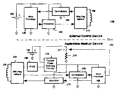
Figure 1 is a schematic diagram of an exemplary TET system in accordance with
the
present invention including an external device in telemetric communication
with an
implantable medical device, wherein the implantable medical device employs
passive power
switching circuitry;
Figure 2a is a schematic diagram of exemplary passive power switching
circuitry in
Figure 1;
Figure 2b is an exemplary flow diagram of the passive power switching
circuitry of
Figure 2a;
Figure 3a is a schematic diagram of an exemplary implantable medical device
employing active power switching circuitry for use in a TET system; and
Figure 3b is an exemplary flow diagram of the active power switching circuitry
of
Figure 3a.
Detailed Description of the Invention
The present invention is directed to an energy efficient closed system such as
a TET
system that includes a first internal electronic device in telemetric
communication with and
separated by a physical boundary by a second external electronic device,
wherein each
electronic device has its own power source (e.g., battery). By way of example,
the TET
system and method in accordance with the present invention is shown in Figure
1 for an
implantable drug infusion pump in telemetric communication with an external
device, e.g., a
control unit or PC. It is to be understood, however, that the present
invention may be used for
other implantable medical devices or other electronic devices not related to
the medical field.
The present invention is suitable for any closed system comprising two
electronic devices that
communicate via telemetric link, wherein the energy used to power the internal
device is
optimally switched from an internal power source to an external RF source
produced by the
external device during communication with the internal device.
The exemplary TET system shown Figure 1 comprises an external device 100
(e.g., a
control unit) in telemetric communication with an implantable medical device
105 (e.g., an
implantable drug infusion pump). External device 100 includes a primary coil
110 connected
to a tuned matching network or circuit 115. A demodulator 150 is connected to
the matching
4
CA 02521408 2005-09-28
network 115 and demodulates the data signal from the received carrier signal.
In Win, the
demodulator 150 is electrically connected by a microprocessor or controller
140. A
transmitter 145 is connected between the microprocessor 140 and matching
network 115. All
components and circuitry associated with the external device 100 are powered
by a primary
power source 125. In a preferred embodiment, the power source 125 for powering
the
external device and its associated circuitry and components is a
secondary/rechargeable
battery, most preferably a smart rechargeable battery.
The implantable medical device 105 has an associated secondary coil 120
connected
to tuned a matching network or circuit 155. A demodulator 160 is connected to
the matching
network 155 for extracting the data signal from the received carrier signal.
Microprocessor
135 is, in turn, connected to the demodulator 160. Electrically connected
between the
microprocessor 135 and matching network 155 is a modulator 170 for modulating
the signal
prior to transmission to the external device 100. A secondary or internal
power source 130
provides power to all the components and circuitry associated with the
implantable medical
device. Sometimes the implantable medical device 105 such as an implantable
drug infusion
pump remains continuously active at all times to maintain operation of the
components and
circuitry associated therewith. In such applications, the secondary power
source 130 is
preferably a primary/non-rechargeable battery.
Heretofore, the components and circuitry of the implantable medical device 105
have
been powered exclusively by its associated internal power source 130, e.g.,
battery. During
telemetric communication from the external device 100 to the implantable
medical device 105
an RF field is generated. This external RF energy source may be used as an
alternative source
for providing power needed by the implantable medical device 105 and
associated circuitry to
operate which would otherwise be drawn from the internal battery 130
associated with the
implantable medical device. Accordingly, the implantable medical device 105 in
accordance
with the present invention has been designed to include a high frequency-to-DC
converter
(HF/DC) 180 and passive power switching circuitry 175 to optimally switch
powering of the
implantable medical device 105 and its associated components and circuitry
from the internal
power source 130 to the external RF energy source. Switching between power
sources should
preferably be instantaneous, automatic and relatively smooth.
Figures 2a & 2b represent schematic and flow diagrams, respectively, of
exemplary
passive power switching circuitry 175 of Figure 1 using diodes. By way of
example, power
CA 02521408 2005-09-28
switching circuitry 175 is used to switch between an internal battery source
130 associated
with the implantable medical device 105 and an external RF energy source
emitted by an
external device 100 during communication with the implantable medical device.
In Figure 2a,
demodulator 160, microprocessor 135 and modulator 170 are generically
represented by
implant electronics 200. Despite not being shown, the implantable medical
device may
include additional components as part of the implant electronics 200 depending
on the
particular functionality of the implant device. For example, an implantable
drug infusion
pump may include circuitry for controlling the opening and closing of the
valve to the
reservoir in which the medication is stored.
A first diode 205 is electrically connected between the voltage supply line
(Vsupply)
and the RF voltage (Vr-f), while a second diode 210 is connected between the
voltage supply
line (Vsupply) and the battery voltage (Vbattery). A capacitor 220 is
connected to the voltage
supply line (Vsupply) and serves as the stopgap energy supplier during
switching of the
power supply between Vbattery and Vrf to prevent any interruption in
communication.
Typically, the components when powered by the internal battery utilize
substantially
all the energy in the battery. By way of example, the implantable components
may require a
minimum of approximately 1.8 V and a maximum of approximately 3.6 V to
operate, while
the battery voltage is selected to be approximately 2.8 V when fully charged
and drops to
approximately 1.8 V towards the end of life of the battery. However, a forward
voltage drop
is experienced across the diode. This drop in voltage will reduce the full
range of the battery
that is able to power the components. In designing the power switching
circuitry it is
desirable to select a diode such as a Schottky diode having a relatively low
voltage drop,
preferably approximately 0.2 V to approximately 0.4 V. Due to the forward
voltage drop
across the diode the components will operate between approximately 2.8 V and
approximately
2.1 V (minimum working voltage of approximately 1.8 V + diode forward voltage
drop (e.g.,
approximately 0.3 V)). Once the battery voltage falls below approximately 2.1
V (minimum
working voltage of approximately 1.8 V + the forward voltage drop (e.g.,
approximately 0.3
V)) the battery will not be able to supply the voltage needed to operate the
components. Thus,
the full battery range capable of powering the components is reduced by the
forward voltage
drop across the diode.
In operation, during communication of the external device 100 with the
implantable
medical device 105, if the power supplied by the external RF energy source
exceeds that
6
CA 02521408 2005-09-28
required to energize the implantable medical device and its associated
components, then the
second diode 210 is reverse biased and all power is drawn from the external RF
power source.
When power is drawn from the external RF energy source, a backward or reverse
leakage
current is exhibited in diode 210 which is detrimental to the battery 130. To
circumvent this
potentially damaging effect on the battery, a leakage current path is created
via a switch 217
connected in series to a resistor 215 whose resistance is lower than that of
the battery 130. In
the presence of an external RF voltage, switch 217 is closed so that,the
leakage current flows
through the resistor 215 rather than the battery 130.
On the other hand, whenever there is no RF communication or the RF energy
emitted
during communication from the external device 100 to the implantable medical
device 105 is
less than or equal to that required to energize the implantable medical device
and its
associated components, the first diode 205 is reverse biased and all
components in the
implantable medical device draw power from the battery 130. Thus, switching of
the power
source used to energize the implantable medical device and its associated
components from
the battery to the external RF energy source emitted by the external device
during
communication with the implant will occur only when the power supplied by the
emitted RF
field exceeds that required to energize the implantable medical device and its
associated
components. Substantially all the battery potential is typically consumed by
the components
and associated circuitry of the implantable medical device when powered by the
battery 130.
Under such circumstances, switching from the internal power source 130 to the
external 12F
power source will take place only when the external RF voltage potential
exceeds the battery
voltage.
Alternatively, the implantable device may employ active power switching
circuitry.
Figures 3a & 3b show a schematic diagram and flow diagram, respectively, of
exemplary
active power switching circuitry 190 using an analog switch. In Figure 3a,
implant
electronics block 200 generically represents the modulator 170, demodulator
160,
microprocessor 135 and any other circuitry associated with the specific
functionality of the
implant that is not otherwise specifically shown. An analog switch 305 is
electrically
connected to the RF voltage supply line (Vrf), the battery voltage supply line
(Vbattery), and
the voltage supply line (Vsupply). Preferably, the analog switch 305 is chosen
so as to satisfy
the following requirements: relatively low ON resistance; relatively high OFF
resistance;
relatively low leakage current; relatively low capacitance. In order to bias
the internal
7
CA 02521408 2005-09-28
circuitry, analog switch 305 is continuously powered by the battery 130.
Accordingly, as
depicted in the flow diagram of Figure 3b, the battery supply line (Vbattery)
is electrically
connected to the normally closed (NC) input of the analog switch 305, while
the RF 'voltage
supply line (Vrf) is connected to the normally open (NO) input of analog
switch 305. The
additional drain on the battery in having to continuously power the analog
switch increases
the overall average current consumption of the components of the implantable
medical device.
During RF communication from the external device 100 to the implantable
medical
device 105, the microprocessor 135 in the implantable medical device
determines whether the
power supplied by the external RF energy source exceeds that required to
energize the
implantable medical device and its associated components. If so,
microprocessor 135 asserts
an enable signal used to trigger analog switch 305 to switch from the internal
power source
130 to the external RF energy source. In the absence of RF communication from
the external
device to the implantable medical device the enable signal from the
microprocessor 135 is
disabled and the capacitor 220 connected to the Vsupply line is charged
automatically from
the battery 130. As discussed above, capacitor 220 serves as the stopgap
energy supplier
while switching from the internal battery to the external RF energy source
supplying power to
the implantable medical device and its associated components.
Other active components may be employed instead of an analog switch. The use
of
diodes in accordance with the first embodiment of the invention, however, is
preferred over
that of the second embodiment using an analog switch due to the increased
battery power
consumption and larger area footprint on the circuit board when employing an
analog switch.
Yet still another disadvantage associated with use of an analog switch is that
it requires an
external logic element (e.g., a microprocessor or controller) for sensing the
voltage and
controlling the switch. In contrast, the diode configuration is totally
passive and not triggered
by a microprocessor.
Thus, while there have been shown, described, and pointed out fundamental
novel
features of the invention as applied to a preferred embodiment thereof, it
will be understood
that various omissions, substitutions, and changes in the form and details of
the devices
illustrated, and in their operation, may be made by those skilled in the art
without departing
from the spirit and scope of the invention. For example, it is expressly
intended that all
combinations of those elements and/or steps that perform substantially the
same function, in
substantially the same way, to achieve the same results be within the scope of
the invention.
8
CA 02521408 2013-09-20
Substitutions of elements from one described embodiment to another are also
fully intended
and contemplated. It is also to be understood that the drawings are not
necessarily drawn to
scale, but that they are merely conceptual in nature. It is the intention,
therefore, to be limited
only as indicated by the scope of the claims appended hereto.
9