Note: Descriptions are shown in the official language in which they were submitted.
CA 02523105 2005-10-21
WO 2004/095519 PCT/US2004/012634
METHOD AND SYSTEM FOR COUPLING WAVEGUIDES
Related Application
(0001] This applicafion claims priority of United States Patent
Application serial No. 60/464,763, entitled "MULTIPLE LAYER
WAVEGUIDE STRUCTURES FOR A-SI BASED PHOTONIC INTEGRATED
CIRCUITS, SLOPED COUPLING JOINT IN A-SI BASED PHOTONIC
INTEGRATED CIRCUITS AND CIRCUITS INCLUDING SAME", filed April
23, 2003, the entire disclosure of which is hereby incorporated by reference
as if being set forth in its entirety herein.
Field of Invention
[0002] The present invention relates to waveguide coupling
techniques, such as those used in connection with photonic integrated
circuits.
Background of the Invention
(0003] Widespread development and proliferation of Photonic
Integrated Circuits (PICs) including active components, such as III-V
semiconductor photonic devices like lasers and modulators, and passive
components, such as passive waveguides, are believed highly desirable.
Such circuits and devices may be monolithic in nature. One challenge in
developing such PICs lies in integrating both active and passive
CA 02523105 2005-10-21
WO 2004/095519 PCT/US2004/012634
components, and operationally coupling them to one-another. This may
result from using different materials, having different indices of refraction
for
example, in active and passive components.
[0004] One approach may include butt coupling the active and
passive devices together. However, this may conventionally require precise
alignment of the active and passive devices to achieve desired coupling
efficiencies.
(0005] Accordingly, a method and system that provides for improved
coupling of active and passive photonic devices together, such as in a PIC
by way of non-limiting example only, is believed desirable.
Summary of the Invention
(0006] A method for photonically coupling to at least one active
photonic device structure formed on a substrate, the method including:
etching the active device structure with a high selectivity towards a
crystallographic plane to form a sloped terminice with respect to the
substrate; and, depositing at least one waveguide over the etched terminice
and at least a portion of the substrate; wherein, the waveguide is
photonically coupled to the etched active device structure to provide
photonic interconnectivity for the etched active device structure.
Brief Description of the Figures
2
CA 02523105 2005-10-21
WO 2004/095519 PCT/US2004/012634
(0007] Understanding of the present invention will be facilitated by
consideration of the following detailed description of the preferred
embodiments taken in conjunction with the accompanying drawings, in
which like numerals refer to like parts, and:
(0008] Figure 1 illustrates three and two layer waveguide coupling
joints according to aspects of the present invention;
(0009] Figure 2 illustrates vertical (illustration a) and sloped
(illustration b) active / passive junctions or interfaces according to aspects
of
the present invention;
(0010] Figure 3 illustrates an active / passive junction at various
processing steps according to an aspect of the present invention;
(0011] Figure 4 illustrates SEM micrographs of the semiconductor
step edge produced by a non-selective wet chemical etch and a flat area in
a channel, according to an aspect of the present invention;
(0012] Figure 5 illustrates an SEM image of a coupling joint fabricated
using a selective wet etch according to an aspect of the present invention;
(0013] Figure 6 illustrates an SEM image of a coupling joint fabricated
using a combination of selective and non-selective wet etches according to
an aspect of the present invention;
(0014] Figure 7 illustrates a coupling joint profile from a wet and dry
etch sequence, according to an aspect of the present invention; and,
3
CA 02523105 2005-10-21
WO 2004/095519 PCT/US2004/012634
[0015] Figure 8 illustrates a coupling joint of a device after an a-Si
deposition and etch, according to an aspect of the present invention.
Detailed Description of the Invention
[0016] It is to be understood that the figures and descriptions of the
present invention have been simplified to illustrate elements that are
relevant for a clear understanding of the present invention, while
eliminating,
for purposes of clarity, many other elements found in typical PICS, active
devices, passive devices and coupling methods. Those of ordinary skill in
the art will recognize that other elements may be desirable in implementing
the present invention. However, because such elements are well known in
the art, and because they do not facilitate a better understanding of the
present invention, a discussion of such elements is not provided herein.
The disclosure herein is directed to all such variations and modifications
known to those skilled in the art.
[0017] According to an aspect of the present invention, amorphous
silicon (a-Si) based waveguides may be used for Photonic Integrated Circuit
(PIC) integration. A two layer structure may be used to reduce losses at
active/passive device coupling joints and may be simpler to manufacture
than a three layer structure.
[0018] Referring now to Figure 1, there are shown a three layer
coupling system 100 for an active device 110 and passive waveguide 120
4
CA 02523105 2005-10-21
WO 2004/095519 PCT/US2004/012634
(illustration a), and a two layer coupling system 200 for an active device 110
and passive waveguide 120 (illustration b).
(0019] Active device 110 may take, the form of any suitable active
device, such as a bulk semiconductor, quantum well or quantum dot based
device, by way of non-limiting example only. Such a device may be
characterized as having long wavelength operational characteristics, for
example. Such a device may incorporate III-V semiconductor materials for
example. Such a device may incorporate GaAs or InGaAs materials, for
example. Such a device may form a laser, or portion thereof, a modulator,
or portion thereof, or a gain section for a larger system, all by way of non-
limiting example only. Device 110 may have a core 115, as will be readily
understood by those possessing an ordinary skill in the pertinent arts.
Device 110 may have one or more terminices 117 that are desirable to have
one or more waveguides 120 operationally coupled to. Figure 1 illustrates a
single terminice 117 and waveguide 120 for purposes of illustration only.
[0020] According to an aspect of the present invention, waveguide
120 may include upper cladding layer 127 and an active layer 125.
According to an aspect of the present invention, waveguide 120 may
optionally include a lower cladding 123. According to an aspect of the
present invention, upper cladding 123, core 125, and lower cladding 127
may take the form of an a-Si based material such as a-SiNxHy (0<x<1.3,
0<y<0.3), a-SiCxHy (0<x<1, 0<y<0.3), or a-SiOxHy (0<x<1, 0<y<.3). The
desired refractive index for the upper cladding 123, core 125, and lower
CA 02523105 2005-10-21
WO 2004/095519 PCT/US2004/012634
cladding 127 may be achieved by adjusting the composition of the a-Si
based material. The upper and lower cladding layers may have an index of
refraction around 3.17. The core may have an index of refraction between
around 3.27 and around 3.32. Layers 127, 125 may be of any suitable
thickness, such as about 1 pm for layer 127, and about 0.3 pm for layer 125.
Layer 123, if present, may have any suitable thickness as well, such as
about 1 pm, by way of non-limiting example only.
[0021] Illustration (a) shows a three-layer passive waveguide 130
including layer 123, while illustration (b) shows a two-layer passive
waveguide 140 omitting layer 123. In either case, a suitable substrate, such
as an In-P substrate of suitable thickness, such as about 0.35 mm thick,
may be used. Such a substrate may have in index of refraction around 3.17,
for example. In the case of a 2-layer waveguide configuration, such as that
shown in illustration (b), one or more layers in common with active device
110 and/or the substrate may be used to at least partially clad or confine the
passive waveguide 140 core.
[0022] Active device 110 may be formed using conventional
methodologies. For example, device 110 may be formed by first depositing
a stack of quaternary layers upon a conventional InP substrate. The stack
may form the active layer of the device and include alternating 95 nm thick
InGaAs and InGaAsP layers. For example, five layers may be provided. A
635 nm thick InP spacing/blocking layer may then be deposited upon the
active layer. A 30 nm thick InGaAsP etch stop layer may then be deposited.
6
CA 02523105 2005-10-21
WO 2004/095519 PCT/US2004/012634
A 1300 nm InP layer may then be deposited. And, finally a 50nm thick
InGaAs cap may be deposited. Deposition, of the layers may be
accomplished in conventional manners, such as by using liquid or plasma
enhanced chemical vapor deposition, for example.
[0023] Waveguides 130, 140 may be positioned with respect to
device 110, such that the core 115, or active layers, of device 110 is
operationally coupled to the cores 125 of waveguides 130, 140, respectively.
[0024] For example, and with regard to illustration (a) of Figure 1, a
lower cladding 123 may have a suitable thickness for elevating core 125
above substrate 119 to a level substantially aligned with core 115. With
regard to illustration (b), one or more layers 146 common to and used to
form or support part of device 110 may be used analogously.
[0025] As will be understood by those possessing an ordinary skill in
the pertinent arts, waveguide 130 may present several disadvantages
compared to waveguide 140. First, the deposition of the amorphous silicon
material on the sidewalls of device 110, i.e., terminice 117, may prove more
difficult in the three-layer structure, since a layer of low-index material is
included between the active and passive low-index layers. Second, the
alignment of the passive and active waveguide cores may prove more
challenging in a three-layer scheme, since the thickness of the passive
bottom-cladding layer may be significantly more than alignment tolerances.
And third, the overall thickness of the amorphous silicon may be
7
CA 02523105 2005-10-21
WO 2004/095519 PCT/US2004/012634
considerably higher in the three-layer scheme, which can lead to more
peeling and/or cracking problems in the presence of a relatively small stress,
for example.
[0026] According to an aspect of the present invention, interfaces
between active and passive components of a PIC may have sloped regions.
Referring now also to Figure 2, there are shown vertical (illustration a) and
sloped (illustration b), active / passive junctions or interfaces 210, 220.
Sloped coupling joints, such as that shown in illustration (b), may reduce
residual interface reflection in a-Si waveguide based photonic integrated
circuits, thus improving device performance. A vertical junction, such as that
shown in illustration (a), may tend to produce more significant back
reflections for a given effective index mismatch between the active and
passive waveguides. This back reflection can result in significant
interference and losses, which can deteriorate the performance of optical
devices such as semiconductor optical amplifiers (SOA) and super
luminescence diodes (SLD), by way of non-limiting example only. This risk
may be at least partially mitigated by suppressing reflections using a sloped
active-passive junction, since the average change of index may be less in
such a structure and the back reflection is not directed at the waveguide.
The slope of the sloped junction may align with and be dependent upon a
crystallographic plane of material incorporated into the active device being
coupled to, for example.
8
CA 02523105 2005-10-21
WO 2004/095519 PCT/US2004/012634
[0027] Referring still to Figure 2, each of systems 210, 220 may be
based upon the two layer coupling structure 140 of Figure 1. More
particularly, each system 210, 220 may include a substrate 230. Substrate
230 may take the form of an approximately 0.35 mm thick InP substrate
having an index of refraction of about 3.17, for example. Each system 210,
220 may include an active device region 240 and passive waveguiding
region 250. Region 240 may be analogous to active device 110 of Figure 1,
while region 250 may be analogous to waveguide 140 of Figure 1.
Undesirable reflections due to interface region 260 may be reduced in the
sloped system 220 as compared to vertical system 210, due, at least in part,
to residual interface reflections associated with region 260 not being aligned
with a core 215 of active region 240 or core 225 of waveguide region 250.
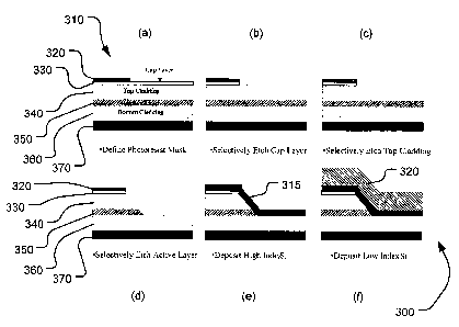
[0028] Referring now also to Figure 3, there is shown an active /
passive junction 300 at various processing steps (a) - (f) according to
aspects of the present invention. Junction 300 may take a form analogous
to that of system 220, for example.
[0029] According to an aspect of the present invention, a wet-based
chemical etching method may be used to produce active-passive junctions
with a high uniformity and reproducibility of the slope angle and total etch
depth. According to an aspect of the present invention, junction position and
shape may be defined using conventional photolithographic techniques.
This is illustrated in step (a), wherein system 310 is shown to include a
protective layer 320, cap layer 330, top cladding 340, active layers) 350,
9
CA 02523105 2005-10-21
WO 2004/095519 PCT/US2004/012634
bottom cladding 360 and substrate 370. In such a case, protective layer 320
may take the form of a photoresist mask for use in further processing, for
example. System 310 may define an active device, such as a laser, SOA or
SLD structure, for example.
[0030] Referring now also to step (b), cap layer 320 may then be
selectively removed, such as by etching for example. Referring now also to
step (c), top cladding layer 330 may then be etched with a high selectivity
towards a crystallographic plane. This may serve to provide a reproducible
slope while etch depth uniformity is also ensured by the active layer
providing etch stop functionality. Active layers) 340 may then be removed
selectively, again using conventional methodologies for example, as is
illustrated in step (d). As is shown in step (e), a high-index amorphous
silicon, which serves as waveguiding core 315, may then be deposited onto
the etched system 310. It may be noted that the slope may also serve to
reduce void formation at the corner of the active material. Finally, as is
shown in step (f), a low-index amorphous silicon, which forms top cladding
layer 320 of the passive waveguide, may be deposited in a conventional
manner, for example.
[0031] In general, and by way of non-limiting example only, several
methods for forming a sloped coupling joint are presented. A nominal 1550
nm emitting wavelength wafer that includes a 5-quantum well quaternary
stack of 95 nm thick layers were considered. Sections of the wafer were
defined with 200 micron openings on 800 micron spacing (mesas) and 400
CA 02523105 2005-10-21
WO 2004/095519 PCT/US2004/012634
micron openings on 600 micron spacing using photolithography. Several
etching experiments were performed on these wafer sections to fabricate a
deep groove defined in the resist openings through the laser active layer.
These grooves were subsequently used for amorphous silicon waveguide
deposition.
[0032] According to an aspect of the present invention, a wet
chemical etching of the grooves with a non-selective bromine/acetic acid
etch may be used. This etch may have substantially no selectivity to the
various layers of the active device structure, such that it does not stop at
different chemical compositions in the structure, for example. Referring
now also to Figure 4, there are shown SEM micrographs of the etched edge
surface with a sloped profile (a) and the flat area in the channel (b). The
resulting groove profiles were rounded and smooth. One potential problem
with the non-selective etch is that etch depth may be difficult to control.
[0033 According to an aspect of the present invention, selective
etches known to stop at different chemical compositions in a laser structure
may be chosen as opposed to a non-selective etch. For example, Caro's
acid, a mixture of sulfuric acid, hydrogen peroxide, and water, may be used
to selectively remove a 50 nm indium gallium arsenide (InGaAs) cap to
reveal the underlying indium phosphide (InP) cladding layer. The 1300 nm
InP layer may then be etched using a hydrochloric acid, phosphoric acid
solution to a 30 nm quaternary (InGaAsP) etch stop layer which may then be
selectively removed with Caro's acid. 635 nm spacer/blocking layers may
11
CA 02523105 2005-10-21
WO 2004/095519 PCT/US2004/012634
then be removed with the HCI-phosphoric acid etch to the remaining 95 nm
quaternary active layers. It may be noted however, that etching of the active
layers with Caro's acid may result in undercutting of the layer that may be
difficult to avoid. Referring now also to Figure 5, there is shown a coupling
joint fabricated using the selective wet etch procedure described.
Undercutting of the quaternary structure is evident.
[0034] According to an aspect of the present invention, a combination
of selective and non-selective etching may be used. Such a method may
involve the same selective etching explained above where selective etches
were.employed to remove the grown layers and terminating at the top of the
95 nm quaternary active layer stack. According to an aspect of the present
invention, the active layers may be non-selectively removed with a dilute
bromine solution to the n-clad InP layer. This combination of selective-non-
selective etches may serve to produce an acceptable profile with smooth
surfaces without undercutting the active layers associated with other
methods discussed herein. Referring now also to Figure 6, there is shown a
coupling joint fabricated by the combination of selective and non-selective
etches.
[0035] According to an aspect of the present invention, a combination
of wet and dry etches may be used. By replacing the selective wet etch for
the etch stop layer with a non-selective dry etch, one may substantially
eliminate large plateaus in the joint profile. By doing so, one may eliminate
significant undercut of the cap layer at top of the device which may cause
12
CA 02523105 2005-10-21
WO 2004/095519 PCT/US2004/012634
formation of the plateau during subsequent selective wet etching of InP.
Referring now also to Figure 7, there is shown a coupling joint profile from
the modified etch sequence.
[0036] By way of further non-limiting example only, a suitable resist,
such as 1813 resist, may be spun and prebaked onto the subject wafer,
such as by spinning at 4500 RPM for 30 seconds and then prebaking at 90
degrees Celsius on a hotplate, for example. The thickness and index of the
film may be checked with an ellipsometer, for example. The prebaked mask
material may then be exposed, such as for about 5 seconds, such as by
exposing the mask material to 365 nm i-line contact photolithography. The
exposed mask material may then be developed, such as by using a 4/1 H20/
Shipley AZ 351 developer for about 35 seconds, for example. The
developed mask may then be postbaked, such as for about 2 minutes using
a 90 degrees Celsius hotplate, for example. According to an aspect of the
present invention, the masked wafer may be cleaned, using an 02 plasma
for about 3 minutes at 125 watts, for example. This may largely correspond
to step (a) of Figure 3.
[0037] Again by way of non-limiting example only, where a silicon
nitride cap layer is used, it may be etched for about 1 minute at about 100W
- 50 cc with DE101 plasma, composed of CF4, He, and 02. The resist may
then be stripped in acetone and treated with 02 plasma for about 2 minutes,
for example. The thickness of the Si3N4 cap may be checked with a
profilometer. This may correspond to step (b) of Figure 3.
13
CA 02523105 2005-10-21
WO 2004/095519 PCT/US2004/012634
[0038] By way of non-limiting further example only, the trench may be
wet etched to an etch-stop layer using 10-1-1 Caro's acid for about 30 sec
and 80% 3/1 HCL/H3P04 at about 5 degrees Celsius for about 2 minutes.
This may correspond to step (c) of Figure 3.
[0039] Next, the etch stop layer may be dry etched, such as by using
4.4 sccm Ar, 11 sccm CH4, 30 sccm H2, at about 20 mtorr - 250 W for about
2 minutes, 45 seconds for example. Next, the trench may be etched to the
confinement layer using the HCL / phosphoric solution. The quantum well
stack may be dry etched to the top of the N clad, such as by using 4.4 sccm
Ar, 11 sccm CH4, 30 sccm H2, at about 20 mtorr - 250 W for about 19
minutes, 30 seconds. Sequential measurements may be effectively used.
Finally, one may strip remaining nitride in buffered HF for about 2 minutes,
check the surface, and dip in 20 / 1 H20 / NH40H for about 15 seconds.
This may largely correspond to step (d) of Figure 3.
[0040] After the etching steps, an a-Si waveguide structure may be
deposited over the joint region to form an active/passive coupling, as is
shown in step (e) of Figure 3. Such deposition may be accomplished using
any suitable conventional manner, such as sputtering or plasma enhanced
chemical vapor deposition, both by way of non-limiting example only. An
example of such a coupling joint is shown in Figure 8.
[0041] It will be apparent to those skilled in the art that various
modifications and variations may be made in the apparatus and process of
14
CA 02523105 2005-10-21
WO 2004/095519 PCT/US2004/012634
the present invention without departing from the spirit or scope of the
invention. Thus, it is intended that the present invention cover the
modification and variations of this invention provided they come within the
scope of the appended claims and their equivalents.