Note: Descriptions are shown in the official language in which they were submitted.
CA 02524046 2008-08-08
Operating method for a Coriolis gyroscope and
evaluation/adjustment electronic system and pulse
modulator suitable therefor
The invention relates to an operating method for a
Coriolis gyro, and to evaluation/control electronics
which are suitable for this purpose.
Coriolis gyros (also referred to as vibration gyros)
are being used increasingly for navigation purposes;
they have a mass system which is caused to oscillate.
This oscillation is generally a superimposition of a
large number of individual oscillations. These
individual oscillations of the mass system are first of
all independent of one another, and may each be
regarded in abstract form as "resonators". At least two
resonators are required for operation of a vibration
gyro; one of these resonators (first resonator) is
artificially stimulated to oscillate, with these
oscillations being referred to in the following text as
a "stimulation oscillation". The other resonator
(second resonator) is stimulated to oscillate only when
the vibration gyro is moved/rotated. This is because
Coriolis forces occur in this case which couple the
first resonator to the second resonator, extract energy
from the stimulation oscillation of the first
resonator, and transmit this energy to the read
oscillation of the second resonator. The oscillation of
the second resonator is referred to in the following
text as the "read oscillation". In order to determine
movements (in particular rotations) of the Coriolis
gyro, the read oscillation is tapped off, and the
corresponding read signal (for example the read
oscillation tapped-off signal) is investigated to
determine whether any changes have occurred in the
amplitude of the read oscillation which represent a
measure for rotation of the Coriolis gyro. Coriolis
gyros may be not only in the form of an open-loop
system, but also in the form of a closed-loop system.
CA 02524046 2005-10-27
- 2 -
In a closed-loop system, the amplitude of the read
oscillation is continuously reset to a fixed value -
preferably zero - via respective control loops.
One example of a closed-loop version of a Coriolis gyro
will be described in the following text with reference
to Figure 2, in order to further illustrate the method
of operation of a Coriolis gyro.
A Coriolis gyro 1 such as this has a mass system 2
which can be caused to oscillate and is also referred
to in the following text as a "resonator". A
distinction must be drawn between this expression and
the "abstract" resonators mentioned above, which
represent individual oscillations of the "real"
resonator. As already mentioned, the resonator 2 may be
regarded as a system of two "resonators" (first
resonator 3 and second resonator 4). Both the first and
the second resonator 3, 4 are each coupled to a force
transmitter (not shown) and to a tapping-off system
(not shown). The noise which is produced by the force
transmitter and the tapping-off systems is indicated
schematically here by Noisel (reference symbol 5) and
Noise2 (reference symbol 6).
The Coriolis gyro 1 furthermore has four control loops:
A first control loop is used to control the stimulation
oscillation (that is to say the frequency of the first
resonator 3) at a fixed frequency (resonant frequency).
The first control loop has a first demodulator 7, a
first low-pass filter 8, a frequency regulator 9, a
voltage controlled oscillator (VCO) 10 and a first
modulator 11.
A second control loop is used for controlling the
stimulation oscillation at a constant amplitude, and
has a second demodulator 12, a second low-pass filter
13 and an amplitude regulator 14.
CA 02524046 2005-10-27
- 3 -
A third and a fourth control loop are used to reset
those forces which stimulate the read oscillation. In
this case, the third control loop has a third
demodulator 15, a third low-pass filter 16, a
quadrature regulator 17 and a second modulator 18. The
fourth control loop contains a fourth demodulator 19, a
fourth low-pass filter 20, a rotation rate regulator 21
and a third modulator 22.
The first resonator 3 is stimulated at its resonant
frequency wl. The resultant stimulation oscillation is
tapped off, demodulated in phase by means of the first
demodulator 7, and a demodulated signal component is
supplied to the first low-pass filter 8, which removes
the sum frequencies from it. The tapped-off signal is
also referred to in the following text as the
stimulation oscillation tapped-off signal. An output
signal from the first low-pass filter 8 is applied to a
frequency regulator 9 which controls the VCO 10 as a
function of the signal supplied to it such that the in-
phase component essentially tends to zero. For this
purpose, the VCO 10 passes a signal to the first
modulator 11, which itself controls a force transmitter
such that the first resonator 3 has a stimulation force
applied to it. With the in-phase component at zero,
then the first resonator 3 oscillates at its resonant
frequency ml. It should be mentioned that all of the
modulators and demodulators are operated on the basis
of this resonant frequency wl.
The stimulation oscillation tapped-off signal is
furthermore supplied to the second control loop and is
demodulated by the second demodulator 12, whose output
is passed to the second low-pass filter 13, whose
output signal is in turn passed to the amplitude
regulator 14. The amplitude regulator 14 controls the
first modulator 11 as a function of this signal and of
a nominal amplitude transmitter 23, such that the first
CA 02524046 2005-10-27
- 4 -
resonator 3 oscillates at a constant amplitude (that is
to say the stimulation oscillation has a constant
amplitude).
As has already been mentioned, movement/rotation of the
Coriolis gyro 1 results in Coriolis forces - indicated
by the term FC= cos (wl = t) in the drawing - which couple
the first resonator 3 to the second resonator 4, and
thus stimulate the second resonator 4 to oscillate. A
resultant read oscillation at the frequency wl is
tapped off, so that a corresponding read oscillation
tapped-off signal (read signal) is supplied both to the
third and to the fourth control loop. This signal is
demodulated in the third control loop by means of the
third demodulator 15. Sum frequencies are removed by
the third low-pass filter 16 and the low-pass-filtered
signal is supplied to the quadrature regulator 17,
whose output signal is applied to the third modulator
22, such that corresponding quadrature components of
the read oscillation are reset. Analogously to this,
the read oscillation tapped-off signal is demodulated
by the fourth demodulator 19 in the fourth control
loop, passes through the fourth low-pass filter 20, and
a correspondingly low-pass-filtered signal is applied
on the one hand to the rotation rate regulator 21,
whose output signal is proportional to the
instantaneous rotation rate and is passed as the
rotation rate measurement result to a rotation rate
output 24, and on the other hand to the second
modulator 18, which resets the corresponding rotation
rate components of the read oscillation.
A Coriolis gyro 1 as described above may be operated
both in a double-resonant form and in a non-double-
resonant form. If the Coriolis gyro 1 is operated in a
double-resonant form, then the frequency co2 of the read
oscillation is approximately equal to the frequency u.wl
of the stimulation oscillation while, in contrast, in
the non-double-resonant case, the frequency w2 of the
CA 02524046 2005-10-27
read oscillation differs from the frequency col of the
stimulation oscillation. In the case of double resonance, the
5 output signal from the fourth low-pass filter 20 contains
corresponding information about the rotation rate, while in
the non-double-resonant case, in contrast, the output signal
from the third low-pass filter 16 contains this information.
In order to switch between the different operating modes of
double resonance/non-double resonance, a doubling switch 25
is provided, which connects the outputs of the third and of
the fourth low-pass filter 16, 20, selectively to the
rotation rate regulator 21 and to the quadrature regulator
17.
The design of the Coriolis gyro as described above, in
particular the design of the evaluation/control electronics,
offers the advantage of relatively high rotation rate
sensitivity, with a simple mechanical structure of the
resonator 2 at the same time. However, this has the
disadvantage that it is highly complex in terms of the
electronic components for the evaluation/control electronics.
A plurality of digital/analog converters therefore have to be
used in the embodiment of the Coriolis gyro shown in Figure 2
(for example at the points annotated with the reference
numbers 26, 27 and 28) and these are expensive and require a
large amount of electrical power. Furthermore, it should be
mentioned that the digital/analog converters frequently
require a number of supply voltages, and are difficult to
integrate together with other electronic components, in
particular digital components, thus restricting the
miniaturization. Furthermore, at least two analog/digital
converters must be used in the embodiment of the Coriolis gyro
shown in Figure 2 (at the points annotated with the reference
numbers 29, and 292).
The object on which the invention is based is to specify an
operating method for a Coriolis gyro which requires as few
electronic components as possible, in particular but not
exclusively analog/digital converters and digital/analog
CA 02524046 2005-10-27
6
converters, so that Coriolis gyros can be produced with low-
cost and large-scale-miniaturized evaluation/control
electronics.
The document WO 03/073763 Al discloses an operating method
for a Coriolis gyro, in which a comparator is used which
converts an analog oscillation signal, which represents the
oscillation state of the resonator, to a digital pulse
sequence. The digital pulse sequence is used to compensate
the resonator oscillation. The comparator compares the
instantaneous value of the oscillation amplitude with a
threshold value. If the instantaneous value is higher than
the threshold value, then the comparator emits a first output
signal. If the instantaneous value is lower than the
threshold value, then the comparator emits a second output
signal. The sequence of a first and a second output signal
which results from this then forms the digital pulse
sequence.
In this context, reference should also be made to the
documents US 3,917,928 A, US 3,642,334 A, DE 196 35 923 Cl
and US 6,255,760 B1.
This object is achieved by an operating method for a Coriolis
gyro in which digital read signals are produced, which
represent a measure of instantaneous amplitudes/frequencies
of a stimulation oscillation/read oscillation of a resonator
of the Coriolis gyro. The resonator has force signals applied
to it, with the force signals being controlled as a function
of the digital read signals such that the stimulation
oscillation/read oscillation assumes specific
amplitudes/frequencies. The force signals are produced from
quantized output signals from a pulse modulator which is fed
with digital stimulation/compensation signals which are
derived from the digital read signals. The quantized output
signals are pulse sequences at a constant frequency.
The invention also provides evaluation/control electronics
CA 02524046 2005-10-27
6a
for use in a Coriolis gyro, having: a unit for production of
digital read signals which represent a measure of
instantaneous amplitudes/frequencies of a stimulation
oscillation/read oscillation of a resonator of the Coriolis
gyro; at least one control loop by means of which force
signals are produced as a function of the digital read
signals and are passed to the resonator, with the force
signals being controlled such that the stimulation
oscillation/read oscillation assumes specific
amplitudes/frequencies; a pulse modulator which is a part of
the control loop and which is fed with digital
stimulation/compensation signals which are derived from the
digital read signals, in which case the force signals can be
produced from quantized output signals from the pulse
modulator; and wherein the quantized output signals are pulse
sequences at a constant frequency.
The invention further provides a pulse modulator for carrying
out the method according to the invention, more specifically
for conversion of a complex input signal x(t) to a pulsed
signal y(t), comprising: a subtraction stage which produces a
control error signal from the difference between the complex
input signal x(t) and a feedback signal; a signal conversion
stage, which converts the control error signal to a control
signal; a first multiplication stage, which multiplies the
control signal by a complex mixing signal oscillating at a
frequency wo, and thus produces at least one of a real part
and imaginary part of a control signal up-mixed by wo; a
quantization stage, which quantizes at least one of the real
part and imaginary part of the control signal up-mixed by coo
and thus produces the pulsed signal y(t); a feedback unit,
which uses the pulsed signal y(t) to produce the feedback
signal for the subtraction stage.
The foregoing and other objects, advantages and features of
the present invention will become more apparent upon reading
of the following non-restrictive description of illustrative
embodiments thereof, given by way of example only.
CA 02524046 2005-10-27
6b
According to the invention, in the case of an operating
method for a Coriolis gyro, digital read signals are
produced, which represent a measure of the instantaneous
amplitudes/frequencies of the stimulation oscillation/read
oscillation of the resonator of the Coriolis gyro or other
parameters of the stimulation oscillation/read oscillation.
The resonator in the Coriolis gyro has force signals applied
to it, with the force signals being controlled as a function
of the digital read signals such that the stimulation
oscillation/read oscillation assume specific
amplitudes/frequencies or other desired parameter values. By
way of example, the amplitude of the read oscillation in a
closed-loop system is controlled at the value zero, and the
amplitude of the stimulation oscillation is set to a constant
value other than zero. The force signals are produced from
quantized output signals from a pulse modulator which is fed
with digital stimulation/compensation signals which are
derived from the digital read signals. The quantized output
signals are pulse sequences at a constant frequency.
The method according to the invention can be applied
CA 02524046 2005-10-27
- 7 -
equally well to Coriolis gyros which are double-
resonant, non-double-resonant, in the form of an open-
loop system, or in the form of a closed-loop system.
According to the invention, the digital/analog
converters are thus replaced by a pulse modulator. The
output signals from the pulse modulator are preferably
ternary-quantized, since ternary quantization is
particularly advantageous for a double electrode
architecture of electrostatic force transmitters, such
as those used for a double-resonant Coriolis gyro.
In one preferred embodiment, the pulse modulator
produces a first and a second output signal which are
each ternary-quantized, with the first output signal
being transformed to a first sequence of ternary-
quantized force pulses, and the second output signal
being converted to a second sequence of ternary-
quantized force pulses. The first sequence of force
pulses in this case represents that part of the force
signals which is used for setting desired amplitudes/
frequencies or other parameters of the stimulation
oscillation, the second sequence of force pulses
representing that part of the force signals which is
used for setting desired amplitudes/frequencies or
other parameters of the read oscillation.
The pulse modulator can optionally be designed such
that the two ternary-quantized output signals S1, S2
from the pulse modulator can each assume the values
{-1, 0, +i}, which are digitally coded in some suitable
manner. The output signals are converted to suitable
electrical voltage pulses and are applied to
corresponding stationary electrodes, so that either a
"negative" force (S1 = -1) , no force (S1 = 0) or a
"positive" force (S1 = +1) is exerted on the moving
electrode structure of the Coriolis gyro (moving masses
and resetting springs) . An analogous situation applies
to the output signal S2.
CA 02524046 2005-10-27
- 8 -
The digital read signals are preferably produced in
such a way that an amount of electrical charge which
flows to a moving electrode (center electrode) on the
basis of the oscillation of the resonator is measured
by means of a charge amplifier, a corresponding analog
output signal from the charge amplifier is converted to
a digital output signal, and the digital read signals
are determined from the digital output signal from the
charge amplifier via signal separation, as a function
of instantaneous and/or older, ternary-quantized output
signal values from the pulse modulator. The digital
read signals therefore cannot be obtained on their own
from the digital output signal from the charge
amplifier, and information is also required which is
contained in the ternary-quantized output signals from
the pulse modulator. The expression "center electrode"
in this case means the inner, moving electrode structure
of the Coriolis gyro, comprising the moving masses
which can be caused to oscillate, and corresponding
resetting springs, or at least parts thereof.
The digital read signals are in each case subdivided in
the normal manner by means of a demodulation process
into a normal component and a quadrature component.
Normal and quadrature components of the digital
stimulation/compensation signals are then produced by
means of a control process from the normal and
quadrature components of the digital read signals, and
are fed to the pulse modulator. The digital
stimulation/compensation signals are controlled such
that the desired parameter values are set for the
stimulation oscillation/read oscillation.
In order to implement the method described above, the
invention provides evaluation/control electronics for
use in a Coriolis gyro, which have the following
components:
- a unit for production of digital read signals
CA 02524046 2005-10-27
9
which represent a measure of the instantaneous
amplitudes/frequencies or other parameters of the stimulation
oscillation/read oscillation of the resonator of the Coriolis
gyro,
- at least one control loop by means of which force
signals are produced as a function of the digital read
signals and are passed to the resonator, with the force
signals being controlled such that the stimulation
oscillation/read oscillation assumes desired
amplitudes/frequencies or other parameter values,
- a pulse modulator which is a part of the control loop
and which is fed with digital stimulation/compensation
signals which are derived from the digital read signals, in
which case the force signals can be produced from quantized
output signals from the pulse modulator. The quantized output
signals are pulse sequences at a constant frequency.
The evaluation/control electronics according to the invention
offer the advantage that they can be produced at low cost and
in a highly miniaturized form.
The pulse modulator according to the invention for conversion
of a complex input signal to a pulsed signal has a
subtraction stage which produces a control error signal from
the difference between the complex input signal and a
feedback signal. Furthermore, the pulse modulator has a
signal conversion stage, which converts the control error
signal to a control signal. In a first multiplication stage,
the control signal is multiplied by a complex mixing signal
oscillating at the frequency coo, and thus produces at least
one of the real part and imaginary part of a control signal
up-mixed by cwo. In addition, the pulse modulator has a
quantization stage, which quantizes at least one of the real
part and imaginary part of the control signal up-mixed by wo
and thus produces the pulsed signal, as well as a feedback
unit, which uses the pulsed signal to produce the feedback
signal for the subtraction stage.
CA 02524046 2005-10-27
- 10 -
The method of operation of the pulse modulator
according to the invention, which represents an
advantageous modification of a conventional sigma-delta
converter, will be explained in the following text for
the example of an input signal that is kept constant,
without any restriction to generality. The subtraction
stage and the signal conversion stage convert this
input signal to a control signal, which likewise varies
only slightly in time. In contrast to conventional
sigma-delta converters, this control signal is,
however, now multiplied by the first multiplication
stage by a complex mixing signal at the frequency ooo,
in order in this way to produce a control signal up-
mixed to the frequency wo. The real part or the
imaginary part of this control signal oscillating at
the frequency wo is then quantized by the quantization
stage, thus resulting in a real pulsed signal with a
dominant frequency component at the frequency wo at the
output of the quantization stage. This real pulsed
signal, together with the aid of positive or negative
pulses, simulates a sinusoidal signal at the frequency
coo. This pulsed signal at the same time represents the
point of origin for the calculation of the feedback
signal, which is fed back to the subtraction stage
where it is subtracted from the input signal, in order
to determine the control error.
In order to produce the pulsed signal, it is not
absolutely essential to calculate both the real part
and the imaginary part of the control signal up-mixed
by wo. If the intention is to derive the pulsed signal
from the real part of the up-mixed control signal, then
the imaginary part of the up-mixed control signal need
not necessarily be produced.
The major advantage of the pulse modulator according to
the invention over conventional sigma-delta modulators
is that the range of low quantization noise is shifted
from the low-frequency range in the vicinity of ao=0
CA 02524046 2005-10-27
- 11 -
toward the operating frequency wo. This is achieved by
complex up-mixing of the control signal in the first
multiplication stage. This results in a pulsed signal
which actually has a low noise level in the relevant
spectral range around coo.
The starting point for understanding of the noise
characteristic is that the signal conversion stage
which, for example, may be formed by an integrator, has
a low-pass characteristic. This means that relatively
high-frequency components are partially suppressed by
the signal conversion stage. In conventional sigma-
delta converters, this suppression of the higher-
frequency components in the control loop causes a rise
in the quantization noise at these higher frequencies.
In contrast, the quantization noise in the low-
frequency range is low. In the case of the pulse
modulator according to the invention, the control
signal which can be tapped off at the output of the
signal conversion stage is up-mixed to the frequency wo
by multiplication by the complex mixing signal at the
frequency aoo. The range of low quantization noise is
thus also shifted from the frequency w=0 toward the
mixing frequency wo, even though the signal conversion
stage on the input side is still processing a signal
which has not been up-mixed. This results in a pulsed
signal with a noise level which is low in the vicinity
of coo.
The pulse modulator according to the invention can be
implemented at low cost, requires relatively little
electrical power, and can easily be integrated together
with the digital electronics.
It is advantageous for the pulse modulator to have an
in-phase signal path for processing of the real part of
the input signal, as well as a quadrature signal path
for processing of the imaginary part of the input
signal. It is also advantageous for the control error
CA 02524046 2005-10-27
- 12 -
signal, the control signal and the feedback signal each
to be complex signals, which each have a real signal
component as well as an imaginary signal component. In
order to ensure that the real pulsed signal reflects
the real part or the imaginary part of the control
signal up-mixed by wo in the correct phase, the
subtraction stage, the signal conversion stage, the
first multiplication stage and the feedback unit are
complex signal processing units which each have an
in-phase signal path and a quadrature signal path.
However, only the real part (or else the imaginary
part) of the output signal from the first
multiplication stage is required in order to derive the
real pulsed signal from it with the aid of the
quantization stage. The quantization stage may thus be
a real processing stage. In fact, the real pulsed
signal is then once again converted to a complex
feedback signal in the feedback unit. This design of
the pulse modulator makes it possible to synthesize a
real pulsed signal, which reproduces a harmonic
oscillation at the frequency wo with low phase and
amplitude noise, with the correct phase.
According to one advantageous embodiment of the
invention, the signal conversion stage has an
integrator stage which integrates the control error
signal and produces an integrated signal as the control
signal. Integration of the control error signal makes
it possible to continuously slave the (complex)
integrated signal to the complex input signal. Since an
integrator stage has a low-pass filter characteristic,
this results at the output of the integrator stage in a
control signal with a reduced noise level in the region
around w=0. If this control signal is then up-mixed by
the first multiplication stage, and is then quantized,
this results in a pulsed signal with the desired noise
characteristic.
It is advantageous for the integrator stage to have a
CA 02524046 2005-10-27
- 13 -
first integrator for the in-phase signal path and a
second integrator for the quadrature signal path, with
the first integrator integrating the real part of the
control error signal, and with the second integrator
integrating the imaginary part of the control error
signal. A complex integrator stage for the complex
control error signal can in this way be produced with
the aid of two separate integrators.
It is advantageous for the signal conversion stage to
have an amplifier stage. The gain factor is in this
case chosen such that the quantizer receives the
correct input signal level.
According to a further advantageous embodiment of the
invention, the first multiplication stage has a first
multiplier for the in-phase signal path and a second
multiplier for the quadrature signal path. The first
multiplier multiplies the real part of the control
signal by the real part of the complex mixing signal
oscillating at the frequency wo, and thus produces a
first result signal. The second multiplier multiplies
the imaginary part of the control signal by the
imaginary part of the complex mixing signal oscillating
at the frequency coo, and thus produces a second result
signal. According to a further advantageous embodiment,
the pulse modulator has an adder which adds the first
result signal from the first multiplier and the second
result signal from the second multiplier to form a sum
signal in order to determine the real part of the up-
mixed control signal.
If it is assumed that the complex control signal is in
the form R+j=I, and, by way of example, the complex
mixing signal is represented in the form e-'`00t, then the
first result signal from the first multiplier becomes
R=cos(wot). The second result signal from the second
multiplier assumes the form I=sin((oot), and the adder
produces the signal R=cos(wot)+I=sin((oot) as the sum
CA 02524046 2005-10-27
- 14 -
signal. However, this signal corresponds precisely to
the real part of (R+j = I) = e-j`o t . The real part of the
complex multiplication of the control signal and mixing
signal can thus be determined by means of the first
multiplier, the second multiplier and the adder.
According to one advantageous embodiment of the
invention, the sum signal produced by the adder is then
quantized by the quantization stage, in order in this
way to produce the real pulsed signal.
In this case, it is advantageous for a noise level to
be added to the input signal to the quantization stage.
The pulse modulator is clocked at a sampling frequency
wA which must be considerably higher than the mixing
frequency O. Certain ratios of wo to wA result in
relaxation oscillations being formed in the pulse
modulator, and these can be seen as additional peaks in
the frequency spectrum of the pulsed signal. Since a
noise signal is added to the input signal to the
quantizer, the result of the quantization process is
statistically rounded. This trick makes it possible to
prevent the formation of relaxation oscillations.
The quantization stage preferably carries out binary
quantization or ternary quantization of its respective
input signal. In the case of binary quantization, the
pulsed signal may assume only the values 0 and 1. A
pulsed signal is thus produced which contains only
positive voltage pulses. A ternary-quantized pulsed
signal may assume the values -1, 0, 1. A pulsed signal
such as this thus comprises both positive and negative
voltage pulses. Ternary quantization is thus carried
out whenever a pulsed signal is required with both
positive and negative pulses.
The feedback unit preferably has a second
multiplication stage, which multiplies the pulsed
signal by a complex-conjugate mixing signal oscillating
CA 02524046 2005-10-27
- 15 -
at the frequency coo, and thus produces the feedback
signal, down-mixed by wo, for the subtractor. The
pulsed signal was produced by quantization of the real
part of the up-mixed control signal, and thus has its
dominant frequency component at the frequency wo.
Before the pulsed signal can be used as a feedback
signal, it must therefore be down-mixed again to
baseband. For this purpose, the pulsed signal is
multiplied by a complex-conjugate mixing signal at the
frequency wo, in order in this way to obtain a down-
mixed complex feedback signal.
The second multiplication stage preferably has a third
multiplier for production of the real part of the
feedback signal and has a fourth multiplier for
production of the imaginary part of the feedback
signal, with the third multiplier multiplying the
pulsed signal by the real part of the complex-conjugate
mixing signal oscillating at the frequency wo, and with
the fourth multiplier multiplying the pulsed signal by
the imaginary part of the complex-conjugate mixing
signal at the frequency wo. In order to shift that
frequency component of the pulsed signal which is at
the frequency wo in the correct direction, the
multiplication of the pulsed signal by the mixing
signal must be carried out in complex form. The pulsed
signal y(t) is a real signal, while the complex-
conjugate mixing signal can be represented in the form
e+j O'Ot. The complex multiplication thus produces a
complex feedback signal with the real part
y(t) = cos ((wot) and the imaginary part y(t) = sin ((oot) .
The pulse modulator is preferably operated at a
sampling frequency wA which is 2 to 1000 times higher
than the mixing frequency coo. This is necessary in
order to satisfy the Nyquist condition for the up-mixed
signals.
According to a further advantageous embodiment, the
CA 02524046 2005-10-27
- 16 -
pulse modulator is implemented with the aid of a
digital signal processor (DSP). All of the operations
which are required for operation of the pulse modulator
can be programmed with the aid of signal processing
routines.
The drive circuit according to the invention for a
micromechanical resonator has at least one pulse
modulator of the type described above. The pulsed
signal which is produced by the at least one pulse
modulator is preferably used for electrostatic
oscillation stimulation of the resonator. The pulsed
signal which is produced can be connected directly to
the stimulation electrodes of the resonator. In this
case, it is advantageous for the mixing frequency coo of
the pulse modulator to correspond to one resonant
frequency of the resonator, because this then ensures
effective stimulation of the oscillator.
A frequency generator according to the invention for
synthesis of a pulsed signal at a predetermined
frequency and with a predetermined phase has at least
one pulse modulator of the type described above. The
pulse modulator according to the invention can be used
to produce a corresponding pulsed signal y(t) at a
predetermined frequency and with a predetermined phase.
In this case, the phase angle of the pulsed signal that
is produced can be predetermined very precisely by
means of the ratio of the real part and the imaginary
part of the input signal x(t) . The pulsed signal which
is produced has a low noise level in the vicinity of
Wo=
According to a further advantageous embodiment, the
pulse modulator is followed by a bandpass filter. This
downstream bandpass filter allows those frequency
components which are further away from wo and in which
the noise level is high to be filtered out.
CA 02524046 2005-10-27
- 17 -
The invention and further advantageous details will be
explained in more detail in the following text with
reference to the drawings, which are in the form of
exemplary embodiments and in which:
Figure 1 shows one preferred embodiment of the
evaluation/control electronics according to
the invention and of the method according to
the invention.
Figure 2 shows the schematic design of a conventional
Coriolis gyro.
Figure 3 shows a complex block diagram of the pulse
modulator according to the invention;
Figure 4 shows a block diagram of the pulse modulator,
showing the in-phase path and the quadrature
path separately;
Figure 5 shows a ternary-quantized pulsed signal y(t);
Figure 6 shows a frequency spectrum of the pulsed
signal y(t) produced at the output of the
quantizer;
Figure 7 shows the frequency spectrum from Figure 6
after filtering by a micromechanical
oscillator;
Figure 8 shows a frequency spectrum of a pulsed signal
y(t) which has been plotted for a ratio of
the mixing frequency to the sampling
frequency of coo/(OA = 0.25;
Figure 9 shows a pulse modulator with statistical
rounding;
Figure 10 shows the frequency spectrum from Figure 8
CA 02524046 2005-10-27
- 18 -
with statistical rounding being carried out;
and
Figure 11 shows a block diagram of a two-dimensional
pulse modulator.
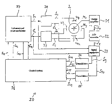
Figure 1 shows evaluation/control electronics 30 which
have a charge amplifier 31, an analog/digital converter
32, signal separation 33, a first demodulator 34, a
second demodulator 35, a control system 36, a two-
dimensional pulse modulator 37, a first and a second
force impulse conversion unit 38, 39 and a first to
fourth force transmitter electrode 401 to 404.
The entity formed by the components identified by the
reference numbers 31 to 40 forms two control loops: one
control loop for setting the amplitudes/frequencies of
the stimulation oscillation, and a further control loop
for setting the amplitudes/frequencies of the read
oscillation.
As Figure 1 shows, the circuit according to the
invention has only one analog/digital converter 32 and
no digital/analog converters. The digital/analog
converters are in this case replaced by the two-
dimensional pulse modulator 37 and the two force
impulse conversion units 38, 39.
The method of operation of the evaluation/control
electronics according to the invention will be
explained in more detail in the following text.
In order to set the amplitudes/frequencies of the
stimulation oscillation/read oscillation of the
resonator 2, the two-dimensional pulse modulator 37
produces a first and a second ternary-quantized output
signal S1, S2, with the first ternary-quantized output
signal S1 being converted in the first force impulse
conversion unit 38 to force impulse signals (voltage
CA 02524046 2005-10-27
- 19 -
signals) S3 and S4. In a corresponding manner, the
second ternary-quantized output signal S2 is converted
by the second force impulse conversion unit 39 to force
impulse signals (voltage signals) S5, S6. The ternary-
quantized output signals S1, S2 can preferably each
assume the values 1, 0 and -1.
If, for example, the signal S1 has the value +1, then
the first force impulse conversion unit uses the signal
S. to produce two force input signals S3 and S4, which
cause a force impulse. These force impulse signals S3
and S4 produce electromagnetic fields between the second
and the fourth of the force transmitter electrodes 402,
404 and between the force transmitter electrodes 402,
404 and the resonator 2, and these electromagnetic
fields result in force impulses. If the value of the
signal S1 is -1, then the force impulse signals S3 and
S4 are produced such that the lines of force of the
resultant electromagnetic fields run in the opposite
direction to the lines of force in the situation
S1 = 1. If the value of the signal S,_ is zero, there is
no electrical field between the second and fourth force
transmitter electrodes 402, 404 or between the force
transmitter electrodes 402, 404 and the resonator 2.
Thus, by way of example, the following potentials (0 or
Uo) are applied to the second and fourth force
transmitter electrodes 402, 404 in accordance with the
following table:
S1 404 402
-1 0 Uo
0 0 0
1 Uo 0
Corresponding considerations also apply to the second
ternary-quantized output signal S2, which is converted
by the second force impulse conversion unit 39 to a
fifth and a sixth force impulse signal S5, S6, which are
CA 02524046 2005-10-27
- 20 -
applied to the first and the third force transmitter
electrodes 401, 403. By way of example, the stimulation
oscillation parameters are set/controlled via the force
transmitter electrodes 402, 404, and the read
oscillation parameters are set/controlled via the force
transmitter electrodes 401, 403.
In addition to the stimulation of the resonator 2, the
application of electrical fields to the force
transmitter electrodes 401, 404 also results in
electrical charge flowing to a moving center electrode.
This charge is measured via the charge amplifier 31, a
corresponding analog output signal S7 is converted by
the analog/digital converter 32 to a corresponding
digital signal S8, from which the signal separation 33
produces a first digital read signal S9 and a second
digital read signal Slo. Since the charge which has
flowed to the center electrode is dependent on the
capacitances of those force transmitter electrodes 401,
404 to which an electrical field is applied at that
time, the amount of charge which has flowed is a
measure of the amplitudes/frequencies/other parameters
of the stimulation oscillation/read oscillation of the
resonator 2. The instantaneous movement/change in the
movement of the resonator 2 can thus be reconstructed
by the signal separation 33 as a function of the
instantaneous and/or older output signal values of the
ternary-quantized output signals Si, S2.
The two-dimensional pulse modulator 37 is
advantageously designed such that the ternary-quantized
output signals S. and S2 never change at the same time
since, in general, the charge which is flowing to the
center electrode is measured in sum form, that is to
say that charge movements which result from a
superimposition of two electrical fields can be
measured only as one entity, that is to say it is not
possible to associate parts of the charge movement with
individual electrical fields. The additional condition
CA 02524046 2005-10-27
- 21 -
between the ternary-quantized output signals S1 and S2
then makes it possible to obtain an unambiguous
association between the charge that has flowed and a
specific electrical field, so that it is possible to
distinguish precisely between the stimulation
oscillation and the read oscillation. A further
possible condition in this context is to state that
only one of the two signals S1 and S2 may assume values
other than zero at one specific time.
The first digital read signal S9 is demodulated by the
first demodulator 34 into a real part S11 and an
imaginary part S12. Analogously to this, the second
digital read signal Slo is demodulated by the second
demodulator 35 into a real part S13 and an imaginary
part S14. By way of example, the first digital read
signal S9 contains information about the stimulation
oscillation, and the second digital read signal Slo
contains information about the stimulation oscillation.
The real and imaginary parts S11 to S14 of the first and
second digital read signals S9, Slo are applied to the
control system 36, which produces stimulation/compensa-
tion signals S15 to S18 as a function of these signals.
By way of example, the signal S15 represents the real
part of the digital stimulation/compensation signal for
the stimulation oscillation, and the signal S16
represents its imaginary part, while, in contrast, the
signal S17 represents the real part of a digital
stimulation/compensation signal for the read
oscillation, and the signal S18 represents its imaginary
part.
The digital stimulation/compensation signals S15 to S18
are supplied to the two-dimensional pulse modulator 37,
which uses them to produce the ternary-quantized output
signals S1, S2.
Figure 3 shows a block diagram of the pulse modulator
according to the invention, in complex form. The
CA 02524046 2005-10-27
- 22 -
complex input signal x(t) has a real part and an
imaginary part, which are both represented as digital
values. The complex feedback signal 52 is subtracted
from the complex input signal x(t) in the addition node
51, with the difference between these two complex
signals representing the control error. Furthermore,
the (likewise complex) content of the delay element 53
is added to this difference in the addition node 51.
The content of the delay element 53 is passed via the
signal line 54 to the addition node 51. The delay
element 53 together with the signal line 54 forms a
complex integrator stage, which integrates the complex
control error, that is to say the difference between
the input signal and the feedback signal. The
integrated signal 55 is correspondingly amplified by
the factor "a" in the amplifier stage 56, and the
amplified signal 57 is passed to the first
multiplication stage 58, where the amplified signal 57
is multiplied by the complex mixing signal e-j'ot in
order in this way to obtain the signal 59, up-mixed to
the frequency c)o. The block 60 determines the real part
of the complex up-mixed signal 59, and the real part
61, obtained in this way, of the up-mixed signal is
made available to the quantizer 62.
In the embodiment shown in Figure 3, the quantizer 62
is in the form of a ternary quantizer, which converts
the respective input signal to the three possible
values -1, 0, +1 of a pulsed signal with the aid of
comparators. The quantized pulsed signal y(t) produced
in this way can be tapped off at the output of the
quantizer 62. The real pulsed signal y(t) is multiplied
in the second multiplication stage 63 by the complex-
conjugate mixing signal e-j"'-t in order to produce the
complex feedback signal 52. The complex feedback signal
52, which is obtained in this way by multiplication of
a real number and a complex number, is passed to the
addition node 51 at the input to the circuit.
CA 02524046 2005-10-27
- 23 -
The sequence of functional units illustrated in
Figure 3 can be implemented by means of a digital
signal processor (DSP) or else by means of hardware
that is specifically provided for this purpose. The
digital signal processing must in this case be carried
out at a sampling frequency mA, which is considerably
higher than the frequency wo of the complex mixing
signal. For example, 2 to 1000 times the mixing
frequency wo may be used as the sampling rate wA.
Figure 4 once again shows the pulse modulator
illustrated in Figure 3, with the in-phase signal path
and the quadrature signal path in this case being shown
separately. The upper half of Figure 4 shows the
in-phase signal path 64, which processes the real part
R of the input signal x(t) . The lower half of Figure 4
shows the quadrature signal path 65 for processing of
the imaginary part I of the input signal. The real part
of the control error is determined in the addition node
66 in the in-phase signal path as the difference
between the real part R of the input signal and the
real part 67 of the feedback signal. The integrator
value, which has been stored until then in the delay
element 68, is added to this control error, and is
passed via the signal line 69 to the addition node 66.
Together with the signal line 69, the delay element 68
forms an integrator with the transfer function
x(z) = 1_1 . Addition of the real part of the control
1 - z
error to the previous integrator value results in a new
integrator value, which is once again stored in the
delay element 68. The integrated signal 70 in the in-
phase signal path is scaled by the factor "a" by the
amplifier 71, and is passed as an amplified signal 72
to the first multiplier 73. The first multiplier 73
multiplies the real, amplified signal 72 by the real
signal cos((oot), that is to say by the real part of
ej c'ot. The first multiplier 73 determines the product
R=cos((oot), which is supplied as the signal 74 to the
CA 02524046 2005-10-27
- 24 -
adder 75.
The quadrature signal path 65 of the pulse modulator
has an addition node 76, in which the difference
between the imaginary part I of the input signal and
the imaginary part 77 of the feedback signal is
calculated. This difference, which corresponds to the
imaginary part of the control error, is added to the
previous content of the delay element 78, which is
passed to the addition node 76 via the signal line 79.
The new value, which is obtained as the sum of the
previous value and of the imaginary part of the control
error, is written to the delay element 78. Together
with the signal line 79, the delay element 78 forms an
integrator with the transfer function H(z)= 1. The
1 - z 1
integrated signal 80 from the quadrature signal path is
produced at the output of this integrator, and is
scaled by the factor "a" by the amplifier 81. The
amplified signal 82 obtained in this way in the
quadrature signal path is then multiplied by the signal
sin((oot) in the second multiplier 83. The product
I=sin(cwot) obtained in this way is supplied as the
signal 84 to the adder 75. The adder 75 adds the
signals R=cos(wot) and R=sin((oot) and produces the
signal R=cos(wot)+I=sin(wot) as the signal 85 at its
output. However, this signal 85 corresponds precisely
to the real part of the up-mixed signal, because the
complex multiplication of x(t) and e-j'ot gives:
x(t) = e-jw t =
= (R+j = I) = (cos (t)ot) -j = sin (wot) ) _
= [R = cos ((oot) +I = sin (wot) ] +j = [I = cos ((oot) -R = sin ((oot) ]
and the real part of this signal is
R=cos((oot)+I=sin(coot). The signal 85 thus represents
the real part of the complex up-mixed signal, and to
this extent corresponds to the signal 61 illustrated in
Figure 3.
CA 02524046 2005-10-27
- 25 -
The digital real signal 85 is passed to the quantizer
86, which converts this input signal to the quantized
pulsed signal y(t). The three-stage (ternary) quantizer
shown in the example in Figure 3 and Figure 4 quantizes
the input signal on the basis y(t)E{-1; 0; +1). For
this purpose, the quantizer 86 has comparators, which
compare the signal level of the signal 85 continuously
with predetermined threshold values. Depending on the
result of these comparisons, the output signal y(t) is
in each case assigned one of the values -1; 0; +1 as
the current signal value. Instead of the three-stage
(ternary) quantization, any other desired quantizations
may be used depending on the use purpose, for example
two-stage (binary) or multiple-stage quantizations.
The real part 67 and the imaginary part 77 of the
complex feedback signal are derived from the quantized
pulsed signal y(t). For this purpose, the pulsed signal
y(t) is multiplied by the complex-conjugate mixing
signal e+i'Ot :
y(t) =e''ot=y(t) =cos((oot)+j=y(t) =sin((oot)
The real part y(t)=cos((oot) of the complex feedback
signal is produced by the third multiplier 87, which
multiplies the pulsed signal y(t) by cos((oot). The real
part 67 of the feedback signal is thus produced at the
output of the third multiplier 87, and is fed back to
the addition node 66. In order to produce the imaginary
part y(t) = sin ((oot) of the complex feedback signal, the
pulsed signal y(t) is multiplied by sin(t)ot) in the
fourth multiplier 88. The imaginary part 77 of the
feedback signal is produced at the output of the fourth
multiplier 88, and is fed back to the addition node 76.
In the exemplary embodiments shown in Figures 3 and 4,
integrators are provided on the input side, which
integrate the control error between the input signal
CA 02524046 2005-10-27
- 26 -
and the feedback signal, and thus produce an integrated
signal. The transfer function H(z) of an integrator can
be written as H(z) = 11 . Other signal conversion
1 - z
stages with other transfer functions H(z) may also be
used on the input side, instead of the integrators. For
example, higher-order transfer functions H(z) could be
used in which case, however:
lim H(z) = ao
z-->l.
The transfer function H(z) should thus tend to infinity
for the situation in which the frequency w tends to the
value zero (z-->1). The additional free parameters of
H(z) may be used to optimize specific characteristics
of the modulator (for example the signal-to-noise
ratio) or of the overall system.
Figure 5 shows the waveform of the pulsed signal y(t)
which can be tapped off at the output of the quantizer
for the situation of ternary quantization with
y( t) E{-1; 0; +1 }, which was determined with the aid of
a computer simulation. In this case, the real part R of
the complex input signal was set to 0.3, while the
imaginary part I of the input signal was set to be
equal to zero. The input signal x(t) is thus constant,
and does not vary as a function of time. The sampling
frequency wA is five times as great as the mixing
frequency (oo/wA = 0.2. The clock pulses at the sampling
frequency aOA are shown on the abscissa, and are
numbered successively from 5000 to 5100. During each
clock cycle, the pulsed signal y(t) assumes one of the
three possible values -1; 0; +1. The respective value
of y(t) during one specific clock cycle at the sampling
frequency is plotted in the direction of the ordinate.
If a spectral analysis (FFT) is carried out on the
pulsed signal illustrated in Figure 5, this results in
CA 02524046 2005-10-27
- 27 -
the spectrum shown in Figure 6. The frequency of the
respective spectral components is shown in arbitrary
FFT units on the abscissa, while the signal intensity
is plotted in dB in the direction of the ordinate. A
peak can be seen in the spectral distribution at the
frequency wo. It can also be seen that the noise level
in the vicinity of the frequency wo is considerably
less than in the remaining part of the spectrum. In a
conventional sigma-delta modulator, the noise level
would in contrast be reduced considerably at low
frequencies, that is to say in the vicinity of the
frequency uoo. In the case of the pulse modulator
according to the invention, the integrated and
amplified signal is up-mixed to the mixing frequency wo
by means of a complex multiplication. In consequence,
the spectral range in which the noise is reduced is
also shifted toward the mixing frequency wo, thus
resulting in the noise characteristic illustrated in
Figure 6.
The pulse modulator according to the invention can be
used for digital synthesis of a pulsed signal, in which
case the main spectral component of the pulsed signal
can be predetermined by the mixing frequency wo. The
phase angle of the pulsed signal that is produced can
be set exactly by the ratio of the real part to the
imaginary part of the input signal, and this results in
a pulsed signal whose phase is stable. When using the
pulse modulator according to the invention for
frequency synthesis, the pulsed signal y(t) should be
filtered by means of an electrical bandpass filter,
whose pass band is centered around the frequency O.
This bandpass filter which, for example, may be in the
form of a crystal or ceramic filter, makes it possible
to suppress spectral ranges further away from cwo, in
which the noise level is undesirably high. A bandpass
filter such as this makes it possible to significantly
improve the signal-to-noise ratio.
CA 02524046 2005-10-27
- 28 -
The pulse modulator according to the invention is
suitable, inter alia, for stimulation of
electromechanical oscillators to carry out harmonic
oscillations. In particular, the electrostatic forces
which are required for oscillation stimulation can be
produced by means of a ternary-quantized pulsed signal
which is applied to the stimulation electrodes of a
micromechanical resonator. The frequency coo of the
pulsed signal y(t) is in this case preferably chosen to
be equal to the resonant frequency of the
micromechanical oscillator. If the pulsed signal as
illustrated in Figure 5 and Figure 6 is used for
harmonic stimulation of a high Q-factor oscillator (for
example with a Q-factor of 104), whose resonant
frequency corresponds to the stimulation frequency wo,
then the majority of the quantization noise is filtered
out by the oscillator itself. In particular, the
quantization noise in spectral ranges further away from
the resonant frequency wo is suppressed by the
oscillator itself. The filtered spectrum obtained in
this way is shown in Figure 7.
Specific ratios of the frequencies (0o/c)A exist for
which the noise-like quantization product in y(t) is
converted to a series of more or less periodic
functions. As one example of this, Figure 8 shows a
frequency spectrum which was obtained for the ratio
(00/0)A = 0.25. A range of spectral lines 89, 90, 91,
etc. can be seen in addition to the peak at the
frequency (oo. The reason for the creation of these
spectral lines is that the quantizer is a highly
non-linear element in the control loop, because this
stimulates relaxation oscillations in the control loop
with certain frequency ratios. This control loop
response is known from conventional delta-sigma
converters.
In order to prevent the creation of relaxation
oscillations, the central linearity of the quantizer
CA 02524046 2005-10-27
- 29 -
can be improved by adding a noise signal to the input
signal to the quantizer. A spectrally uniformly
distributed noise signal is preferably used for this
purpose. Figure 9 shows the block diagram of a
correspondingly modified pulse modulator. In comparison
to the block diagram shown in Figure 4, the pulse
modulator shown in Figure 9 additionally has a noise
generator 92, which produces a noise signal 93. In
addition, the integrators which are shown in Figure 4
are illustrated in a generalized form as signal
conversion stages 94, 95 with the transfer function
H(z). Otherwise, the assemblies shown in Figure 9
correspond to the elements of the block diagram in
Figure 4. The noise signal 93 is supplied to the adder
75, where it is added to the signals 74 and 84. The
signal 85 at the input of the quantizer 86 therefore
has a noise signal superimposed on it, and, in the end,
this leads to statistical rounding in the quantization
process. Figure 10 shows the frequency spectrum of a
pulsed signal y(t) which was produced with the aid of a
pulse modulator modified as shown in Figure 9. Although
the frequency ratio wo/(OA is once again equal to 0.25,
no relaxation oscillations are formed.
The pulse modulator according to the invention can be
used in particular for electrostatic stimulation of
micromechanical oscillators. For this purpose, by way
of example, a ternary-quantized pulsed signal of the
type shown in Figure 5 can be connected to the
stimulation electrodes of a micromechanical resonator.
The pulsed signal shown in Figure 5 represents a
sinusoidal signal at the frequency c)o. A pulsed signal
such as this can thus be used to stimulate a
micromechanical resonator to carry out harmonic
oscillations at the frequency wo, to be precise in
particular when the frequency wo of the pulsed signal
corresponds at least approximately to the resonant
frequency of the oscillator.
CA 02524046 2005-10-27
- 30 -
Resonators which can oscillate in two mutually
perpendicular directions yl and y2 are used in rotation
rate sensors and Coriolis gyros. The two-dimensional
pulse modulator shown in Figure 11 may preferably be
used for electrostatic stimulation of a resonator with
two degrees of freedom. The two-dimensional pulse
modulator has a first pulse modulator 96, which
produces the pulsed signal yl(t) from the complex input
signal R1, I1, and this pulsed signal is used to
stimulate the resonator in the yl direction. The pulsed
signal y2(t) is produced from the complex input signal
R2, 12 by the second pulse modulator 97, and this pulsed
signal is used to stimulate the oscillator to oscillate
in the y2 direction. Both the first pulse modulator 96
and the second pulse modulator 97 are in the form of a
pulse modulator with statistical rounding as shown in
Figure 9. A description of the design and method of
operation of the first and of the second pulse
modulator 96, 97 can therefore be found in the
description of the figures relating to Figures 4 and 9.
However, the two-dimensional pulse modulator shown in
Figure 11 has one 2D quantizer 98 which is shared by
the two channels and converts the signal 99 of the
first pulse modulator 96 to the quantized pulsed signal
yl(t), and transforms the signal 100 of the second
pulse modulator 97 to the quantized pulsed signal
y2 (t) . The use of a 2D quantizer 98 which is shared by
the two channels makes it possible during the
quantization of the signals 99, 100 to take into
account additional conditions which are advantageous
for operation of the micromechanical sensor. One such
additional condition, by way of example, is that in
each case only one of the channels may produce pulses
other than zero. Another feasible additional condition
is that only one of the output signals yl (t) , y2 (t) may
change in each case at any given time. Additional
conditions such as these may be worthwhile when the
displacement currents which are applied to the
electrodes of a double resonator are measured in sum
CA 02524046 2005-10-27
- 31 -
form, in order to make it possible to deduce the
deflection of the oscillator. The additional conditions
make it possible to unambiguously associate a
displacement current with one specific electrode. This
makes it possible to carry out signal separation
between the signals caused by the yl deflection and the
Y2 deflection of the oscillator.
All of the embodiments of the pulse modulator according
to the invention that have been described above can be
used to carry out the method according to the invention.
If required, they may be combined with one another. The
pulse modulator (two-dimensional) described in Figure
11 can be adopted "directly", and it is also possible
to use combinations of two one-dimensional pulse
modulators. It is also possible to dispense with the
addition of the additional noise signal.