Note: Descriptions are shown in the official language in which they were submitted.
CA 02525530 2005-11-10
WO 2004/102144 PCT/US2004/015274
HIGH TEMPERATURE PRESSURE SENSITIVE DEVICES AND METHODS
THEREOF
RELATED APPLICATIONS
This application claims the benefit of U.S. Provisional Patent Application
Ser. No.
601470,614, filed May 14, 2003, entitled "High Temperature Pressure Sensitive
Devices and
Methods Thereof," by Lima, et al., incorporated herein by reference.
FIELD OF INVENTION
to The present invention relates to pressure sensitive materials, devices
incorporating
such pressure sensitive materials, and methods of fabricating and using such
pressure
sensitive materials and devices under high temperature conditions.
BACKGROUND OF THE INVENTION
~s Pressure sensitive materials, such as those derived from solidified
pressure sensitive
inky-respond in some way to an applied force. For some solidified pressure
sensitive inks,
their electrical resistivity or conductivity varies as a function of the
applied pressure.
Pressure sensitive ink has been used for various tactile or pressure sensitive
devices such as
pressure transducers, sensors, and strain gauges. For example, Maness, et al.,
in U.S. Patent
2o Nos. 4,734,034 and 4,856,993, describe a contact sensor for measuring
dental occlusion.
Also, McDowell, in U.S. Patent No. 5,541,570, describes a force sensing
solidified ink as
well and methods of making the ink as well as an improved force sensor. And,
Krivopal, in
U.S. Patent No. 5,989,700, describes a pressure sensitive ink and methods of
its use.
2s BRIEF SUMMARY OF THE INVENTION
The present invention is directed to pressure sensitive materials and pressure
sensitive
inks, as well as to pressure sensitive devices incorporating or utilizing such
pressure sensitive
materials. More particularly, the present invention is directed to temperature
stable pressure
sensitive materials and pressure sensitive inks forming such pressure
sensitive materials, and
so to temperature stable pressure sensitive devices having electrical
properties that can vary
predictably at high temperature. The subject matter of the present invention
involves, in
some cases, interrelated products, alternative solutions to a particular
problem, andlor a
plurality of different uses of one or more systems and/or articles.
CA 02525530 2005-11-10
WO 2004/102144 PCT/US2004/015274
-2-
In accordance with one or more embodiments, the present invention provides a
pressure sensitive device comprising a nonconductive supporting substrate
comprising a
polyimide, a conductive lead supported by the substrate and comprising silver
particles
dispersed in a polyhydroxy ether crosslinked with melamine formaldehyde, a
pressure
sensitive material in contact with the conductive lead and supported by the
substrate
comprising conductive carbon nanoparticles dispersed in an polymeric matrix
selected from
the group consisting of a silicone rubber, a polyamide-imide polymer, a
polyester-imide
polymer, a poly(vinylidene fluoride-hexafluoropropylene), a poly(acrylonitrile-
butadiene-
styrene), a polyethylene-2,6-naphthalene Bicarbonate), a poly(bisphenol-A
carbonate), a
1o polyhydroxy ether resin crosslinked with melamine formaldehyde, a product
of a
polycondensation reaction of a dianhydride and a diamine, or combinations
thereof, and an
adhesive material supported by the substrate and comprising a synthetic rubber
material and a
silane coupling agent.
In accordance with one or more embodiments, the present invention provides a
1s pressure sensitive device. The pressure sensitive device comprises a
nonconducting
supporting substrate, and a pressure sensitive material supported by the
substrate and
comprising conductive carbon nanoparticles dispersed in a polymeric matrix
selected from
the group consisting of a silicone rubber, a polyamide-imide polymer, a
polyester-imide
polymer, a poly(vinylidene fluoride-hexafluoropropylene), a poly(acrylonitrile-
butadiene-
2o styrene), a polyethylene-2,6-naphthalene Bicarbonate), a poly(bisphenol-A
carbonate), a
polyhydroxy ether resin crosslinked with melamine formaldehyde, a product of a
polycondensation reaction of a dianhydride and a diamine, or combinations
thereof.
In accordance with one or more embodiments, the present invention provides a
pressure sensitive device having a variation in electrical conductivity in
response to an
2s applied force. The pressure sensitive device comprises a substrate
comprising a polyimide,
and a means for varying the electrical conductivity in response to the applied
pressure, where
the means has a conductivity of about 0.01 p.S to about 1300 wS and a
sensitivity of about
0.01 ~,Sllb to about 300 ~,S/lb over a temperature range of about 80 °F
to about 220 °F. In
some cases, the means for varying the electrical conductivity can be supported
on the
so substrate.
In accordance with one or more embodiments, the present invention provides a
pressure sensitive material comprising carbon nanoparticles dispersed in a
polymeric matrix
CA 02525530 2005-11-10
WO 2004/102144 PCT/US2004/015274
-3-
such that said pressure sensitive ink has a conductivity of about 0.01 pS to
about 1300 ~.S and
a sensitivity of about 0.01 ~S/lb to about 300 ~S/lb over a temperature range
of about 80 °F
to about 220°F. In some cases, the temperature range may be of about -
50 °F to about 400 °F
or 420 °F.
In accordance with one or more embodiments, the present invention provides a
method of fabricating a pressure sensitive device. The method comprises steps
of providing a
supporting nonconductive substrate, depositing a first electrical conductor
and a second
electrical conductor on a portion of the substrate, and depositing a pressure
sensitive layer on
at least a portion of the substrate in electrical communication with the first
and second
1o electrical conductors. In some cases, the pressure sensitive layer
comprises carbon
nanoparticles dispersed in a polymeric material. In one embodiment, the
pressure sensitive
device may be non-planar.
In accordance with one or more embodiments, the present invention provides a
method of fabricating a pressure sensitive device. The method comprises steps
of providing a
~s supporting nonconductive substrate, depositing a first electrical lead and
a second electrical
lead on a portion of the substrate, and depositing a pressure sensitive
material on at least a
portion of the substrate in electrical communication with the first and second
electrical leads.
In some cases, the pressure sensitive material has properties such that an
electrical
conductance measured across the electrical leads varies in response to an
applied force such
2o that it has a conductivity of about 0.01 ~.S to about 1300 ~S and a
sensitivity of about 0.01
~S/lb to about 300 wS/lb over a temperature range of about 80 °F to
about 220 °F. In one
embodiment, the pressure sensitive device may be non-planar.
In accordance with one or more embodiments, the present invention provides a
method of determining force applied to a pressure sensitive device. The method
comprises
25 steps of applying a force on a pressure sensitive material comprising
carbon nanoparticles
dispersed in a polymeric matrix, and measuring a resultant conductivity across
the pressure
sensitive material. The pressure sensitive material, in one embodiment, has a
conductivity of
about 0.01 pS to about 1300 ~S and a sensitivity of about 0.01 ~S/lb to about
300 wS/lb over
a temperature range of about 80 °F to about 220 °F.
3o In accordance with one or more embodiments, the present invention provides
a
pressure sensitive device comprising a nonconducting supporting substrate, and
a pressure
sensitive material supported by the substrate and comprising conductive carbon
particles
CA 02525530 2005-11-10
WO 2004/102144 PCT/US2004/015274
-4-
dispersed in an polymeric matrix selected from the group consisting of
polyvinylidene
fluoride, a reaction product of a phenoxy and at least about 10 wt% melamine,
or
combinations thereof.
Other advantages and novel features of the present invention will become
apparent
from the following detailed description of various non-limiting embodiments of
the invention
when considered in conjunction with the accompanying figures. In cases where
the present
specification and a document incorporated by reference include conflicting
and/or
inconsistent disclosure, the present specification shall control.
to BRIEF DESCRIPTION OF THE SEVERAL VIEWS OF THE DRAWINGS
The accompanying drawings are not intended to be drawn to scale. In the
drawings,
typically each identical or nearly identical component that is illustrated in
various figures is
represented by a like numeral. For purposes of clarity, not every component
may be labeled
in every drawing. In the drawings:
is FIG. 1 is a cross-sectional diagram of a solidified pressure sensitive ink,
according to
one or more embodiments of the invention;
FIG. 2 is plan view of a solidified pressure sensitive device, according to
one or more
embodiments of the invention;
FIG. 3 is a cross-sectional view through section 3-3 of an assembled pressure
2o sensitive device shown in FIG. 2;
FIG. 4 is graph showing conductivity as function of applied pressure of a
polyimide
pressure sensitive material-based pressure sensitive device at various
temperatures, according
to one or more embodiments of the invention;
FIG. 5 is a graph showing sensitivity as a function of temperature of a
polyimide-
25 based pressure sensitive device, according to one or more embodiments of
the invention;
FIG. 6 is graph showing sensitivity as a function of temperature of a
polyimide-based
pressure sensitive device, according to one or more embodiments of the
invention, as well as
the sensitivity of a standard pressure sensitive device known in the art;
FIG. 7 is a graph showing sensitivity as a function of temperature of various
high
3o temperature capable pressure sensitive device, according to one or more
embodiments of the
invention;
CA 02525530 2005-11-10
WO 2004/102144 PCT/US2004/015274
-5-
FIG. 8 is a graph showing the conductivity through several loading cycles at
room
temperature of a polyimide pressure sensitive material-based pressure
sensitive device,
according to one or more embodiments of the invention; and
FIG. 9 is a graph showing sensitivity as a function of the percentage of
carbon
nanoparticles in the film matrix, according to one or more embodiments of the
invention.
DETAILED DESCRIPTION OF THE INVENTION
As used herein, the phrase "pressure sensitive material" refers to a solid
material,
typically a polymeric material, having at least one material property, other
than shape or,
1o density, typically electrical resistivity, or conductivity, that
predictably varies as a function of
the force applied to the material. The phrase "pressure sensitive ink," as
used herein, refers
to a fluent material that, upon solidification via, e.g., polymer curing
and/or polymerization
and/or solvent evaporation, forms a pressure sensitive material.
In accordance with one or more embodiments, the present invention provides a
15 pressure sensitive ink able to form a pressure sensitive material having a
selected pressure
sensitivity designed for use as the pressure sensitive component of a pressure
sensitive
device. The solidified pressure sensitive ink can comprise carbon
nanoparticles dispersed in
a polymerized polyimide matrix. The solidified pressure sensitive ink can have
a
conductivity of between about 0.01 microSiemens (~.S) to about 1300 ~5,
typically about 200
20 ~S to about 1 milliSiemen (mS), with a sensitivity of about 0.01 ~.S/lb to
about 300 pS/lb
(about 0.02 ~.S/kg to about 660 ~S/kg), and in some cases between about 250
~S/lb and about
300 ~S/lb (about 550 ~S/kg and about 660 ~S/kg), over a temperature range of
from about 80
°F to about 220 °F (about 27 °C to about 105 °C),
and in certain embodiments, over a
temperature range of from about -50 °F to about 350 °F, about
400 °F, or about 420 °F (about
2s -45 °C to about 176 °C, about 205 °C, about 216
°C) or greater. The polyimide matrix can
comprise a polycondensation reaction product of a dianhydride and a diamine in
one set of
embodiments.
One embodiment of an inventive pressure sensitive ink or pressure sensitive
material
or layer is shown in FIG. 1. Pressure sensitive material 10 can comprise an
elastomeric or
3o polymeric binder or matrix 11 incorporating, typically substantially
uniformly therethrough, a
plurality of particles 12 which may be conductive or semiconductive, such that
the pressure
sensitive material 10, when cured and/or dried, provides a response that can
be represented as
CA 02525530 2005-11-10
WO 2004/102144 PCT/US2004/015274
-6-
a change in electrical resistivity or conductivity upon the application and/or
relaxation of a
pressure or force P, designated by reference number 16, applied to material
10. That is, in
one or more embodiments, pressure sensitive material 10 and/or a composite
structure having
a plurality of layers 10 at least partially overlaying each other can provide
an increase in
s electrical conductive pathways upon the application of a force or pressure.
This may result in
an increase in electrical conductivity such that the conductivity (or the
change of
conductivity) can be measured, which may be an indication of the magnitude of
the force or
pressure applied. The polymeric/elastomeric matrix 11 may be comprised of one
or more of
the high temperature stable polymers, e.g., as described below. In some cases,
pressure
1o sensitive material 10 can further comprise a dielectric material 14 mixed
with and/or forming
at least a part of the elastomeric matrix 11. In certain instances, the
elastomeric matrix 11
can further incorporate fillers 18, e.g. reinforcing or non-reinforcing
fillers, that can be
tailored to provide variations in the mechanical and/or chemical properties of
pressure
sensitive layer 10, as would be understood by those skilled in the art.
15 In accordance with one or more embodiments, the present invention provides
a
pressure sensitive device. The pressure sensitive device can comprise a
supporting
nonconductive substrate; conductive leads) supported by the substrate,
comprising
electrically conductive metal dispersed in a polymeric matrix; and a pressure
sensitive
material supported by the substrate and electrically connected to the
conductive lead(s). The
2o pressure sensitive material can comprise solidified pressure sensitive ink
with carbon
particles dispersed in a polymeric matrix such as polyimide, i.e. cured
polyamic acid. In
some embodiments, the pressure sensitive material can comprise conductive
carbon
nanoparticles dispersed in an elastomeric matrix. The material, in some cases,
can comprise
any one or more of a product of a polycondensation reaction of a dianhydride
and a diamine;
25 a polyamide-imide polymer; polyester-imide polymer; a poly(vinylidene
fluoride-
hexafluoropropylene); a poly(acrylonitrile-butadiene-styrene); a polyethylene
2,6-
naphthalene dicarbonate); a poly(bisphenol-A carbonate); as well as
combinations of these
and/or other materials.
The pressure sensitive device may be constructed from materials and components
that
3o provide improved high temperature capability and/or stability, for example,
in certain
embodiments, at operating temperatures from about -50 °F (about -45
°C) to greater than
about 150 °F (about 65 °C), and for some embodiments as much as
about 350 °F, about 400
CA 02525530 2005-11-10
WO 2004/102144 PCT/US2004/015274
-7-
°F, or about 420 °F (about 176 °C, about 205 °C,
or about 216 °C), and sometimes more.
Typical devices have improved conductivities and sensitivities ranging from
about 0.01 ~ S to
about 1300 ~,5. In some embodiments, the pressure sensitive devices are
constructed of
materials and components that provide improved high temperature capabilities
with
sensitivities of about 0.01 ~,S/lb to about 300 ~S/lb (about 0.02 ~,S/kg to
about 660 pS/kg),
and in some cases between about 250 ~.S/lb and about 300 ~.S/lb (about 550
wS/kg and about
660 ~S/kg) over a temperature range from about 80 °F to about 220
°F (about 27 °C to about
105 °C), or even from about -50 °F to about 350 °F, about
400 °F, or about 420 °F (about -45
°C to about 176 °C, about 205 °C, or about 216 °C)
or greater in some cases. The pressure
l0 sensitive material may provide a variation in electrical
conductivity/resistivity corresponding
to an applied force or pressure. Certain embodiments also provide a pressure
sensitive device
that are constructed of materials and components that provide improved
hysterisis and drift
performance at certain high temperature conditions.
Typical pressure sensitive devices in which the pressure sensitive inks and/or
pressure
sensitive materials of this invention can be used include pressure
transducers, such as load
cells, button cells, strain gauges, pressure gauges, and other pressure
sensors. For example,
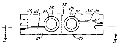
FIG. 2 shows an example pressure sensitive device 20 according to one
embodiment of the
present invention. The pressure sensitive device 20 incorporates pressure
sensitive layers 10
in a button cell assembly in this figure. The pressure sensitive device 20 has
a layer or
2o substrate 21 providing structural support for assembled pressure sensitive
device 20, shown
in a cross-sectional view in FIG. 3. As will be further described below,
substrate 21 may be
insulating and/or non-conductive and, in certain embodiments, may comprise a
polyimide
film. Substrate 21 is defined into a first segment 27 and a second segment 28
by a centerfold
line 23 in Fig. 2. Further, the pressure sensitive device 20 has electrically
conductive leads
2s 22 and 24 deposited on a surface of substrate 21; the first conductive lead
22 is deposited on
first segment 27 and the second conductive lead 24 is deposited on second
segment 28.
Substrate 21 and conductive leads 22 and 24 may be mechanically and/or
chemically stable at
over a temperature range, including temperatures of at least about -50
°F (about -45 °C) to
temperatures of at least about 150 °F (about 65 °C), as well as
temperatures up to and
3o including at least about 350 °F, about 400 °F, or about 420
°F (about 176 °C, about 205 °C, or
about 216 °C).
CA 02525530 2005-11-10
WO 2004/102144 PCT/US2004/015274
-g_
Conductive leads 22 and 24 can further comprise conductive portions 25 and 26,
respectively, which can be thin and highly conductive, and can be disc- or
circularly- or
square-shaped in some cases. The conductive leads 22 and 24 as well as round
conductive
portions 25 and 26, in certain embodiments, may have a resistivity in the
range of from about
s 10-6 to 10~ ohm-centimeters. Conductive leads 22 and 24 can be connected to
conventional
electrical testing or measurement apparatus for measuring resistivity or
conductivity, such as
those described in U.S. Patent No. 4,734,034.
The pressure sensitive device 20 may further comprise, deposited thereon, a
solidified
pressure sensitive ink or other pressure sensitive material comprising layers
10, for example,
on either side of center line 23 in the illustrated embodiment of Fig. 2. A
solidified pressure
sensitive ink or other pressure sensitive material may be deposited on
conductive portions 25
and 26, and symmetrically spaced so as to overlie each other as when pressure
sensitive
device 20 is folded along line 23, thereby creating a non-planar device. As
shown in the
embodiment of FIG. 3, the assembly of pressure sensitive device 20 includes a
folding of the
device along the line 23 to form a sandwich layer structure.
Pressure or force on the pressure sensitive device 20, as designated by arrow
30 in
Fig. 3, induces a variation in the contact electrical conductance between the
pressure sensitive
layers and/or within one or both of layers 10, which can be measured across
conductive leads
22 and 24 (not visible). The magnitude of the contact conductance between the
pressure
2o sensitive layers 10 may vary with the magnitude of the applied force 30.
This change in
resistivity/conductivity with increasing or decreasing pressure can be
measured by standard
electronics, as known in the art. Pressure sensitive layers 10 can be
deposited with a plurality
of layers in a variety of thicknesses, for example, ranging from about 0.2 mil
to about 2 mil
(about 5 micrometers to about 50 micrometers).
In one or more embodiments according to the present invention, the supporting
substrate can comprise a polyimide resin. Examples of commercially available
polyimide
resins which can be used as the supporting substrate include, but are not
limited to,
KAPTON~ polyimide film available from E. I. DuPont de Nemours and Company,
Wilmington, Delaware, or APICALTM polyimide film, available from Kaneka High-
Tech
3o Materials, Inc., Pasadena, Texas. Other suitable commercially available
materials for the
substrate include liquid crystalline polymer films) such as those available
from Foster-
Miller, Inc., Waltham, Massachusetts, or polyethylene naphthalene (PEN) such
as
CA 02525530 2005-11-10
WO 2004/102144 PCT/US2004/015274
-9-
KALADEX~ PEN film available from E. I. DuPont de Nemours and Company,
Wilmington,
Delaware. The substrate may provide support for the components of the pressure
sensitive
device when assembled as described below, and in some cases, be sufficiently
flexible when
a force is applied thereon such that it minimally, if at all, affects the
applied force. That is, it
provides negligible resistance in response to the applied force. The device
can be constructed
from materials that enable it to be mechanically and/or chemically stable in
service,
including service over a temperature range from about 80 °F to about
220 °F (about 27 °C to
about 105 °C), and in certain embodiments, over a temperature range of
from about -50 °F to
about 350 °F, about 400 °F, or about 420 °F (about -45
°C to about 176 °C, about 205 °C,
~o about 216 °C) or greater.
In one or more embodiments according to the present invention, the conductive
lead
or layerof an inventive pressure sensitive device can comprise a solidified
electrically
conductive ink. The conductive layer or solidified conductive ink can be
configured in the
device such that it provides electrical communication to external
instrumentation to and from
~ 5 the pressure sensitive component of the device, which may be formed from a
pressure
sensitive material or solidified pressure sensitive ink of the invention. Like
the other
components, the material of the conductive layer may preferably be
mechanically and/or
' chemically stable in service, including in certain embodiments service at
temperatures of
between about -50 °F (about -45 °C) to greater than about 150
°F (about 65 °C), and in
2o certain embodiments up to about 220 °F (about 105 °C) and, in
yet other embodiments, up to
about 350 °F, about 400 °F, or about 420 °F (about 176
°C, about 205 °C, or about 216 °C) or
more. In some embodiments, the conductive lead or layer can comprise silver
particles
dispersed in a crosslinked polymeric matrix. In certain embodiments, the
crosslinked
polymeric matrix can comprise a reaction product of a polyhydroxy compound and
a
2s crosslinker compound. The polyhydroxy compound can be selected from one or
more of a
phenoxy compound; an epoxy compound; an acrylic polyol compound; hydroxyl-
functional
polyester compound; a hydroxyl-functional polyether compound; a polyvinyl
alcohol
compound; and/or a polyvinyl butyral compound, as well as combinations of
these and/or
other polyhydroxy compounds. Examples of suitable phenoxy compounds include,
but are
3o not limited to, 4,4'-(methylethylidene)bispolymer with chloromethyl oxirane
such as those
commercially available as PAPHEN~, PKHC~, PKHH~, PKHJ~, PKHP~, and PKFE~
phenoxy resins available from Phenoxy Specialties, Inc., Rock Hill, South
Carolina. Other
CA 02525530 2005-11-10
WO 2004/102144 PCT/US2004/015274
-10-
non-limiting examples of suitable conductive materials include those described
by Krivopal
in U.S. Patent No. 5,989,700, which is incorporated herein by reference in its
entirety.
The crosslinker can comprise any one or more of melamine formaldehyde, phenol
formaldehyde, urea formaldehyde, anhydrides, amines (e.g., primary or
secondary amines),
s dianhydrides, polyanhydrides, diisocyanates, polyisocyanates, polyurethane
prepolymers, and
silanes, as well as combinations of these and/or other suitable crosslinker
compositions. For
instance, suitable non-limiting examples of commercially available melamine
formaldehyde
material include ISOMINTM, MELAICARTM, MELBRITETM, MELMEXTM, MELOPASTM,
RESARTTM, RESIMINE~, and ULTRAPAS~. In some embodiments, the crosslinker is a
1o phenol formaldehyde or a phenolic resin, such as BAKELITETM resin available
from Bakelite
AG, Iserlohn, Germany, SANTOLINI~TM resin available from Solutia, Inc., St.
Louis,
Missouri, or resins from the Georgia Pacific GPRI 7000 resin family, available
from Gerogia
Pacific, Atlanta, Georgia.
For example, in some embodiments, the conductive ink can comprise about 10 wt%
to
1s about 30 wt% solvent (described below), about 5 wt% to about 20 wt%
polymeric matrix,
and at least about 55 wt% silver particles. The conductive ink can optionally
comprise up to
about 2 wt% of an additive such as adhesion promoters, surface tension
modifiers, antifoam
agents, viscosity modifiers, coloring pigments, or the like, as well as
combinations of these
and/or other suitable materials. Those of ordinary skill in the art can
readily select such
20 additives to achieve any desired properties. Specific non-limiting examples
of commercially
available conductive preformed silver ink useable as the conductive layer of
certain
embodiments of the invention include those that are commercially available,
e.g., DUPONT
5028, DUPONT 5025, or DUPONT 6492 conductive ink, each available from E. I.
DuPont
de Nemours and Company, Wilmington, Delaware, and ELECTRODRAG~ 478SS and
25 479SS silver based polymer thick film inks, available from Acheson Colloids
Company, Port
Huron, Michigan. of suitable materials that can be used in the conductive ink
utilized in the
devices of the present invention include organometallic inks that can form
films of high metal
content and, hence, can be very conductive. Non-limiting examples of
organometallic inks
include Parmod TKA-100 and Parmod VLT, each available from Parelec, Inc.,
Rocky Hill,
3o New Jersey.
In some cases, the conductive ink can comprise additives such as wetting
agents,
dispersing agents, de-foaming agents, leveling agents, and/or adhesion
promoters, and any
CA 02525530 2005-11-10
WO 2004/102144 PCT/US2004/015274
-11-
additives so added may be, for example, between about 0.05% and 0.5% of the
total binder
weight.
In one or more embodiments according to the present invention, the pressure
sensitive
material comprises a polymeric, optionally elastomeric, matrix, which can
comprise a product
of a polycondensation reaction of a dianhydride with a diamine. In some
embodiments, the
carbon nanoparticles can be dispersed in the elastomeric matrix at a loading
of about 2 wt%
to about 9 wt%. The elastomeric matrix may further comprise a filler, such as
a reinforcing
filler including, but not limited to, fumed silica dioxide.
In some embodiments, the pressure sensitive material comprises a
1o polymeric/elastomeric matrix comprising a polyimide resin. In some cases,
the polyimide
resin may be cured polyamic acid resin. Examples of commercially available
polyamic acid
resins that can be used in accordance with the present invention include, but
are not limited
to, the SKYBOND~ resin family, such as the SKYBOND~ 700 series MDA free resin,
the
SKYBOND~ 703 series BTDA/1VIDA based resin, and the SKYBOND~ 705 series film
formable resin, each available from Industrial Summit Technology, Parlin, New
Jersey.
Other suitable examples of commercially available polyamic acid resins include
MATRIMID~ 5218 and 5292 resins, each available from Vatico AG, Basel,
Switzerland; the
DUR1MIDETM 100 series, 7000 series, 7500 series, and 7800 series resins,
available from
Arch Chemicals, Inc., Norwalk, Connecticut; the VESPEL~ resin family available
from
2o DuPont Engineering Polymers, Newark, Delaware; as well as HL-P200 resin, HL-
P500 resin,
and HL-P800 resin, each available from Hitachi Chemicals Co., Ltd., Tokyo,
Japan. Non-
limiting examples of commercially available polyimide resins include Probimide
348;
Probimide 412, and XU-287 from Ciba-Geigy, Basel, Switzerland; PI-2540, PI-
2545, PI-
2560, PI-5878, Pylarin PI-2611, and Piralux from DuPont; and PI QL 100, PI XL
110 from
Hitachi.
For embodiments utilizing a pressure sensitive material comprising a reaction
product
of a dianhydride with a diamine, the dianhydride can potentially comprise any
one or more of
pyromellitic dianhydride or 1,2,4,5-tetracarboxylic benzene dianhydride
(PDMA), 3,4,3',4'-
benzophenone tetracarboxylic benzene dianhydride (BTDA), 3,4,3',4'-biphenyl
3o tetracarboxylic dianhydride (BPDA), terphenyl tetracarboxylic dianhydride
(TPDA),
3,3',4,4'-oxydiphthalic dianhydride (OPDA), 2,2'-bis[4-(3,4-
dicarboxyphenoxy)phenyl]propane dianhydride (BPADA), 3,3',4,4'-diphenylsulfone
CA 02525530 2005-11-10
WO 2004/102144 PCT/US2004/015274
-12-
tetracarboxylic dianhydride (DSDA), bis(3,4-dicarboxyphenyl)dimethylsilane
dianhydride
(SiDA), as well as combinations of these and/or other dianhydrides. The
diamine can
potentially comprise any one or more of 4,4'-oxydiamine, 4,4'-diamino diphenyl
or 4-amino
phenyl ether, 4,4'-methylenedianiline (ODA), 4,4'-diamino diphenyl methane
(MDA), meta-
l phenyl diamine (MPD), 1,3-phenylene diamine (1,3-PDA), 1,4-phenylene diamine
(1,4-
PDA), isophorone diamine (IPDA), (1,1'-biphenyl)-4,4'-diamine (DAF),
1,3-bis(3-aminophenoxy)benzene (APB-133), 1,3-bis(4-aminophenoxy)benzene (APB-
134),
durene diamine or 2,3,5,6-tetramethylphenylenediamine (DAD), as well as
combinations of
these and/or other diamines. Some suitable combinations of dianhydride with
diamine
~o include, but are not limited to, PDMA with ODA, BPDA with ODA, BPDA with
MDA,
BPTA with NmA, ODPA with ODA, BTDA with ODA, BTDA with MDA, P1V~A with
PDA, BTDA with PDA, and PMDA with MPD.
The fluent pressure sensitive ink suitable for use in the pressure sensitive
device
according to one embodiment of the present invention can comprise up to about
85 wt% of a
15 suitable solvent, from about 15 wt% to about 95 wt% polymeric material, and
about 1 wt% to
about 30 wt% carbon particles (dry weight). The relative amount of the
starting materials
comprising the polymeric matrix can be varied to achieve desired physical
properties. For
example, the polyimide resin can comprise a product of a reaction of a diamine
and a
dianhydride. In some cases, substantially equimolar amounts of diamine and
dianhydride
2o may be used; in other cases, the relative amounts of each can be adjusted
as necessary to
target certain desired physical properties. Some polyimide precursors may be
commercially
available in the form of polyamic acids. To slightly modify the pressure
sensitive ink for
improved processing and other properties, in some cases, the pressure
sensitive ink can
further have up to about 2 wt% of one or more additives such as adhesion
promoters, surface
2s tension modifies, antifoaming agents, viscosity modifies, pigments, or the
like, as well as
combinations of these and/or other suitable additives. Those of ordinary skill
in the art can
readily select the amount and type of additive using no more than routine
experimentation to
achieve a desired set of properties.
In accordance with yet other embodiments, the pressure sensitive device may
further
so comprise a dielectric material that is able to electrically isolate the
conductive lead or layer
from other conductive leads or layers. For example, a dielectric material can
be deposited
adjacent, on, or both adjacent and on one or more conductive leads to prevent
electrical
CA 02525530 2005-11-10
WO 2004/102144 PCT/US2004/015274
-13-
communication with another conductive lead or layer. The dielectric material
can comprise,
for example, a polyhydroxy ether resin and/or a polyhydroxy ether resin
crosslinked with
melamine formaldehyde. Examples of polyhydroxy ether resins and crosslinking
compounds
suitable for use as the dielectric material include, but are not limited to,
those discussed above
as useful forming the pressure sensitive material. Other polymers and polymer
systems that
might be used for high temperature dielectrics include polyimide resulting
from the reaction
of a dianhydride and a diamine.
Specific non-limiting examples of commercially available products suitable for
use as
the dielectric material include, but are not limited to, the SKYBOND~
polyimide resin
1o family, such as the SKYBOND~ 700 series MDA free polyimide resin, the
SKYBOND~ 703
series BTDA/1VIDA based polyimide resin, and the SKYBOND~ 705 series film
formable
polyimide resin, each available from Industrial Summit Technology, Parlin, New
Jersey;
DUPONT 50186 and 5036 resins, available from E. I. DuPont de Nemours and
Company,
Wilmington, Delaware; ELECTRODRAG~ 451SS and 452SS resins available from
Acheson
Colloids Company, Port Huron, Michigan. In some cases, phenoxy resins
crosslinked with
one or more of melamine formaldehydes, phenolics, urea formaldehydes,
anhydrides,
diisocianates, and silanes may be potentially useful in high temperature
dielectric materials.
Other potentially useful polymers include acrylic polyols, polyesters with
hydroxyl
functionality, polyvinyl alcohols, polyvinyl butyral, crosslinked with any of
the following
2o material: melamine formaldehydes, pheonolics, urea formaldehydes,
anhydrides,
diisocianates and silanes. LTV curable dielectric pastes based on acrylic and
acrylate
compounds may also be useful. Some examples of commercial LTV curable pastes
include
DUPONT 50186, Acheson Electrodag 451SS and Acheson Electrodag 452SS.
In accordance with one or more embodiments, the present invention provides a
2s pressure sensitive device comprising a nonconducting supporting substrate,
and a pressure
sensitive material supported by the substrate comprising conductive carbon
particles
dispersed in an polymeric matrix, which may include polyvinylidene fluoride
and/or a
reaction product of a phenoxy and at least about 10 wt% melamine. The
polymeric matrix
can comprise about 9 wt% carbon particles in some cases. In the certain
instances, the
3o polymeric matrix may comprise at least about 10 wt% melamine formaldehyde,
and can be
about 23 wt% melamine formaldehyde in some instances. The polymeric matrix can
comprise polyvinylidene fluoride in 1-methyl-2-pyrrolydinone. The pressure
sensitive
CA 02525530 2005-11-10
WO 2004/102144 PCT/US2004/015274
-14-
material can have a conductivity of about 0.01 ~S to about 1300 p,S and a
sensitivity of about
0.01 ~ S/lb to about 300 p S/lb (about 0.02 p S/kg to about 660 p S/kg), and
in some cases
between about 250 pS/lb and about 300 ~S/lb (about 550 p,S/leg and about 660
~S/kg), over a
temperature range of from about 80 °F to about 220 °F (about 27
°C to about 105 °C), and in
certain embodiments, over a temperature range of from about -50 °F to
about 350 °F, about
400 °F, or about 420 °F (about -45 °C to about 176
°C, about 205 °C, or about 216 °C) or
greater.
The fluent pressure sensitive ink, as well as the fluent conductive and
dielectric
materials, can further include organic solvents in some cases. Appropriate
solvents and
1o polymer concentrations therein can vary, depending upon the materials and
use conditions.
Such solvent and concentrations can readily be selected by those of ordinary
skill in the art.
Examples of suitable solvents include, but are not limited to, ketones such as
methyl ethyl
ketone, glycol ethers, glycol ethyl esters such as butyl cellosol acetate and
dipropylene glycol
monomethyl ether. Further examples include dipropylene glycol monomethyl
ether, butyl
is carbitol acetate, cellosol acetate, diethylene glycol ethyl ether,
diethylene glycol diethyl ether,
ethylene glycol butyl ether, ethylene glycol butyl acetate, methyl ethyl
ketone, toluene,
gamma butyrolactone, dimetyl succinate, dimetyl glutarate, and dimetyl
adipate. Other
solvents which may be suitable, for example, for use with polyimides, include,
but are not
limited to, N-methyl-2-pyrrolidinone (NMP), dimethyl sulfoxide (DMSO), N,N-
2o dimethylacetamide (DMAC), N,N-dimethyl formaldehyde (DMF), and dimethyl-2-
piperidone (DMPD). The polymer percent by weight of solutions used are
typically in the
range of from about 15% to about 40%, and can be from about 25% to about 35%
in some
embodiments. The amount of solvent utilized can vary depending on, among other
factors,
the degree to which the solvent affects processability, physical properties,
cost, shelf life, etc.
25 One of ordinary skill in the art will be able to determine the appropriate
amount of solvent
relative to such factors.
In one or more embodiments according to the present invention, the pressure
sensitive
device further comprises an adhesive material or layer(s), securing segments
of the pressure
sensitive device. For example, the pressure sensitive device can be folded to
form a
3o sandwich structure enclosing the pressure sensitive layer between outer
layers of
nonconductive substrate layers (see FIG. 3). The adhesive material serves to
secure and bond
together the laminated layers of the folded sandwich structure. Examples of
materials
CA 02525530 2005-11-10
WO 2004/102144 PCT/US2004/015274
-15-
potentially suitable for use as or in the adhesive used to secure the folded
layers of the
pressure sensitive device can include, but are not limited to, thermoplastic
rubber, natural
rubber, synthetic rubber such as those based on polyisoprene, polybutadiene,
polyisobutylene,
polyurethane, polychloroprene, polysiloxane, or copolymers or blends thereof.
Other
potentially suitable materials include those based on butyl rubber, styrene-
butadiene rubber,
styrene-butadiene-styrene rubber, styrene-isoprene-styrene rubber, polyvinyl
ether, acrylic,
silicon rubbers, or silicon adhesives, as well as combinations thereof. In
some cases, high
temperature adhesive films may be used, including those commercially
available, for
example, 3M high temperature adhesive transfer tapes or DuPont polyimide
tapes. Selection
of a particular suitable adhesive can depend on several factors, such as
thermal stability,
chemical compatibility with other components, as well as factors related to
fabrication, such
as ease of application or cost. In one or more embodiments of the present
invention, the
adhesive material comprises a synthetic rubber that provides pressure
sensitive adhesion, and
can be blended with one or more of a silane, such as a thermosetting
polycondensed silane,
~ s and/or a silane coupling agent. The ratio of the rubber to silane can be
varied in accordance
with the particular application contemplated and can be selected depending on,
among other
factors, the adhesive strength required, and/or the stability at the desired
operating
temperatures. For example, a higher relative amount of rubber can be used if a
relatively
greater adhesive strength is desirable, or a higher relative amount of silane
can be used for
2o higher operating temperature stability. The adhesive material can be
applied or used in the
devices of the present invention by utilizing techniques known in the art such
as, but not
limited to, screen printing or solid films deposition. Those of ordinary skill
in the art would
also recognize that other additives can be further used in the adhesive
material such as, but
not limited to, antifoaming agents, viscosity modifiers, pigments, processing
aids, antioxidant
25 compounds, antiozonant compounds, etc., for example, to modify or improve
the
processability or other properties of the adhesive material. In another set of
embodiments,
the sensor halves may be positioned relative to each other using techniques
such as ultrasonic
welding, crimping, riveting, or other mechanical fastening techniques that are
known to those
of ordinary skill in the art.
3o In accordance with one or more embodiments, the present invention provides
method
of fabricating a pressure sensitive device. The method can comprise steps of
providing a
nonconductive supporting substrate, depositing a first electrical conductor
and a second
CA 02525530 2005-11-10
WO 2004/102144 PCT/US2004/015274
-16-
electrical conductor on a portion of the substrate, and depositing a pressure
sensitive layer on
the substrate in electrical communication with the first and second electrical
conductors. The
pressure sensitive layer may comprise one or more of the above described
pressure sensitive
materials. The step of depositing the pressure sensitive material can comprise
applying a
pressure sensitive ink to the supporting substrate, and precuring the pressure
sensitive ink at a
temperature between about 120 °F and about 250 °F (about 49
°C and about 121 °C) for
about 1 minute to 10 minutes, and in one embodiment, at about 212 °F
(about 100 °C) for
about 3 minutes. The step of depositing the pressure sensitive material can
further comprise a
step of curing the precured pressure sensitive ink at a temperature between
about 350 °F and
about 600 °F (about 170 °C and about 315 °C) for about 5
minutes to 60 minutes, and in one
embodiment, at a temperature of about 440 °F (about 227 °C) for
about 20 minutes. The step
of depositing the conductors can comprise applying a conductive ink to the
supporting
substrate and curing the first and second electrical conductors at a suitable
temperature for a
sufficient time. In one embodiment, the curing is performed at about 302
°F (about 150 °C)
~s for about 5 minutes.
In accordance with one or more embodiments, the present invention provides a
method of determining a magnitude of a force applied to a pressure sensitive
device. The
method includes a step of curing a pressure sensitive ink on at least a
portion of the pressure
sensitive device. The pressure sensitive ink may have a polymeric matrix
comprising carbon
2o nanoparticles dispersed therein. The solidified pressure sensitive ink may
have a
conductivity of between about 0.01 ~S to about 1300 ~,5, and in certain
embodiments, about
200 ~S to about 1 mS, with a sensitivity of about 0.01 pS/lb to about 300
wS/lb (about 0.02
wS/kg to about 660 ~S/kg), and in some cases between about 250 wS/lb and about
300 pS/lb
(about 550 wS/kg and about 660 pS/kg), over a temperature range of from about
80 °F to
25 about 220 °F (about 27 °C to about 105 °C), and in
certain embodiments, over a temperature
range of from about -50 °F to about 350 °F, about 400 °F,
or about 420 °F (about -45 °C to
about 176 °C, about 205 °C, or about 216 °C) or greater.
A resultant conductivity may be
measured across the solidified pressure sensitive ink when a force is applied
to the pressure
sensitive device. The method can further include, in some cases, a step of
correlating the
30 measured conductivity against a calibration reference defining an applied
force to
conductivity relationship of the pressure sensitive device to establish the
magnitude of the
applied force.
CA 02525530 2005-11-10
WO 2004/102144 PCT/US2004/015274
-17-
The pressure sensitive layer 10 can include conductive and/or semiconductive
particles 12 which can be, for example, carbon black nanoparticles or powder
having average
particle sizes ranging from about 1 nanometer to about 1,000 nanometers. In
certain
embodiments, the particles may have an average particle size of from about 13
nanometers to
about 75 nanometers in diameter, and, in some cases having an average particle
size of from
about 15 nanometers to about 45 nanometers. The surface areas of the particles
can range, in
some cases, from about 25 m2/g to about 560 m2/g and, in certain embodiments,
from about
240 m2/g to about 265 m2/g, with densities in the range of from about 6 lb/ft3
to about 18
lb/ft3 (about 96.1 kg/m3 to about 288 kg/m3) and, in some embodiments, about 6
lb/ft3 to
~o about 7 lb/ft3 (about 96.1 kg/m3 to about 112 kg/m3. In some cases, the
conductive particles
are dispersed in layer 10 in an amount of from about 1% to about 30% by weight
of the
polymeric binder and particle combination. In certain embodiments, some or all
of the
particles can be uniformly distributed through the elastomeric binder or
matrix. In some
cases, at least some of the particles may be nanoparticles, i.e. the particles
may have an
1s average particle size less than or equal to about 1000 nanometers. In some
cases, a small
amount, such as up to 2% by weight, of larger size particles may be used,
alone or in
combination with differently sized particles, including nanoparticles. The
extent of loading,
i.e. concentration, of the particles can vary depending on the particular
physical properties
desired as would be understood by those of ordinary skill in the art. For
example, for
2o increased conductivity, a high loading may be used in either or both of the
conductive layer
and the pressure sensitive layer. That is, to tailor the sensitivity and/or
the conductive or
resistive output per force applied, the relative concentration of one or more
of the polymeric
matrix and the conductive carbon particle would be adjusted. It is also
believed that the
degree to which carbon black particles render an elastomeric matrix
electrically conductive
25 can be influenced by its physical and chemical properties, as well as
content. In a polymeric
matrix rendered conductive by carbon black loading, it is believed that
electrons flow through
a carbon black/polymer composite when the carbon black particles form a
conductive
network within the matrix, and that the surface area and the structure
typically can influence
the degree of conductivity imparted.
3o Semiconductive or conductive grade carbon black particles can be used in
certain
embodiments if desired. Such carbon black particles are commercially available
from, for
example, Cabot Corp., Billerica, Massachusetts and Degussa Corp., Ridgefield
Park, New
CA 02525530 2005-11-10
WO 2004/102144 PCT/US2004/015274
-18-
Jersey. Such carbon particles can be utilized because of their semiconductive
properties.
Conductive and semiconductive particles useful or potentially useful in this
invention
include, but are not limited to, the above-described semiconductive particles,
as well as
particles 'based on antimony, silicon, magnetite, graphite, molybdenum,
sulfide,
carborundum, lead sulfide, ferrous sulfide, compounds of iron with carbon,
phosphor and
others, as well as combinations of these and/or other materials.
Nanoparticles, fillers, or
other agents able to modify one or more physical characteristics, such as
silica, talc, benton,
or the like, can also be used.
In certain embodiments, the conductivity of the pressure sensitive material
can be
1o tailored to range from about 0.01 ~S to about 1300 p.S, typically about 200
~,S to about 1 mS
over a temperature range of from about 80 °F to about 220 °F
(about 27 °C to about 105 °C),
and in certain embodiments, over a temperature range of from about -50
°F to about 350 °F,
about 400 °F, or about 420 °F (about -45 °C to about 176
°C, about 205 °C, or about 216 °C)
or greater. The pressure sensitive material can also be tailored to provide a
force sensitivity
1s that can range from about 0.01 ~,S/lb to about 300 ~S/lb (about 0.02 ~.S/kg
to about 660
~S/kg), and in some cases between about 250 wS/lb and about 300 pS/lb (about
550 ~,S/kg
and about 660 p S/kg).
Colloid systems of the pressure sensitive inks of this invention can be formed
in
conventional manners in some cases. An appropriate solvent, e.g. as described
above, can be
2o mixed with a selected polymer binder, such as those describe previously,
after which the filler
of nanoparticles can be dispersed in the binder utilizing conventional mixing
techniques, until
a suitable colloid system is formed. An initial colloid system so formed can
act as a master
batch in some instances, with additional binder and/or particles being blended
with the master
batch to achieve a pressure sensitive ink having a desired set of properties.
25 In certain embodiments, the pressure sensitive ink can be formed into
solidified
components of a pressure sensitive device by conventional drying and/or curing
techniques,
such as those described herein. The inks can be silk screened, doctor coated,
sprayed, jet
printed, or applied in other conventional ways to a substrate surface. In some
cases, to
facilitate application of the ink to the substrate, the ink may have a
viscosity of at least about
30 3,000 centipoise at about 70 °F (about 21 °C). The inks, in
some cases, can be deposited as a
thin layer of ink, in a predetermined pattern, on a selected surface and then
dried or cured as
described. Ink layers of from about 0.00015 inches to about 0.00045 inches
(about 3.8
CA 02525530 2005-11-10
WO 2004/102144 PCT/US2004/015274
-19-
micrometers to about 11.4 micrometers) dried thickness are utilized in certain
pressure
sensitive devices of this invention, although layers of other thicknesses can
potentially also be
used. One or more layers can be used, depending upon the device. In some
cases, the layers
can be molded. The term "layer," as used herein, also includes shapes such as
cylinders,
s rectangles, squares, or other shapes as may be required for a specific
application. Drying can
be carried out, in certain cases, just above the evaporation temperature of
the solvent for a
period of time necessary to remove the solvent and solidify the layer. In some
cases, the heat
of drying can also provide a curing action and/or induce polymerization of
inks comprising
the monomers or pre-polymers described above.
1o The invention can be further understood through the following examples,
which are
illustrative in nature and do not limit the scope of the invention.
EXAMPLE 1
This example illustrates a pressure sensitive material in accordance with one
or more
15 embodiments of the present invention, including a PMDA-ODA based pressure
sensitive ink.
This ink was prepared by dissolving 100 grams (0.64 moles) of 4,4'-oxydiamine
in 500
grams of 1-methyl-2-pyrrolydinone at room temperature, under an argon
atmosphere. While
stirring at room temperature, a solution of 138.90 g (0.64 moles) of
pyromellitic dianhydride
was added dropwise to the 1-methyl-2-pyrrolydinone/diamine mixture. The
solution was
2o stirred at room temperature under argon for about one hour to yield a red
color resin. The
resulting reaction material is a polyamic acid resin intermediate that was
transferred into a
glass container and refrigerated at 0 °C. About 15 grams of a
conductive particle such as
conductive carbon black powder, available from Cabot Corporation, Billerica,
Massachusetts,
was then introduced into about 200 grams of the polyamic acid resin, until all
the carbon
2s black particles were incorporated. The carbon black particles were
dispersed in the material,
by utilizing a laboratory disperser at 2000 RPM for 6 minutes. To tailor the
sensitivity and/or
the conductive or resistive output per force applied, the relative
concentration of one or more
of the polyamic acid resin and the conductive carbon particle could be
adjusted.
In another embodiment according to the present invention, commercially
available
3o polyamic acid materials can be used for making the pressure sensitive ink,
where a carbon
black powder is incorporated therein at a various concentrations, depending on
the desired
sensitivity and/or conductivity.
CA 02525530 2005-11-10
WO 2004/102144 PCT/US2004/015274
-20-
EXAMPLE 2
This example illustrates the preparation of certain pressure sensitive sensors
of the
invention. Each of the sensors fabricated in this example used a conductive
ink formulation
of about 20 wt% solvent of dipropylene glycol monomethyl ether, about 7.5 wt%
polyhydroxy ether resin with about 23 wt% melamine formaldehyde crosslinker,
and about
72.5 wt% silver particles. The conductive ink was laid to have a thickness of
about 0.25 mils
(about 6.4 micrometers). The conductive ink was cured at 302 °F (150
°C) for 5 minutes.
A prior art pressure sensitive device, used as a comparison and designated as
a
l0 "Standard TK Sensor," was prepared utilizing a pressure sensitive ink made
of 9 wt% of
conductive carbon nanoparticles dispersed in polyhydroxy ether resin. This
pressure
sensitive ink was cured at 285 °F (141 °C) for 3 minutes. The
Standard TK Sensor was tested
in a laboratory tester with a maximum applied force of about 4.5 1b (about 2
kg). The
pressure sensitive ink comprised about 72 wt% solvent dipropylene glycol
monomethyl ether
15 solvent, about 25.5 wt% polyhydroxy ether resin, and about 2.5 wt% carbon
black particles,
as described in U.S. Patent No. 5,989,700.
A pressure sensitive device according to the present invention, designated as
a
"Polyimide Sensor," was also fabricated. The pressure sensitive ink of the
Polyimide Sensor
contained about 1.6 wt% conducting carbon black particles dispersed in
polyamic acid resin.
2o The pressure sensitive ink was cured at 440 °F (about 227 °C)
for about 20 minutes. The
polyimide ink comprised about 80 wt% 1-methyl-2-pyrrolydinone solvent, about
18.4 wt%
polyamic acid resin, and about 1.6 wt% conducting carbon black particles.
The sensors were tested in a laboratory tester at various applied loads from
0.9 1b
(about 0.4 kg) to a maximum applied force of about 4.5 1b (about 2 kg) at
various
2s temperatures. Table 1 lists the measured conductivity of the Polyimide
Sensor. The data is
graphically shown in FIG. 4. The data shows that the Polyimide Sensor can be
predictably
used at temperatures up to 220 °F (about 104 °C). The applied
voltage was about 5 V.
Table 1. Conductance (~ S) of the Polyimide Sensor at Various Temperatures.
Force,Pressure,
80 100 120 140 160 180 200 220
F F F F F F F F
1b psi
0.9 73 269 276 292 309 318 335 342 345
CA 02525530 2005-11-10
WO 2004/102144 PCT/US2004/015274
-21-
Force,Pressure,
80 100 120 140 160 180 200 220
1b psi F F F F F F F F
1.8 147 518 537 562 581 605 630 646 645
2.7 220 735 759 794 802 836 864 876 871
3.6 293 935 967 1008 1011 1063 1103 1111 1106
4.5 367 1145 1180 1238 1226 1282 1326 1332 1339
3.6 293 948 979 1022 1026 1084 1126 1129 1124
2.7 220 769 787 823 829 868 892 902 897
1.8 147 559 576 602 623 649 669 682 683
0.9 73 291 303 315 328 344 361 369 371
Table 2 lists the calculated sensitivity of the Polyimide Sensor at various
temperatures. This data is graphically illustrated in FIG. 5, and shows the
performance of a
predictable, stable sensor over a broad temperature range.
Table 2. Sensitivity (~S/lb) of the Polyimide Sensor at Various Temperatures.
Temperature,Sensitivity,
F ~ S/lb
21 0.45
75 0.55
100 0.57
150 0.65
200 0.79
250 0.83
300 0.95
350 1.10
400 1.36
420 1.32
Table 3 lists the calculated sensitivity (~,S/lb) of the Standard TK Sensor as
well as
the calculated sensitivity of the Polyimide Sensor at various test
temperatures. This data is
CA 02525530 2005-11-10
WO 2004/102144 PCT/US2004/015274
-22-
also presented graphically in FIG. 6 and shows that the Polyimide Sensor
generally has a
more stable, predictable response than the Standard TK Sensor.
Table 3. Calculated Sensitivity (~.S/lb) of the Standard TK Sensor and the
Polyimide Sensor
at Various Temperatures and Normalized Sensitivity of the Polyimide Sensor
relative to the
Standard TK Sensor.
As Normalized to Standard TK Sensor
Temperature,StandardPolyimide Temperature,StandardPolyimide
F TK SensorSensor F TK SensorSensor
80 14.5 254 80 14.5 14.5
100 15.3 262 100 15.3 15.0
120 17.9 275 120 17.9 15.7
140 21.9 272 140 21.9 15.5
160 27.5 284 160 27.5 16.2
180 16.6 293 180 16.6 16.7
200 - 294 200 - 16.8
220 - 296 220 - 16.9
Table 4 lists the calculated sensitivity of the Standard TK Sensor and the
Polyimide
Sensor ("Sensor C") as well as a phenoxy/melamine ink-based sensor and a PVDF
ink-based
to sensor according to the present invention. The phenoxy/melamine ink-based
sensor ("Sensor
A") was prepared in substantially the same fashion as the Stan dard TK sensor,
except that
the binder comprised 77 wt% of polyhydroxy ether resin and 23 wt% melamine
formaldehyde resin. The PVDF ink-based sensor ("Sensor B") was also prepared
in
substantially the same fashion as the Standard TK sensor, except for the use
of
1s polyvinylidene fluoride dissolved in 70 wt% of 1-methyl-2-pyrrolydinone
with 2.5 wt%
carbon black particles. The PVDF ink was cured at 150 °F (about 66
°C) for 24 hours. The
data, also presented graphically in FIG. 7, show that the high temperature
stable pressure
sensitive devices in accordance with the present invention can be used to
fabricate a pressure
sensitive device that provides a predictable stable response at temperatures
greater than about
20 150 °F (about 66 °C).
CA 02525530 2005-11-10
WO 2004/102144 PCT/US2004/015274
-23-
Table 4. Calculated Sensitivity (wS/lb) of Several Sensor at Various
Temperatures.
Standard
Temp TK Sensor A Sensor Sensor C
B
Sensor
Phenoxy/Melamine
F Phenoxy PVDF Ink Polyimide
Ink Ink Ink
80 14.5 1.10 28.8 254
100 15.3 1.19 28.9 262
120 17.9 1.36 30.3 275
140 21.9 1:65 32.2 272.
160 27.5 1.86 33.6 284
180 16.6 1.97 31.2 293
200 - 1.91 23.8 294
220 - 1.81 14.6 296
Sensitivity As Normalized to Standard TK Sensor
TempStandard TK SensorSensor A Sensor Sensor C
B
F Phenoxy Ink Phenoxy/Melamine PVDF Polyimide
Ink Ink Ink
80 14.5 14.5 14.5 14.5
100 15.3 15.7 14.6 15.0
120 17.9 17.9 15.3 15.7
140 21.9 21.8 16.2 15.5
160 27.5 24.5 16.9 16.2
180 16.6 26.0 15.7 16.7
200 - 25.2 12.0 16.8
220 - 23.9 7.4 16.9
Table 5 lists the measured conductivity of the Polyimide Sensor through
several
loading cycles at room temperature. This data is also presented graphically in
FIG. 8 and
shows that the Polyimide Sensor can undergo repeated loading cycles without
significant
CA 02525530 2005-11-10
WO 2004/102144 PCT/US2004/015274
-24-
degradation. In Table 5, hysterisis is defined as the percentage of the
maximum difference in
sensor output between the load and unload sequences. For example, the first
cycle: hysterisis
was calculated as 100% x (555-502)/555 = 9.5%. Also in Table 5, "Rep at Peak
Load" is
defined as the percentage of the sensor change in output from the peak load at
first cycle to
s the peak load of subsequent cycles. For example, in the fourth cycle, the
repeatability at peak
load was calculated as 100% x (1150-1123)11123 = 2.4%.
Table 5. Measured conductivity (pS) ofthe Polyimide Sensor at Room
Temperature.
Force,Pressure,
Cycle Cycle Cycle Cycle Cycle Average
1b psi 1 2 3 4 5
0.9 73 259 269 272 272 272 269
1.8 147 502 518 523 524 525 518
2.7 220 720 726 737 743 747 735
3.6 293 917 930 939 942 948 935
4.5 367 1123 1142 1156 1150 1154 1145
3.6 293 932 944 951 955 958 948
2.7 220 760 765 768 774 778 769
1.8 147 555 557 560 560 564 559
0.9 73 286 293 294 293 291 291
Sensitivity 249 253 257 255 256 254
~S/lb
Hysterisis 9.5 7.8 6.9 6.7 7.1 7.6
%
Linearity 1.16 1.20 1.20 1.19 1.19 1.19
Rep 1.7 3.0 2.4 2.8
at
Peak
Load
%
to Table 6 lists carbon dispersed in a polyimide matrix vs. the recorded
sensitivity of the
sensor, in another experiment using a polyimide sensor. The applied force was
about 366 psi.
This data is also presented graphically in Fig. 9.
Table 6. Carbon Dispersed into Polyimide Matrix vs. Recorded Sensitivity of
the Sensor.
carbon Sensitivity,
CA 02525530 2005-11-10
WO 2004/102144 PCT/US2004/015274
-25-
in matrix microSiemen/lb
5.4 0.00
5.6 0.01
5.8 0.03
/
6.0 0.18
6.2 2.09
6.4 8.81
6.6 15.9
6.8 29.5
7.0 38.4
7.2 70.4
7.4 134
7.6 174
7.8 301
While several embodiments of the present invention have been described and
illustrated herein, those of ordinary skill in the art will readily envision a
variety of other
means and/or structures for performing the functions and/or obtaining the
results and/or one
or more of the advantages described herein, and each of such variations and/or
modifications
is deemed to be within the scope of the present invention. More generally,
those skilled in
the art will readily appreciate that all parameters, dimensions,
concentrations, materials, and
configurations described herein are meant to be exemplary and that the actual
parameters,
dimensions, concentrations, materials, and/or configurations will depend upon
the specific
to application or applications for which the teachings of the present
invention is/are used.
Those skilled in the art will recognize, or be able to ascertain using no more
than routine
experimentation, many equivalents to the specific embodiments of the invention
described
herein. It is, therefore, to be understood that the foregoing embodiments are
presented by
way of example only and that, within the scope of the appended claims and
equivalents
1s thereto, the invention may be practiced otherwise than as specifically
described and claimed.
The present invention is directed to each individual feature, system, article,
material, kit,
and/or method described herein. In addition, any combination of two or more
such features,
systems, articles, materials, kits, and/or methods, if such features, systems,
articles, materials,
CA 02525530 2005-11-10
WO 2004/102144 PCT/US2004/015274
-26-
kits, and/or methods are not mutually inconsistent, is included within the
scope of the present
invention.
All definitions, as defined and used herein, should be understood to control
over
dictionary definitions, definitions in documents incorporated by reference,
and/or ordinary
s meanings of the defined terms.
It should also be understood that, unless clearly indicated to the contrary,
in any
methods claimed herein that include more than one act, the order of the acts
of the method is
not necessarily limited to the order in which the acts of the method are
recited.
As used herein in the specification and in the claims, the term "at least
one," in
1o reference to a list of elements, should be understood to mean at least one
element selected
from any one or more of the elements in the list of elements, but not
necessarily including at
least one of each and every element specifically listed within the list of
elements and not
excluding any combinations of elements in the list of elements. Similarly, the
term "or
combinations thereof," in reference to a list of elements, should be
understood to mean that
15 one or more elements may be selected from the list of elements, but not
necessarily including
at least one of each and every element specifically listed within the list of
elements and not
excluding any combinations of elements in the list of elements. These
definitions also allow
that elements may optionally be present other than the elements specifically
identified within
the list of elements that the phrase "at least one" or "or combinations
thereof' refer to,
2o whether related or unrelated to those elements specifically identified.
Thus, as a non-limiting
example, "A and B or combinations thereof' (or, equivalently, "A and B and
combinations
thereof " "at least one of A and B " "at least one of A or B " "at least one
of A and/or B "
> > > >
etc.) can refer, in one embodiment, to at least one, optionally including more
than one, A,
with no B present (and optionally including elements other than B); in another
embodiment,
25 to at least one, optionally including more than one, B, with no A present
(and optionally
including elements other than A); in yet another embodiment, to at least one,
,optionally
including more than one, A, and at least one, optionally including more than
one, B (and
optionally including other elements); etc.
In the claims, as well as in the specification above, all transitional phrases
such as
30 "comprising," "including," "carrying," "having," "containing," "involving,"
"holding,"
"composed of," "made of," "formed of," and the like are to be understood to be
open-ended,
i.e., to mean including but not limited to. Only the transitional phrases
"consisting of and
CA 02525530 2005-11-10
WO 2004/102144 PCT/US2004/015274
-27-
"consisting essentially op' shall be closed or semi-closed transitional
phrases, respectively, as
set forth in the United States Patent Office Manual of Patent Examining
Procedures, Section
2111.03.
What is claimed is: