Note: Descriptions are shown in the official language in which they were submitted.
CA 02526491 2005-11-18
WO 2004/106946 PCT/US2004/015764
A METHOD AND APPARATUS FOR MEASURING AND ANALYZING
ELECTRICAL OR ELECTROCHEMICAL SYSTEMS
RELATED APPLICATION INFORMATION
This patent application is a continuation-in-part of U.S. Utility Patent
Application
Serial No. 09/122,181, filed in the U.S. Patent and Trademarlc Office on July
24, 1998,
to which claims priority to U.S. Provisional Application No. 60/054,466, filed
in the U.S.
Patent and Trademark Office on July 25, 1997 and U.S. Utility Patent
Application Serial
No. 09/155,308, filed in the U.S. Patent and Trademark Office on December 8,
1998, now
U.S. Patent No. 6,411,098, and PCT/LTS97/05002, filed in the U.S. Patent and
Trademarlc
Office on March 27, 1997, which claims priority to U.S. Provisional
Application No.
60/014,159, filed in the U.S. Patent and Trademarlc Office on March 27, 1996,
the entire
contents of which are incorporated herein by reference.
BACKGROUND OF THE INVENTION
The invention relates to the testing, evaluation and control of systems
incorporating
electrical and electrochemical elements, each of which elements exhibits the
general
2o characteristic of impedance, or conversely, admittance. A Device Under Test
(DUT)
comprising at least one electronic or electrochemical element is excited with
a time-varying
electrical signal, and a sampling means, operative synchronously with an
excitation means,
is employed to acquire the time-varying response of the DUT. A variety of
analyses may be
performed on the acquired data to determine characteristics of the DUT;
additionally,
alternate embodiments of the invention may be used to assist and/or control
power systems
that incorporate electrochemical accumulators.
A wide range of frequency domain and time-domain methods have been proposed as
means to investigate the propeuties of electrical and electrochemical systems.
To perform a
frequency domain test, a sinusoidal excitation is applied to the DUT and its
response is
3o measured and analyzed to extract values related to its impedance (or,
conversely, its
admittance), which impedance is a vector quantity lmown to comprise both real
and
imaginary components each ch~-acterized by a phase angle with respect to the
vector.
When a plurality of tests are performed at different frequencies, a
characteristic impedance
CA 02526491 2005-11-18
WO 2004/106946 PCT/US2004/015764
profile may be developed, from which many important characteristics of the DUT
may be
inferred. For ceutain applications, however, only one component of the vector
impedance,
such as its real part, is sought. This component represents a scalar value,
and may be
accompanied by its phase angle relative to the actual impedance vector. In
other cases only
the magnitude (that is, the modules) of the overall vector impedance is
determined.
When testing in the time domain, the excitation employed is generally not
sinusoidal, but instead comprises rectilinear, sloped or triangular portions,
where a
rectilinear wavefoum exhibits a fast rise-time leading edge, a next portion
having a
substantially constant amplitude, and a fast rise-time trailing edge. In
general, the excitation
l0 exhibits at least one distinct discontinuity such as an abrupt amplitude
step, or a sudden
change of amplitude slope at the junction between two linear portions.
Commonly used
excitation waveforms include a single step, rectangular pulses, square waves,
triangle
waves, constant-slope ramps, sawtooth waves, and the like.
Frequency Response Analysis is regularly employed to extract information from
frequency domain data. Sometimes referred to as impedance spectroscopy, the
technique
was developed for investigating the behavior of systems comprising electrical
elements
and/or energy devices such as electrochemical cells or batteries (cf.
MacDonald,
"Impedance Spectroscopy", Wiley 1987). In general, the technique employs a
well-defined
sinusoidal electric stimulation (sic, an AC voltage or current of lcnov~m
amplitude,
frequency, and phase) that is applied to a DUT, whereupon the resultant in-
phase and
quadratl~re components of the DUT's response are determined and used to
calculate the real
and imaginary components, respectively, of the device's impedance by using
Ohm's law
(E=I*R or R=E/I). The corresponding admittance values may be directly
determined as
well. By taking a series of measurements over a range of frequencies, the
characteristic
response profile of the DUT is obtained. From the real and imaginary impedance
(or
admittance) values, other quantities, such as, for example, phase angle and
modules, may be
derived.
Quantitative analysis of the frequency domain data is regularly achieved by
using
nonlinear least squares fitting techniques, whereby values may be calculated
for the
3o elements of an a priori equivalent circuit model or circuit analog. When
the DUT is an
electrochemical system, a well-chosen model will contain individual elements
corresponding to the underlying chemical and kinetic processes occurring in
the system.
2
CA 02526491 2005-11-18
WO 2004/106946 PCT/US2004/015764
Frequency response analysis is very robust, but usually requires the
perfornlance of
multiple, individual tests at a variety of discrete frequencies to obtain a
complete frequency
response profile. The duration of the test process may be considerable,
especially if high
resolution, low frequency response information is required. In addition, if
the time domain
response of the DUT is desired, it must be obtained by simulating the
performance of the
postulated equivalent circuit model that has been populated with elements
exhibiting the
values calculated from the frequency domain data. W this case, the accuracy of
the
simulated response is strongly dependent on the topology of the cz priori
model and the
accuracy of the raw data. To reduce testing time, specialized excitations may
be employed
such as a multi-frequency signal or a noise signal (which implicitly contains
many
frequency components); the subsequent analysis must be capable of deconvolving
the
contributions of each excitation frequency component from the aggregate
response.
To overcome the limitations of frequency-based techniques, a number of direct
time
domain measurement techniques have been developed. Commonly used techniques
include
voltammetry, polarography, chronoamperometry and chronopotentiometry, among
others.
The distinguishing characteristic of these time domain methods is that the
sinusoidal
excitation is replaced with an excitation comprising linear portions,
separated by abrupt
transitions. It is often convenient to represent such an excitation as a
sequential set of one
or more distinct waveforms each comprising two distinct portions, or past-
cycles, that are
2o separated by abrupt transitions. Within each part-cycle, the amplitude
tales the form of a
linear segment having either a constant value or a linearly camping value
(i.e., having a
constant slope). When only a single abrupt transition occurs during the entire
duration of an
excitation event, the excitation will comprise either a single pulse or a
single ramp.
Typical time-domain excitation waveforms that may be employed include, for
example: triangle or square waves; rectangular pulses, sawtooth waves, etc.,
any of which
could be followed by, or interspersed with, zero-excitation internals. More
complex
excitation protocols may be used as well, including composite signals such as
a stepped
potential staircase with (optionally) a smaller periodic signal superimposed
on each step.
For certain applications, sine wave excitation may be employed.,
3o Note that the characteristics of many of the time-domain excitation signals
described
above closely resemble those found in pulse-type and so-called "rapid" battery
chargers and
battery conditioners. By providing both a suitable means of controlling
excitation
wavef~rm characteristics (i.e., the period, duty-cycle and amplitude of each
cycle) along
3
CA 02526491 2005-11-18
WO 2004/106946 PCT/US2004/015764
with suitable synchronous sampling means, the inventive method may be
constituted to
provide both tester fimctionality and charger (or discharger) functionality.
Because primary (single-use) cells are not intended to be recharged, a number
of
traditional time-domain measurement methods, including chronopotentiometry /
chronoamperometry (both conventional and cyclic), have been modified for use
with
primary cells. Here, the excitation usually appears as a discharge-type
protocol, comprising
combinations of a 'constant value step' or 'pulse followed by relaxation
interval'. One
commercially available LiS02 battery tester employs such a 'pulse
discharge/relaxation'
method, where a relatively high current discharge event (60 seconds, at about
a C/4, where
C represent the nominal amp-hour capacity of the cell) is followed by a 'rest'
period
wherein the battery is placed on open-circuit: the profile of the battery's
recovery voltage is
used to diagnose the state of charge. When severely depleted batteries are
tested with this
test device, the high cmTent levels employed can occasionally lead to
'venting' of SOZ gas,
with the attendant possibility of cell rupture. As a consequence of this
possibility, multiple
sequential tests of the same cell/battery are strongly discouraged when using
this test
device. W contrast, the present method utilizes a time-varying excitation
whose effects can
be accurately monitored throughout the test, so that adjustments may be
immediately made
to the excitation to accorninodate the sensed condition of the cell/battery.
If any fault
condition is detected in the device under test, the excitation may be
attenuated or
discontinued to avoid problems.
In light of the hazards posed by an incorrect application of time-domain test
methods
to sensitive chemistries such as LiSOz, attempts have been made to use
frequency response
analysis (that is, electrochemical impedance spectroscopy) to evaluate these
cells.
However, the impedance profile of this cell type remains virtually flat across
a wide range
of test frequencies Lentil nearly the end of its useful service life. As noted
above, to obtain a
reasonable impedance/frequency profile using FRA techniques, sophisticated
measuring
equipment must be used to provide multiple (sequential) tests at a plurality
of frequencies,
resulting in severely protracted test times.
Accordingly, a need exists for a method and apparatus suited for performing
3o accurate time-domain measurements and analyses to allow characterization of
electrical and
electrochemical. systems, which method and apparatus may be incorporated to
provide
measurement and control functions within devices related to battery charging,
battery
4
CA 02526491 2005-11-18
WO 2004/106946 PCT/US2004/015764
conditioning, battery moutoring, and the control of power backup systems
employing
electrochemical energy sources.
SUMMARY OF THE INVENTION
The invention provides a method and apparatus for measuring and analyzing the
time-varying electric response produced in an electrical or electrochemical
element or cell
when excited by a time-varying electrical signal; when the excitation takes
the form of a
current signal, the attendant response is conventionally referred to as the
time-dependent
polarization voltage. The response is detected and converted into digital
format by a
sampling means, operating according to a sampling schedule that is
synchronized with the
to excitation means; the excitation signal itself may also be sampled in a
synchronous manner.
The method can be generally used to evaluate the time domain response of
systems, which
exhibit the property of electrical impedance (or conversely, admittance). The
inventive
method may be embodied in an open-loop form wherein the results of
measurements and
analysis are provided, or in a closed-loop form wherein said results are used
to provide
feedback, to modulate the behavior of a system or device.
An electrical element here is distinguished from an electrochemical cell in
that
voltage potential changes occurring in the electric cell are indicative
primarily of charge
storage and energy loss effects due to dielectric behavior (e.g., lossy
capacitor), whereas
potential changes observed in an electrochemical cell reflect additional
processes including
physical changes (mass transport, diffusion) as well as various Faradaic and
non-Faradaic
electrochemical reactions.
The invention allows rapid and accurate acquisition of information relevant to
the
state of charge and qualitative information about an electrochemical energy
storage device,
commonly referred to as a cell or battery. The technique permits the
implementation of a
precision test instmument that produces precise galvanic (that is, current-
mode) excitation
signals to create time varying polarization response voltages within an
electrochemical cell
or battery of cells, which responses may be captured to provide data
reflecting state of
charge and cell/battery quality (health) information. The technique includes
specific noise
reduction and small signal detection and processing capabilities to permit the
use of small
3o amplitude, non-invasive excitation signals. The technique further relates
to acquiring and
manipulating data to facilitate analysis and presentation of detailed
information rapidly and
efficiently.
5
CA 02526491 2005-11-18
WO 2004/106946 PCT/US2004/015764
In one embodiment of the invention, it may serve as the core of a cell/battery
test
device; in another embodiment, the invention may appear as a generalized time-
domain
laboratory test device such as a Time Domain Spectrometer; in yet another, it
may be
incorporated within a battery-related power system such as, for example, a
battery charger,
a battery backup system (e.g., an Uninterntpted Power System - UPS), battery
conditioning
system or a battery monitoring system, either to provide cell/battery status
information, or
as a sense/feedbaclc subsystem incorporated within the control loop of the
charger or
system. The method is also particularly adapted to characterize the time-
domain
performance of electrical elements and networks of elements.
1o In one preferred embodiment, the apparatus may comprise a controlled-cmTent
source configured for connection to a first terminal of a DUT, a controlled-
voltage source
configured for connection to a second terminal of a DUT, a sensor configured
to sense a
voltage across the DUT and to produce a sensor signal in response to the
voltage, and a
controller connected to the controlled-current source, the controlled-voltage
source and the
sensor. The controller is configl~red to determine polarization voltages in
response to the
sensor signal. The controller may include a microprocessor and associated
circuitry.
Alternatively, the controller may be made up of analog circuitry.
Embodiments of the invention may include one or more of the following features
and capabilities. The controlled-current source may be configured to provide a
symmetric,
2o bipolar square wave to the first terminal of the device. For specialized
applications, the
controlled voltage source may be replaced by an electrically conductive member
connected
directly to the common ground of the test apparatus.
Furthermore, at least one feedback loop may be employed between the sensor and
the controller. The feedback loop may be configured to eliminate a non-varying
or slowly
varying portion of the voltage across the device (e.g., the bias voltage of
the device) so that
the sensor signal reflects only a portion of the voltage across the device.
The controlled-
current source and the controlled-voltage source may be configured to provide
self
centering and auto-polarity relative to the DUT. To this end, the controller
may be
configured to provide self centering relative to the device by supplying a
voltage equal to
one half of the bias voltage of the device to the controlled-voltage source;
alternatively, an
equivalent self centering control function may be included within a sensing
preamplifier.
6
CA 02526491 2005-11-18
WO 2004/106946 PCT/US2004/015764
In beeping with an important aspect of the invention, a time variant component
of
the voltage response of a DUT may be sampled at periodic intervals to produce
a linear
representation of the signal. Alternatively, a time variant component of the
voltage
response of a DUT may be sampled at exponentially increasing intervals to
produce a
logarithmic representation of the signal. Finally, a parametric sampling
schedule may be
used, whereby the time elapsed between successive samples is determined by a
set of values
programmed into prestored software. Nonlinear sampling schedules, when
properly
constituted to accurately capture the polarization events of interest for a
particular
chemistry, confer the advantage of a considerable reduction in data collection
and storage
l0 requirements. In the ultimate case, only a very few data points may be
required, allowing
the entire method to be incorporated into a single, relatively simple,
integrated circuit. Such
data samples may be acquired in an automated fashion under microprocessor
control.
For general laboratory applications where theoretical analysis of
electrochemical
reaction mechanisms is desired, time domain data may be analyzed using well
brown
mathematical techniques, such as Fourier Transform (particularly the Discrete
Fourier
Transform) and Laplace Transfornl. The Fourier method allows derivation of a
cell's
equivalent frequency response, while the Laplace method is particularly suited
for time-
domain analysis and may be used to extract impedance and admittance
information
sufficient to estimate element values for an equivalent electric circuit
model. Other types of
2o non-linear analyses permit identification and quantitative characterization
of the time-
domain responses attributable to individual processes or mechanisms within the
Device
Under Test (DUT). Similarly, the voltage response of a cell under test may be
capW red in a
form suitable for evaluation by fuzzy logic methods and neural networlcs.
When specifically applied to electrochemical accumulators (e.g., energy
storage
cells and batteries), time domain techniques may be used to assess cell
condition and state
of charge. Furthermore, the method is well suited for testing both
rechargeable (secondary)
and single-use (primary) cells and batteries of a variety of chemistries. As
will be
irmnediately understood by those slcilled in the art, the method may be
directly extended
(through the use of properly configured excitation protocols) to provide both
charging and
3o discharging capabilities.
In accordance with the invention, the preferred excitation will exhibit at
least one
abrupt discontinuity, which may appear either as a step-wise transition in the
amplitude of
the excitation, or as a step-wise change in the first time-derivative of the
amplitude
7
CA 02526491 2005-11-18
WO 2004/106946 PCT/US2004/015764
waveform (e.g., its "slope", corresponding to dV/d~, or dI/d~, for voltage-
mode or current
mode signals, respectively). The simplest excitation protocols will,
therefore, consist of
either step (e.g., a zero-cturent portion preceded or followed by a non-zero
portion) or a
single r~.mp that begins at zero and terminates at zero. W the preferred
embodiment, more
complex excitation protocols are employed, exhibiting a plurality of abrupt
discontinuities.
As described previously, each distinct waveform will comprise two distinct
part-cycles,
each taking the form of a linear segment having either a constant amplitude
value or a
linearly ramping value (i.e., having a constant slope), coupled together by a
single
intervening abrupt discontinuity as defined above.
When the excitation signal comprises a plurality of sequentially emitted
waveforms,
temporally adjacent waveforms will also be separated by a discontinuity.
Consistent with
the inventive method, this discontinuity may appear either as an abrupt step-
wise transition
of the amplitude, or as an abrupt change in the first time derivative of the
amplitude (e.g., a
step-wise change in slope), allowing various connnon waveforms to be developed
that will
include rectilinear, sloped or triangular portions, where a rectilinear
wavefonn exhibits a
fast rise-time leading edge, a segment having an substantially constant
amplitude, and a fast
rise-time trailing edge, and a triangular excitation exhibits at least one
distinct discontinuity
such as an abrupt ampliW de step, or a sudden change of amplitude slope at the
junction
between the two linear portions. Commonly used excitation waveforms include a
single
step, rectangular pulses, square waves, triangle waves, constant-slope ramps,
sawtooth
waves (e.g., sequential ramps), sine waves, and the like.
Thus, for waveforms exhibiting such an embedded discontinuity, polarization
voltage will be understood henceforth in this specification either to denote
the difference
between the DUT's potential just prior to the onset of a step-wise change in
the excitation
(viz., the leading edge of a pulse or square wave, or the apex or either end
point of a
triangular wavefonn) and the value attained at some specific later time during
the excitation
part-cycle. By employing high-speed synchronous sampling methods, the actual
waveform
of the polarization voltage that develops during each part-cycle of the
excitation may be
recorded for later analysis. Successive waveforms emitted during an excitation
event need
3o not be identical, and may be parametrically adjustable. However,
irrespective of the
particular configuration of the excitation, the sampling schedule that is
employed during
each part-cycle always remains synchronized with respect to the begimzing of
that part-
cycle.
s
CA 02526491 2005-11-18
WO 2004/106946 PCT/US2004/015764
Test signals of fixed frequency (equivalently, fixed period) may be provided,
as may
be test signals of different frequencies (or periods). A well-defined test
signal may be used
to perform an evaluation of a DUT across a wide range of waveform frequencies
(periods).
In general, the wavefomns produced may be arbitrary. That is, the waveforms
may be
comprised of sine waves, triangle waves, ramps, pulses, complex parametric
shapes or any
combination thereof, in order to assess the various time dependent
characteristics of
galvanically stimulated cells and electrical networks, subject only to the
condition that the
DUT response is acquired by a sampling means that is synchronized with an
excitation
means.
l0 When galvanodynamic (i.e., cunent mode) excitation is used, two important
special
cases may obtain as well. In the case where the amplitude of the very first
portion of the
'excitation' has zero amplitude, the voltage that appears across the DUT
during this interval
formally represents its initial Open Circuit Voltage ("OCV"). Note that in
this case, there is
no abrupt excitation discontinuity between the "open circuit" condition that
obtains prior to
i5 the commencement of a test event and the initial zero-amplitude pact-cycle.
For potentiodynamic (i.e., voltage mode) excitation, the equivalent zero-
excitation
state occurs when the driving voltage is constrained to be exactly equal to
the terminal
voltage of the DUT, so that no excitation current can flow.
It is also possible that the last portion of a test event will exhibit a "zero
excitation".
20 In this case, data samples talcen during this final portion will capW re
the relaxation behavior
of the DUT, as its internal processes adjust to a final, resting equilibrium
state.
According to an additional aspect of the invention, the progressive change of
the
polarization voltage developed across a DUT in response to a current
excitation may be
analyzed to yield an estimator of the condition of the DUT (for
electrochemical systems,
25 this estimator is commonly referred to as the State of Health).
By a further aspect, quantitative characterization of various underlying
chemical
processes, identification of anomalous (fault) conditions, and estimation of
the State of
Charge of an electrochemical cell or battery may be achieved through suitable
quantitative
analyses of the time-varying changes in polarization voltage in conjunction
with
30 information about the characteristics of the excitation (e.g., wavefonn
parameters including
magnitude, polarity, frequency, and duty cycle).
9
CA 02526491 2005-11-18
WO 2004/106946 PCT/US2004/015764
An additional aspect of invention teaches the use of the technique with
electrochemical systems wherein reversible or quasi-reversible reactions occur
in response
to a sufficiently small excitation siyal that is symmetrically applied about
the instantaneous
equilibrium potential of the system; in this case, the method represents a non-
invasive
measurement technique. While not all electrochemical systems have the property
of small-
signal reversibility, a significant number of commercial applications require
the precise
measurement and characterization of just such devices.
According to a complementary aspect, the time-varying excitation may be made
sufficiently large that irreversible changes are wrought in the DUT; by this
aspect, tile
l0 techiuque intentionally becomes "non" non-invasive, in that changes wrought
in the DUT
persist long after the excitation has ceased. Such an excitation protocol is
called for when
the non-linear characteristics of a DUT are of interest. Furthermore, when the
excitation
provided to an electrochemical accumulator exhibits an overall time-average
that is non-
zero, that is, has a net positive or negative bias or trend, then the
accumulator will tend to
become progressively charged or discharged, respectively, during the course of
the
excitation event. Thus the inventive method can serve a dual purpose, both
serving to
chargeldischarge an accumulator, as well as providing diagnostic capabilities
(via analysis
of the time-domain responses of the accumulator) during the charge/discharge
process itself
- which diagnostics can, as mentioned previously, be used to modulate the
charge and
discharge processes to improve performance.
Under an expanded aspect of the invention, the method measuring and analyzing
the
time-dependent polarization of a cell or battery while it is being charged
(or, conversely,
discharged); the method may be embodied as an control mechanism to modify an
ongoing
charging or discharging processes, respectively. For example, a suitably large
DC (or very
slowly varying) charging or discharging current is provided to charge the
cell/battery while
a relatively small amplitude AC current (exhibiting the necessary waveform
characteristics
described previously) is superimposed on it to develop a distinguishable time-
varying
polarization voltage component across the device under charge. By removing the
slowly
time varying component attributable to the overall charging or discharging
current, the
3o actual time-dependent polarization voltage due to the small AC excitation
may be properly
analyzed. With the results of such an analysis in hand, both the speed and
efficiency of a
charging process may be enhanced by modifying the charging excitation during
the
to
CA 02526491 2005-11-18
WO 2004/106946 PCT/US2004/015764
charging process to accommodate the changing condition of the cell/battery,
which
condition is determined by analyzing a time-varying polarization voltage
component.
According to another particular aspect, changes in the polarization voltage of
a cell
being charged can be used to accurately determine the end-of charge point,
which is
reached when at least one of the chemical species needed for the recharge
reaction has been
effectively depleted, whereupon the equivalent Faradaic resistance
(characteristic of the
electrode-electrolyte interface) commences a precipitous change that is
manifested as a
commensurate change in the measured polarization voltage, and is especially
apparent at
relatively low equivalent polarization fiequencies in the range of 1 to 0.01
Hertz. When
l0 such a rise is detected, it may be used as an indication of end-of charge,
and so employed as
a stopping signal for a concurrent charging excitation.
The ability to rapidly test a cell or battery is particularly important when
it will be
used to supply power to a critical load, where an unexpected failure may have
serious
consequences. Similarly, qualification testing during and immediately after
batteries or
other electrochemical cells are produced, the increased efficiency of a
fonning/charging
process mediated by information obtained according to the new method would
bring new
economies to battery manufacturing. The same technique may be used in the
field to
perform quality assurance tests prior to and after sale as well as routine
preventative
maintenance testing. Finally, the technique may be used in the laboratory to
provide
immediate information on electrochemical cell behavior under controlled
conditions, to
support research regarding evolving battery technologies.
The use of such a large signal excitation also is useful in certain cases,
such as
testing lithium or other types of primary cells, where the response of the
DUT, signaling the
occurrence of an irreversible change, must be evaluated to determine the
condition (health)
or state of charge of the cell/battery.
By yet another aspect of the invention, analyses may be performed on the
synchronously sampled response data to characterize individual time-varying
processes that
occur in the DUT. When the successive waveforms in the excitation event are
substantially
identical, it is often possible to employ a point-by-point averaging technique
(for samples
3o having equivalent sampling delays in each waveform) to reduce the
interfering effects of
systemic noise created within the test device circuitry itself. Moreover, this
technique may
also be used when it is desirable to implement a test device capable of
obtaining accurate in
11
CA 02526491 2005-11-18
WO 2004/106946 PCT/US2004/015764
situ measurements on a cell or battery that is connected in a operating
enviromnent, and
thus may exhibit externally induced 'voltage noise signals' across its
terminals.
In general, the polarization voltage response of an electrochemical system (or
a
complex electrical networlc) is the result of a plurality of distinct response
mechanisms or
processes, and these individual responses add together to yield the observed
response. The
excitation signal represents a time-varying perturbation of the DUT, and hence
the
individual constituents of the response are each indicative of the
establishment of a new
equilibrium condition for an individual process (within the DUT) that was
affected by the
perturbation. bi many cases, this path to a new equilibrium may tale the form
of a decaying
to exponential function. Suitable analyses may be performed to extract the
parameters (time
constants and amplitude coefficients) that characterize such functions.
In accordance with another aspect, an apparatus suitable for performing the
method
may comprise: at least a current driver and current receiver jointly operative
as a means to
provide an excitation to a DUT; a sensing means operative to detect a response
developed in
the DUT by the excitation; a sampling means properly disposed for acquiring
digital
samples of the response signal according to a sampling schedule and operating
in synchrony
with the excitation means; a control means disposed to control the excitation
means and
sampling means, and accomplish any subsequent data analysis that may be
desired. A
means may also be provided for achieving a self centering function, whereby
the bias
voltage of the DUT is deternlined, and used to adjust the output voltage
presented by the
current receiver so that the relative potentials of the DUT's two terminals
may be adjusted
to appear centered with respect to the common ground potential of the
apparatus. In one
preferred embodiment, the controlled-voltage source may be controlled to
produce a voltage
having a magnitude equal to one half of the bias voltage of the DUT.
In yet another general aspect, the invention teaches that polarization voltage
responses developed within a DUT by virtue of the application of an excitation
signal
applied to the DUT by connecting a controlled-current source to a first
terminal of the DUT,
connecting a controlled-voltage source to a second terminal of the DUT, and
using a
controlled-current source to apply a bipolar, symmetric square wave to the DUT
may be
3o realized. A voltage, representing a response signal, is sensed across the
device to produce a
sensor signal, and the sensor signal is modified to eliminate effects of a non-
varying or
slowly varying portion of the sensed voltage, such that the resultant modified
sensor signal
substantiallv corresponds to the time-varying polarization voltage response of
the DUT.
12
CA 02526491 2005-11-18
WO 2004/106946 PCT/US2004/015764
Provided that the amplitude of the excitation is sufficiently small, this
represents a "non-
invasive" test method.
When this technique is used to test batteries, immediate assessment of
condition and
relative state of charge can be made by plotting deviations from the mean
values. Mean
value (i.e., "benchmark") data is obtained from measurements of many l~nown-
good cells of
the particular type. The deviations from these mean values obtained for the
cell under test
are then calculated to produce the equivalent of a fingerprint that can be
interpreted visually,
either by a human operator or by a computer look up table or algorithm, to
achieve
qualitative understanding of the cell's condition and state of charge. The
polarization
l0 voltage may be compared to baseline data for a class of devices to which
the device belongs
to assess a relative condition of the device. Specific differences in the
shapes of the
response patterns are indicative of specific problems or changes within the
device under test
and, for specific types of devices under test, only certain data points,
corresponding to
specific polczr~ization fy~ec~uencies (where polarization frequency is defined
as the inverse of
the particular sampling delay interval), need be evaluated to make the
necessary
determination.
For example, detection of asymmetry (i.e., hysteresis) between positive and
negative
half cycle responses may arise from a process described by a nonlinear
transfer function,
indicative, for example, of semiconductor diode behavior within a cell
electrode; this effect
appears, for example, in severely discharged and heavily sulfated lead-acid
cells. The
technique may be used effectively with many different types of energy
accumulators and
chemistries; for example, the relative age of lithium ion cells (number of
charge/discharge
cycles experienced) can be estimated from relative separation and changes of
polarization
curves when cells are otherwise equated for open circuit voltage.
The technique facilitates rapid acquisition and analysis of energy cell state
of charge
and overall condition. The inventive apparatus may be configured to permit
ease of use and
efficient, portable operation. An apparatus according to the technique may
include a self
centering and polarizing circuit with respect to connection of test leads to a
DUT that
exhibits an intrinsic bias potential, as is typical of a charged accumulator.
To this end, the
3o circuitry may include four connectors that include test leads each supplied
with suitable
connecting clamps, clips or fixturing. The connectors are affixed to
ternlinals of the DUT,
so that the comlection for the non-inverting sense preamplifier input and the
current drive
signal are made to one terminal of the DUT, while the connections for the
inventing
13
CA 02526491 2005-11-18
WO 2004/106946 PCT/US2004/015764
preamplifier input and the current receiver signal are made to the opposite
terminal of the
device under test. This connection method is known as a Kelvin connection.
By a further aspect, the overall voltage response signal of a cell tinder test
may be
processed to remove from that signal a time-invariant component to isolate a
time-variant
component, thus providing a DC offsetting function, whereby compensation for
the
substantially static bias voltage of DUT may be applied to the detected
signal, so that the
time-varying polarization component can be separately measured with improved
accuracy.
By an extension of this method, this offsetting compensation may be readjusted
during the
course of an excitation event, to accommodate for very slowly varying DUT bias
voltage
to changes due to any overall charging or discharging of the DUT that may
occur, either as a
result of an asymmetric test excitation configuration or the intentional
application of
charging or discharging current.
To improve testing efficiency, cell excitation and response data may be
acquired in
an automated fashion under microprocessor control. This data may be acquired
and stored
in a format useable by an.associated data processing device. A graphical
transformation of
cell voltage response data may be implemented, and the transformed data
provided on a
display means, to facilitate evaluation and analysis of state of charge and
overall cell
condition.
The invention provides an accurate method of testing and qualifying
electrochemical
devices, and so promises to help meet an ever growing need for such devices
that can
reliably deliver electricity on demand, and in many cases, be quiclcly and
easily recharged
for further use. Such devices include fuel cells, primary (single use) cells
and batteries, and
secondary (rechargeable) cells and batteries. There is a commensurate need for
a technique
for rapidly evaluating the state of charge and overall condition of such a
device, regardless
of whether the device is in a static (disconnected) or dynamically operating
(charging/discharging) condition.
BRIEF DESCRIPTION OF THE DRAWINGS
The objects and features of the present disclosure, which are believed to be
novel,
3o are set forth with particularity in the appended claims. The present
disclosure, both as to its
organization and manner of operation, together with further objectives and
advantages, may
be best understood by reference to the following description, taken in,
connection with the
accompanying drawings, as set forth below.
14
CA 02526491 2005-11-18
WO 2004/106946 PCT/US2004/015764
preamplifier input and the current receiver signal are made to the opposite
terminal of the
device under test. This connection method is known as a Kelvin connection.
By a fuuther aspect, the overall voltage response signal of a cell under test
may be
processed to remove from that signal a time-invariant component to isolate a
time-variant
component, thus providing a DC offsetting function, whereby compensation for
the
substantially static bias voltage of DUT may be applied to the detected
signal, so that the
time-varying polarization component can be separately measured with improved
accuracy.
By an extension of this method, this offsetting compensation may be readjusted
during the
course of an excitation event, to accommodate for very slowly varying DUT bias
voltage
to changes due to any overall charging or discharging of the DUT that may
occur, either as a
result of an asymmetric test excitation configuration or the intentional
application of
charging or discharging current.
To improve testing efficiency, cell excitation and response data may be
acquired in
an automated fashion under microprocessor control. This data may be acquired
and stored
i5 in a format useable by an associated data processing device. A graphical
transformation of
cell voltage response data may be implemented, and the transformed data
provided on a
display means, to facilitate evaluation and analysis of state of charge and
overall cell
condition.
The invention provides an accurate method of testing and qualifying
electrochemical
2o devices, and so promises to help meet an ever growing need for such devices
that can
reliably deliver electricity on demand, and in many cases, be quickly and
easily recharged
for further use. Such devices include fuel cells, primary (single use) cells
and batteries, and
secondary (rechargeable) cells and batteries. There is a commensurate need for
a technique
for rapidly evaluating the state of charge and overall condition of such a
device, regardless
25 of whether the device is in a static (disconnected) or dynamically
operating
(charging/discharging) condition.
BRIEF DESCRIPTION OF THE DRAWINGS
The objects and features of the present disclosure, which are believed to be
novel,
3o are set forth with particularity in the appended claims. The present
disclosure, both as to its
organization and manner of operation, together with further objectives and
advantages, may
be best understood by reference to the following description, taken in
connection with the
accompanying drawings, as set forth below.
CA 02526491 2005-11-18
WO 2004/106946 PCT/US2004/015764
FIGS. 1A -1D disclose block diagrams of the test device according to the
present
disclosure;
FIG. 2 is a blocl~ diagram illustrating a centering effect of the test device
of FIGS.
1A and 1B;
FIGS. 3A and 3B are respective graphs of a single frequency-driving signal
used to
evaluate a cell under test and a nominal cell potential;
FIGS. 4A and 4B are graphs of a voltage response across a cell under test;
FIGS. 5A and 5B are graphs of a voltage response across a cell under test;
FIGS. 6A - 6C are graphs of a half cycle of the voltage response across a cell
under
1 o test;
FIGS. 7A and 7B are graphs of a tester output signal;
FIG. 8 is a graph of a logarithmic map of a tester output signal;
FIGS. 9A and 9B are graphs of a tester output signal;
FIG. 10 discloses an excitation signal;
FIG. 11A shows a plot of test protocol data for 255 cycles;
FIG. 11B shows a plot of extrema points;
FIG. 11 C shows overall envelope amplitude plots;
FIG. 11D shows overall envelope amplitude plots;
FIG. 12A shows a linear plot of raw data;
2o FIG. 12B shows an exponentially decimated data plot;
FIG. 12C shows a raw data plot with a linear time scale;
FIG. 12D shows an exponentially decimated data plot;
FIGS. 13A-13C show raw data plots;
FIG. 13D shows a plot for the entire protocol;
FIG. 13E shows a plot of the amplitude envelop signature of the cell;
FIG. 13F shows an initial waveform plot of an exponentially increasing inter-
sample
time transformation;
FIG. 13G shows a final waveform plot of an exponentially increasing inter-
sample
time transformation;
16
CA 02526491 2005-11-18
WO 2004/106946 PCT/US2004/015764
FIG. 14 shows a data plot of discharge test protocol;
FIG. 15A shows a data plot 24 hours after final discharge event;
FIG. 15B shows a data plot 24 hours after final discharge event;
FIG. 15C shows a data plot 24 hours after final discharge event;
FIGS. 16A - 22C show data plots;
FIG. 23A shows a plot of lower extrema data;
FIG. 23B shows a plot of lower extrema data;
FIG. 24A shows a plot of upper extrema data; and
FIG. 24B shows a plot of upper extrema data.
1o DETAILED DESCRIPTION OF THE INVENTION
The method of the invention may be embodied a variety of ways, each utilizing
a
variant of the apparatus. Many features and advantages of the invention may be
apprehended from the following description and drawings of several preferred
embodiments, which are individually and separately discussed below. Moreover,
it will
become apparent to one skilled in the art that other useful embodiments of the
methods and
apparatus may be employed; the scope of the invention is only limited by the
appended
claims.
METHOD VARIANT #1
It is often desirable to ensure that the test performed on an electrochemical
system or
2o cell (or battery of cells) is non-invasive in nature, such that the
condition of the cell after the
test event has been completed is substantially equivalent to its iutial
condition. To achieve
a non-invasive test, two criteria must be satisfied: the time average of the
excitation when
computed over the entire duration of the excitation event must be zero; and,
the amplitude
of the excitation waveform(s) is sufficiently small that it does not cause any
substantial
irreversible reactions to occl~r during the test procedure. In one preferred
embodiment,
these criteria are achieved by using an low amplitude excitation comprising a
bipolar square
wave current exhibiting a 50% duty cycle, (each of the two parts of a cycle
have the same
duration, yielding a marls-space ratio = 1); additionally, each of the part-
cycles have
amplitudes that are substantially equal in magnitude but of opposite polarity,
so that the
17
CA 02526491 2005-11-18
WO 2004/106946 PCT/US2004/015764
average DC cun-ent component of the excitation is exactly zero. The magnitude
of the
excitation current is adjusted so that the resultant polarization voltage
response developed
across the cell never exceeds more than several tens of millivolts. The
response is
periodically sampled in a synchronous manner during each half cycle of the
excitation
sampling, such that the same number of samples are acquired during each half
cycle, and
within each half cycle, the kth sample is always acquired at a precise
interval, ~Tk, measured
with respect to the beginning of the half cycle (as defined by the
corresponding abnipt edge
transition); the point in time where each response data sample is acquired
(e.g., 0 Tk)
remains under the control of a pre-determined sampling schedule.
l0 The effective signal-to-noise ratio of the data may be improved by a point-
by-point
averaging technique whereby the sums of corresponding sample points (e.g.,
each of the I~t~'
samples) from consecutive positive half cycles are computed, while the
corresponding sums
for the negative half cycle data points are computed separately. These sums
are then each
divided by the number of samples (N) yielding averaged values exhibiting a
"Square Root
of N" noise reduction factor. The averaged data, which may be represented as
curves
possessing a characteristic shape and size, may be then analyzed or
transformed as required
to yield detailed information about the condition and future performance of
the
electrochemical system, cell or battery of cells. Several types of sampling
schedules may be
employed, whereby the samples may be evenly spaced in time (a linear
schedule), or non-
linearly space (e.g. where the delay of each successive sample is determined
by an
exponential series); additionally, sub-sampling may be performed on previously
acquired
data as required. Linearly sampled data is suitable for processing with
integral Laplace and
Fourier transforms (to improve accuracy and reduce processing time, it is
preferable for the
total number of data points analyzed within each half cycle to correspond to
an even binary
number), while exponentially sampled data is useful for innnediate graphical
presentation of
test results (and, coincidentally, yields a significant reduction in data
processing load).
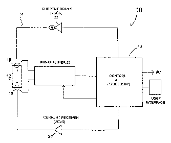
One preferred embodiment of the invention will now be described. Referring to
FIG. 1A, a tester 10 develops a time varying polarization voltage across
Device Under Test
12, and detects, measures and processes the polarization voltage. DUT 12
conventionally
3o has two electrical terminals, which are hereinafter designated as positive
terminal 16 and
negative terminal 18. Current signal 14 is imposed across DUT 12 by current
driver 22.
Current driver 22 may include conventional components. In one implementation,
current
driver 22 comprises a voltage controlled current source, although other types
of controlled
is
CA 02526491 2005-11-18
WO 2004/106946 PCT/US2004/015764
current source may be employed. In general, current driver 22 must be capable
of
producing a sustained bipolar current drive signal 14, which takes the form of
a precise
square wave. Current driver 22 is electrically connected to one terminal of
DUT 12. The
opposite terminal of DUT 12 is similarly connected to current 24, which may
incorporate a
voltage controlled voltage source. Current receiver 24 exhibits negligible
output impedance
(for all frequencies of interest, viz., including a sufficient number of high-
order harmonics
to properly define an edge corresponding to an abrupt amplitude transition),
so that it serves
as a vi~tuc~l AC g~our~d suitable for receiving the excitation current passing
through the DUT
from current driver 22. In the preferred embodiment, current receiver 24 is
preferably
to implemented as an active circuit element comprising a voltage controlled
voltage source,
but this active circuit element may be replaced by a direct connection, via an
electrically
conductive member, between the DUT and the common ground circuit of the test
system.
Preamplifier 30 also is connected across the terminals of DUT 12, which
preamplifier
senses, isolates, and amplifies the polarization voltage induced across the
internal
impedance of DUT 12 by drive signal current 14 supplied by driver 22. System
control,
data processing and I/O functions are provided by microprocessor 40, such as
an Intel
80386 processor, and associated analog and digital components; in an alternate
embodiment, some or all of these functions may be rendered in the form of
analog
computing and control circuitry. Furthermore, the excitation and sampling
parameters may
2o be adjusted according to control signals or commands received for either
Local Interface 44
or communications port 45 (FIG. 1B).
KELVIN CONNECTION AND SIGNAL DETECTION
Kelvin connection circuitry may be used to attach the components to the
device.
The Kelvin connection circuitry may include a first lead connected to the
controlled-current
source and configured for connection to the first terminal of the device, a
second lead
connected to the controlled-voltage source and configured for connection to
the second
terminal of the device, and third and fourth leads connected to the sensor and
configured to
be connected to, respectively, the first and second terminals of the device.
This apparatus
configuration is now described in detail.
3o In FIG. 1A, DUT 12 is connected to the tester 10 using four electrically
conduction
members (e.g., test leads) connected so that each lead malces an individual
connection
directly to the appropriate terminal of the device 12; thus, each connection
to current driver
22, current receiver 24, and preamplifier 30 are effected through separate
circuits. This
19
CA 02526491 2005-11-18
WO 2004/106946 PCT/US2004/015764
connection method, lalown as a Kelvin connection, reduces the interaction
between the
driving circuitry (i.e., current driver 22, current receiver 24, and their
associated connection
leads) and the sensing circuitry (i.e., preamplifier 30 and its associated
connection leads).
By virtue of the direct connection of the preamplifier test leads to the
terminals of device
12, and the relatively high input impedance of preamplifier 30, no drive
current flows
through any part of the sensing circuitry comprising preamplifier 30, so that
the detected
polarization voltage is completely attributable to response elicited in DUT 12
by the
excitation. Referring to FIG. 1B, detection and analog processing of the
polarization
response signal is provided by preamplifier 30, which may include four
operational
to amplifiers 54, 56, 58 and 64 to accomplish voltage sensing, DC offset
compensation, and
amplification functions of the preamplifier 30. Terminals 16 and 18 of DUT 12
are
electrically connected to respective positive and negative 'inputs of
instrumentation
amplifier 54, which may tale the form of a differential amplifier having a
very high
impedance, unity gain, and excellent common mode rejection. The output, signal
55,
produced by instrumentation amplifier 54 is equal (or , if amplifier has other
than unit gain,
is linearly proportional) to the potential difference between the inputs of
the amplifier 54.
When device 12 is an electrochemical cell or battery of cells having an
intrinsic DC bias
potential of its own, signal 55 will initially comprise the smn of this DC
bias potential plus a
polarization voltage component that is developed across the internal impedance
of DUT 12
by drive current 14.
Because the signal of interest is only the relatively small polarization
voltage
component of the full measured device potential, it is useful to remove the
effects of my
DC bias component from the output of preamplifier 30. This is accomplished
using an
offset generator 50 that supplies a suitable DC offsetting voltage signal 52
to an inveuing
scaling amplifier 64. Summing amplifier 56 combines the invented offset
voltage produced
by scaling amplifier 64 with signal 55 to produce signal 57; by this means,
the effect of the
DUT's bias voltage are removed from signal 57, so that it corresponds to only
the
polarization voltage component of the full potential appearing across DUT 12.
In the
embodiment depicted in Fig 1B, the value of the offset voltage is ultimately
determined by
3o microprocessor 40, which controls D/A 1 (a digital to analog converter)
that in turn controls
DC Offset Voltage Generator 50.
As noted, preamplifier 30 provides an output signal 55 substantially equal to
the
total potential present between the terminals of device 12. This output is
conveyed to a low-
CA 02526491 2005-11-18
WO 2004/106946 PCT/US2004/015764
pass filter 60 that is configured to remove higher frequency components from
the signal 55
to provide a filtered DC voltage 61 to a multiplexer (MUX) 62. The
microprocessor 40
controls the MUX 62 to route this signal to an A/D converter 64 that in turn
conveys a
digital representation of the signal 61 to microprocessor 40. The
microprocessor then issues
digital commands to offset voltage generator 50, which may include a digitally-
controlled
voltage source. Offset voltage generator 50 responds by providing offsetting
voltage 52
having a mag~litude equal to one half of the DC potential present across DUT
12, and
having the same relative polarity as terminal 18 of device 12.
Offsetting signal 52 is conveyed to scaling amplifier 64, which amplifies this
signal
l0 by a factor of negative two to produce output 65 that, by virtue of the
microprocessor's
program, equals the DC component of signal 55 in magnitude, but is of opposite
polarity.
As noted, signals 55 and 65 are conveyed to summing amplifier 56, which sums
them to
produce signal 57. This, in effect, subtracts the DC bias component 65 from
signal 55 to
remove the DC component associated with any intrinsic DC potential present in
device 12
and thereby isolate the polarization voltage component as signal 57. Signal 57
is thereafter
provided to the input of a high gain amplifier 58, which has an amplification
factor of about
1500, to produce polarization voltage output 32 that represents the signal of
interest in a
form conveniently used by digital and analog instruments.
Signal 32 is conveyed to unity gain buffer 37 that provides an isolated output
for test
bed instnunentation, such as an oscilloscope or other visual display device.
The buffer
prevents interaction between preamplifier 30 and the analog instrumentation
38.
DIGITIZATION OF POLARIZATION SIGNAL
Signal 32, representing the isolated and amplified polarization voltage, is
supplied to
A/D converter 34 that converts analog signal 32 into digital signal 36
comprising a series of
digital samples. Converter 34 is controlled by microprocessor 40, which
forwards clock
signal 42 to the converter, which is commanded to acquire a sample of its
input, signal 32,
during each clock cycle. Each digital sample substantially represents the
instantaneous
value of signal 32 at a point in time corresponding to a clock pulse. Digital
signal 36 is
passed to microprocessor 40 for processing, storage and, as required, for
transmission via
3o serial port 45.
AUTO CENTERING / AUTO POLARITY FUNCTION
21
CA 02526491 2005-11-18
WO 2004/106946 PCT/US2004/015764
Offset signal 52 is also used to provide a self centering effect. Signal 52
constitutes
the input signal to cmTent receiver 24, and, as noted above, is set by
microprocessor 40 to
have one half the magnitude of the DC bias voltage of DUT 12 with the same
relative
polarity. A primary attribute of the current receiver 24 is that its output
voltage is
maintained at a level equal to its input voltage, irrespective of the output
load current. This
means that terminal 18 of device 12, which is connected to current receiver
24, will be
maintained at a voltage equal to one half of the total DC bias of device 12,
having a polarity
equal in sign to the actual polarity of terminal 18 of device 12, as
determined previously by
the microprocessor 40. Because the output of current receiver 24 exhibits a
very small
1o impedance, its output voltage appears as a virtual ground, such that it
does not exhibit any
variations due to the reception of the time-varying excitation current
received through DUT
12.
Terminal 16 of DUT12 is electrically connected to current driver 22, which is
a
voltage controlled current source exhibiting very high output impedance. As
such, the
output of current driver 22 will assume whatever voltage potential, with
respect to the
relative potential of DUT 12, is required to ensure delivery of the proper
output current as is
functionally determined by its controlling input signal 21. Thus, by employing
both virtual
ground current receiver 24 that maintains at its output a DC potential
determined by the
microprocessor, along with a highly compliant current driver 22, the DC bias
voltage
presented by the DUT 12 is, in effect, centered with respect to local signal
ground, as shown
in FIG. 2. For example, if DUT 12 has a DC bias voltage of six volts, the
positive terminal
16 of DUT 12, which is comlected to current driver 22, will be three volts
above ground,
while conversely, its negative terminal 18 will be tln-ee volts below ground.
This self
centering capability offers great advantages for portable implementations that
operate using
2s a battery pack power supply. By ensuring that the cell voltage will be
centered about signal
ground, the total battery pacl~ voltage that is necessary to ensure proper
operation of the
electronic circuitry is thereby minimized. Furthermore, this arrangement males
the relative
polarity of the connections between the test system and the terminals of DUT
12 irrelevaazt,
provided only that siy als 14 and X1 are corrected to one terminal of the DUT
and signals
18 and X2 are comiected to the other teiTninal. Thus, if device 12 is attached
to the system
with its negative terminal 18 connected to current driver 22 and its positive
terminal 16
connected to current receiver 24, the control loop described by preamplifier
30, low pass
filter 60, multiplexer 62 A/D converter 64, and microprocessor 40, will
produce an offset
22
CA 02526491 2005-11-18
WO 2004/106946 PCT/US2004/015764
voltage signal 52 of the same polarity as terminal 16 of DUT 12. That signal
serves as the
input to current receiver 24, which then presents that voltage and polarity
back to DUT 12,
properly matching the polarity of DUT 12 and thereby centering the DC bias
voltage of
DUT 12 about the local signal ground.
GENERATION OF THE EXCITATION SIGNAL
Control signal 21 for current driver 22 is provided by Waveform Generator 48,
under control of the microprocessor 40. The control signal takes the form of a
precise
square wave voltage signal having several important characteristics, as
depicted in FIG. 3.
A primary characteristic of this signal is that is exhibits symmetry about the
horizontal
to (time) axis. As indicated in FIG. 3, a single cycle of signal 14 may be
subdivided into two
distinct half periods of equal duration. The positive half period from To to
Tl and the
negative half period from T~ to TZ must be of equal and constant duration for
each full cycle
of the wavefonn. By ensuring that the duty cycle of each square wave is 50%,
accurate
charge balancing will be achieved over the course of each waveform cycle, and
additionally,
the half cycle timing variance (skew plus fitter) within a whole cycle should
preferably not
exceed 20 nanoseconds. Similarly, the signal magnitudes during each half of
single cycle
must be equal. By ensuring synmetry both in the amplitude and time domains,
the galvanic
excitation provided to DUT 12 will have a net DC current value of zero when
summed over
an integral number of cycles. The amplitude and the frequency of signal 14 may
take on a
number of different values, but to ensure that the drive signal does not
significantly alter the
state of charge of DUT 12, the ampliW de is advantageously set so that the
peals to peals
value of the polarization voltage produced across device 12 does not exceed
several
millivolts per individual cell (viz., the excitation is adjusted to be
sufficiently small to
ensure that no irreversible reactions occur within the cell during a test
event), and
furthermore that precisely an integral number of cycles are generated at each
specific
frequency. To ensure detection of a very fast process or phenomenon within DUT
12, it is
necessary that the rise time of the square wave drive current exceed, by a
substantial
margin, the response time of the fastest process to be detected; otherwise,
the measured
response will reflect only the properties of the driving signal and circuitry,
not those of the
3o device under test. Hence, it is preferred that the square wave rise time be
on the order of
one microsecond, in order to ensure that an accurate and measurable
polarization response
is created.
23
CA 02526491 2005-11-18
WO 2004/106946 PCT/US2004/015764
To allow direct determination of ciuz-ent output of current driver 22, current
sensing
resistor 23 is connected in series with the output of current driver 22. The
drive current
passes through this resistor, developing a proportional voltage, which is
detected by
differential input current sense amplifier 25, whose output 27 connects to
multiplexer 64,
which is under the control of microprocessor 40. At various times, the
multiplexer may be
switched to route current sense signal 27 into A/D converter 64, whereupon the
digitally
sampled drive current information is conveyed to the microprocessor for
processing and
storage.
MICROPROCESSOR FUNTIONS
Microprocessor 40 is a stored program microprocessor commercially available
such
as the W tel 80386 processor; however, the use of other microprocessor types
is
contemplated for specific applications. Microprocessor 40 provides outputs to,
and accepts
inputs from, user interface 44 which may include a l~eypad and visual display.
Microprocessor 40 is further provided with a standard serial interface 45 to
permit data
exchange between the system and an external computer or other digital device.
Microprocessor 40 is responsible for overseeing and managing the operation of
the overall
system. Microprocessor 40 may also be provided with random access memory 46 of
conventional design, and other supporting devices as well, to permit the
storage and
manipulation of user inputs, data and outputs.
2o METHOD VARIANT #2
Variations on the circuit of FIG. 1B, representing alternate embodiments of
the
inventive apparatus, are provided in FIGS. 1C and 1D. FIG. 1C illustrates a
variation in
which preamplifier 30 is implemented using a four input instrumentation
amplifier. FIG.
1D illustrates an implementation in which the microprocessor no longer
provides control for
the self centering function; instead, novel analog circuitry is incorporated
within the
preamplifier itself whereby self centering may be achieved.
In the implementation of FIG. 1C, the DC offset voltage generator 50 develops
two
voltage signal outputs 52, 53 in response to an analog input control signal.
These outputs
are each equal in magnitude to one half of the magnitude represented by the
input control
signal, but are of opposite polarity (e.g., VouTl = (+V~ /2); VoUTa = (-Virr
/2) ). In this
variant, preamplifier 30 is equipped with four voltage input terminals and one
output
terminal, the first two inputs (designated A and B) are of a non-inverting
sense with respect
24
CA 02526491 2005-11-18
WO 2004/106946 PCT/US2004/015764
to the output signal, and the second two inputs (designated C and D) are of an
inverting
sense with respect to the output signal. The output signal is a voltage that
includes a highly
amplified copy of the algebraic sum of the four input voltage signals (i.e.,
VouT = lc(A+B-C-
D) ).
Microprocessor 40 may commence a preprogrammed sequence of operations, either
as a result of a user input command, or (in the case of an automatic
instrument embodiment)
as a result of detecting a change in the voltage present across the two
preamplifier input
circuits. Such a voltage change signals the completion of a suitable
connection to an
external device under test.
to The preprogrammed sequence may have an initial function of providing a
proper
control signal to a DC offset generator so as to null out the effect on the
preamplifier's
output due to the bias voltage present across the terminals of the DUT, and to
center the bias
potential exhibited by the DUT about local analog ground. This may be achieved
as
follows. First, the controller receives a sense signal, via analog-to-digital
converter 34, that
is representative of the voltage output of the preamplifier and is of the same
polarity, but
substantially amplified in magnitude, as the potential present across the
externally
connected preamplifier input circuits, due to the intrinsic bias of the DUT.
Next, in
response to this sense signal, the controller, via a digital-to analog
converter 49 (D/A 1),
commences outputting a constantly increasing control signal to the DC offset
generator.
2o The control signal has the same relative polarity as the output of the
preamplifier, and
continues to increase in magnitude as long as the output of the preamplifier
is other than
zero. In effect, this represents the behavior of an ideal non-inverting
integrator. The output
of the DAC is conveyed to the input of the DC offset voltage generator. The DC
offset
voltage generator is provided with two outputs having absolute mag~iitudes
that are always
the same and equal to one half of the magnitude of the controlling signal, but
are possessed
of opposite relative polarity. The negative output, of opposite polarity to
the generator
input, provides the controlling input to the current receiver. Both outputs
are connected to
the preamplifier, such that the positive output is connected to preamplifier
input, which has
an inverting sense, and the negative output, of opposite polarity to the
generator input, is
3o connected to preamplifier input, which has a non-inverting sense. Thus,
provided the
voltages presented by the DC offset generator will algebraically cancel the
voltage
presented by the device under test, the DC potential of the preamplifier
output will be zero.
CA 02526491 2005-11-18
WO 2004/106946 PCT/US2004/015764
If for example, the DUT is connected so that its positive terminal is
connected to
both the current driver and the positive input of the preamplifier input, and
conversely, its
negative terminal is connected to the current receiver and the negative input
of the
preamplifier, the output voltage of the current receiver will be seen to
become increasingly
negative (in response to the control signal emitted by the microprocessor)
with the passage
of time, forcing the DUT's negative terminal, which was initially at ground
when the test
event was commenced, to assume an increasingly negative value. Note that the
positive
terminal of the DUT is connected to two high impedance nodes (e.g., a high
impedance
preamplifier input and a high impedance current source). As such, though the
intrinsic bias
l0 potential of the device tinder test remains constant, the relative
potential of its positive
terminal will appear to become increasingly negative with respect to the
ground potential of
the overall circuitry.
The output of D/A 1 49 will continue to slew until the voltage presented at
the
output of the current receiver, as provided by the DC offset generator, is
equal in magnitude
to one half of the intrinsic bias potential of the DUT, and of the proper
polarity such that the
algebraic sum of the four preamplifier inputs will be precisely zero, leading
to a
preamplifier DC output of zero. At that point, the input to the non-inverting
integrator
(which in this embodiment is not present as a discrete circuit constituent,
but is instead
simulated by the operation of the microprocessor response to the output of the
preamplifier)
becomes zero, and accordingly, the output of the simulator integrator ceases
to change.
This in ttu-n causes the dewing of the output of D/A 1 to cease.
The net effect of this differentially configured integrator servo control loop
is
twofold. First, regardless of the actual connection of the test leads,
provided they are
connected in the proper pairwise fashion as previously noted, the loop action
will cause the
bias potential of the device under test to be precisely centered about local
analog ground.
Second, the DC bias of the device under test with respect to the
preamplifier's output
effectively becomes nulled out, allowing very small polarization signals,
present
differentially across the terminals of the DUT, to be highly amplified by the
preamplifier
and still appear centered within its effective output dynamic range.
3o This technique has the further benefit of allowing a substantial decrease
in the
required power supply voltages (with the attendant decrease in cost, and in
the case of
portable embodiments, a substantial decrease in size and weight) which are
required to
accommodate a device under test of given bias potential, as compared to
traditional DC
26
CA 02526491 2005-11-18
WO 2004/106946 PCT/US2004/015764
coupled methods wherein the relative potential of one terminal of the DUT
remains fixed at
relative ground, while the other terminal may appear either above or below
ground by an
amount equal to the relative bias voltage, depending on the polarity of the
test lead
connections. Of course, the problem of polarity could be simply avoided by
employing
capacitive coupling teclnuques, but this severely affects the accuracy of any
measurement at
low frequencies. Specifically, it renders measurement impossible for
excitation signals
characterized by relatively long duration half cycles of constant amplitude,
each of which
half cycles represents a temporary DC signal condition that cannot be properly
detected via
a capacitively coupled sensing means.
to The offset generator may be configured to provide either a fixed DC
offsetting
signal or a tracking DC offsetting signal. The signals output by the offset
generator may
then either be held at a fixed value (representing fixed DC bias offsetting)
throughout the
duration of a test event, or may vary (representing a tracking DC bias
offsetting method)
under control of the microprocessor (as it varies the output provided by its
embedded virtual
integrator) during the test event. This latter method allows the test device
to compensate for
changes in the bias voltage of the DUT caused by charging or discharging
currents from
some external source, or as a result of any other long-term variation in the
bias potential of
the DUT. Suitable algorithmic corrections can be applied to the polarization
voltage data to
compensate for the distortions created in the polarization voltage data as a
consequence of
2o the bias traclcing operation.
In the implementation of FIG. 1D, a variant is depicted wherein the bias
generator
function, that provides the DC offsetting capability, is incorporated within
the analog
circuitry of the preamplifier itself. Resistors 81 and 82 are optional, and
may be installed if
desired to provide bias currents to, buffers 83 and 84. Buffers 83 and 84 are
unity gain
amplifiers that exhibit high input impedance so as not to load, or draw
current from, DUT
12. Resistors 85-88 may have values of about 2000 ohms, with values matched to
within
0.01 percent to provide adequate common mode rejection; this can be readily
achieved with
monolithic resistor networks (suitable trimming resistors may be used as well,
to mitigate
the tight tolerance specification). Amplifier 90 is of the high gain
instrumentation type,
3o having high impedance inputs. Amplifiers 93 and 96 constitute with their
associated
componentry (particularly with respect to resistors 94 and 95, which are very
well matched
so that amplifier 96 behaves as a highly accurate unity gain inverter) a
differential output
integrator, having the known characteristic that its outputs will remain
constant provided its
27
CA 02526491 2005-11-18
WO 2004/106946 PCT/US2004/015764
differential input is zero. The differential integrator outputs are connected
to resistors 87
and 88, in a manner that the integrator outputs will automatically adjust to
force the net DC
value of the preamplifier output to always maintain a zero value (that is, be
always equal to
the potential provided at the non-inverting inputs of amplifier 93 and
amplifier 96). The
time constant of the integrator comprising elements 91, 92 and 93, is set by
the product of
resistor 91 and capacitor 92, and must be adjusted so that the lowest input
frequencies of
interest are not substantially attenuated. In an alternate configuration, tlus
time constant
may be made adjustable under external control, as, for example, by the use of
a digitally
controlled resistance element in place of resistor 91, to properly accommodate
any change
l0 in the intrinsic voltage of DUT (which, for example, could be due to the
fact that DUT is
being charged or discharged during the test event).
DESCRIPTION OF SYNCHRONOUS SAMPLING METHOD AND ANALYSIS
ALGORITHMS
Polarization voltage signal 32, depicted schematically in FIGS. 3 and 4,
represents
the voltage response developed across a typical electrochemical DUT by the
square-wave
drive current. Because the drive current signal is symmetric and periodic, and
of
sufficiently small amplitude to ensure linear response in the DUT, the
resultant polarization
voltage will exhibit similar syrmnetries. In most cases of interest,
particularly for
electrochemical accmnulators, the polarization response exhibits several
recurring
2o characteristics. At time To, corresponding to the abrupt positive
transition of the drive
current, the polarization response undergoes a similarly rapid change. Due to
the very short
rise time of the square wave drive current, this stepwise change of the
response accurately
represents a (nominally) time-invariant part of the polarization voltage, and
is therefore
attributable to the value of the ohmic (that is, r~ea~ component of the
device's impedance,
which is easily calculated from the known excitation current and the magnitude
of the
observed voltage step by the formula R = E / I. When this values is computed
for an
electrochemical accmnulator represented by an energy storage cell or battery,
it is
commonly referred to as the "resistance" of the cell/battery.
From a physical perspective, this resistance comprises several components that
appear arrayed as elements of a series connected electric circuit, which
elements may, for
example, include the actual resistance presented by the interconnecting
conductors within
the cell, the effective resistance presented across the thiclcness of the
active material region
on the electrode surfaces, and finally, the effective electrical resistance
attributable to the
2s
CA 02526491 2005-11-18
WO 2004/106946 PCT/US2004/015764
electrolyte within the cell. For many chemistries, these resistive components
change only
slowly throughout the life of a cell and exhibit a 'locally constant' value
(at a given point in
the cell's life) that is substantially unaffected by the cell's state of
charge; for other
chemistries, notably lead-acid, the apparent resistance of a cell is strongly
(and often
monotonically) related to the cell's state of charge, such that this
resistance value may
exhibit a substantial increase as the cell approaches a discharged state. In
light of these
clarification, it should be understood that when a cell is stimulated with a
current step, the
abrupt voltage step observed is characterized as time-invariant specifically
with respect to
the time scale of the current step itself, which is assumed to be much shorter
than the time
to required to make any significant change in the cell's state of charge,
since it is lcnown that
the value of this resistance may change appreciably for certain chemistries as
a function of
state of charge, and may therefore be used as one parameter in cell analysis
algorithms. It
should also be observed that an often overlooked component (and sometimes
quite
significant) of the real resistive component observed for a cell under test is
the resistance
1s attributable to the test connections themselves; in a real-world battery
application, this type
of resistive component is refewed to as the terminal connection resistance. If
this resistance
becomes excessive, the operation of a real-world system can become
compromised. It
becomes quite useful, therefore, to be able to immediately determine the cell
resistance
using the inventive method, by measuring the polarization voltage response
developed
2o across a sub-system comprising a cell plus at least one of its terminal
connections, and
extracting the time-invariant component of the response.
As can be seen in the figures, there may also be a small overshoot in the
observed
polarization voltage response, due to the combined inductive characteristics
of the DUT and
the test fixturing itself. Proper attention to fixturing will reduce stray
inductances to
2s negligible levels and allow the DUT's own inductive response (which
typically lasts from
one to several hundred microseconds) to predominate.
Immediately following the decay of any inductive overshoot and for the
remainder
of the half cycle, the response is seen to increase monotonically in magnitude
in a non-
linear fashion (unless the device appears purely resistive, leading to a
simple flat topped
3o square wave response). In particular, the slope (first derivative) of this
curved response is
seen to progressively decrease throughout each half period, and is
recognizable as being
similar to the well lcnown exponential function (1- a lit), which is used to
describe electrical
29
CA 02526491 2005-11-18
WO 2004/106946 PCT/US2004/015764
circuits containing resistive and capacitive elements. This curved poution
will hereinafter be
referred to as the time-varying component of the polarization response.
It is often useful to take the value of the excitation cmTent (which is by
assumption
held constant throughout the flat topped portion of an excitation half cycle
or pulse) along
with each instantaneous (that is, discretely sampled) value of the time-
varying component of
the polarization voltage (that is, as distinct from the time invariant
component defined
above) and compute, by a direct application of Ohm's Law, a set of values for
the apparent
polaf-ization resistance as it evolves during the flat-topped excitation
portion; these
computed values may be used as parameters in cell analysis algorithms. It will
be apparent
to as well, that such algoritluns might include computations, using pairs of
values, of the rate
of change of the polarization resistance, (APR / fit), which computed values
may in turn be
used to estimate various battery indicators such as state of charge and state
of health, and be
used to identify specific fault conditions. A precipitous amplitude change in
the response
signal that is not correlated with a simultaneous abnipt change in the
excitation can be
indicative of the creation of (or the dissolution of) a spurious low impedance
connection
such as a 'whisker' or metallic dendrite across a normally highly-resistive
interface region
within a cell.
A plot of the of the time-varying component of the polarization voltage as it
evolves
during the constant portion of a current pulse is often observed to exhibit at
least two
2o distinct regions, arising from processes having widely different
characteristic time
constants. These portions are identified in FIG. 4B as the fast (74) and slow
(75) processes,
respectively, and exhibit commensurately differing curvature. Fast processes
tena to
expend themselves in the early part of each half cycle, while the later tail
section takes its
shape from slow processes and so changes relatively gradually over time.
At T1, the next stepwise current transition occurs, whereupon a polarization
curve of
similar shape appears, belt now tending downward. Provided that neither the
condition nor
state of charge of the DUT changes appreciably during several consecutive
excitation
periods (i.e., the square wave cycles), it is apparent that the shape and size
of overall
response waveform will also remain relatively constant. In general, the
polarization voltage
signal is well behaved and, except for a discontinuity at each stepwise edge
transition, is
continuous.
CA 02526491 2005-11-18
WO 2004/106946 PCT/US2004/015764
The polarization response is digitized by converter 34, according to a
sampling
schedule controlled by the microprocessor 40, and synchronized with the
excitation. To
accurately capture all the details of an arbitrary wavefonn, digital sampling
theory teaches
that the sampling rate must be at least twice as high as the highest frequency
component of
interest to avoid aliasing errors, and in practice, ten-times oversampling is
used to ensure
the fidelity of the digitized waveform.
Conventional digitization techniques employ a fixed interval sampling schedule
(e.g., the time interval dt between samples remains constant throughout a test
event)
wherein the analog wave form is repeatedly sampled and digitized,
synchronously with a
to sample clock control signal having a constant frequency (f = 1/ 8t). As is
well known to
practitioners of the art, constant 8t sampling is preferred if the data is to
be analyzed using
discrete transforms (Laplace or Fourier). The attainable resolution of such
transform
analyses is limited by the magnitude of bt, in that decreasing 8t (that is,
increasing the
sampling rate) allows faster processes, or equivalently, higher component
frequencies, to be
resolved. Since typical electrochemical cells often exhibit transient
responses in the
microsecond range, particularly when excited by a square wave current (i.e.,
galvanodynamic excitation), it would appear that a very high sampling rate is
preferred.
Furthermore, when testing electrochemical accumulators whose behavior is
governed in part
by relatively slow kinetic processes such as diffusion, a very low frequency
square wave
2o excitation (0.1 and 0.01 Hertz) is required to elicit a significant
polarization response.
When such a slow waveform is repetitively sampled at a high rate, a very
substantial
number of digitized values will be accumulated, especially if the test
procedure includes
many cycles of the waveform to ensure adequate noise averaging, or to validate
the
assumption of invariance over repeated cycles. For many applications,
particularly low cost
commercial or portable device embodiments, the burden of raw data storage alld
management presented by such a large data set may be prohibitive.
Although constant 8t sampling may be desirable and necessary for certain
analytical
transform methods, a valuable aspect of the present invention is the use of
novel non-linear
sampling schedules whereby 8t is progressively increased for each successive
sample
3o acquired during each half cycle. By convention, fast processes are those
that run to
completion within the first few tens of milliseconds of each half cycle. To
capture the
details characterizing these early, rapidly evolving events, fast sampling is
surely necessary.
31
CA 02526491 2005-11-18
WO 2004/106946 PCT/US2004/015764
Conversely, there are other slower processes having responses that evolve over
a
time scale of many seconds. These are manifest in the tail section of the
response waveform
with its much gentler slope and commensurately diminished high frequency
content, thus
allowing a substantially relaxed sampling schedule to be employed without
sacrificing any
measurement accuracy.
Therefore, when the actual time domain response of the evolving polarization
voltage is of interest, a non-linear sampling schedule can be prescribed
whereby the inter-
sample time is progressively increased in a particular fashion throughout each
half cycle.
Excellent resolution is achieved for both the early/ fast and later/slower
polarization
to processes, with a total accmnulation of far fewer actual data points as
compared to the
conventional constant ~t sampling paradigm.
One preferred non-linear sampling sequence is based on a geometrically
increasing
series of inter-sample delay times 8t;, each of which represents an integral
number of base
clock periods, OTCI~It, which base clock is derived from a separate fixed
frequency
oscillator, preferably operating at one megahertz or higher. One useful
algorithm for
generating an appropriate series of sample events is based on an exponential
relationship,
wherein 8t; represents the time delay between the abrupt step corresponding to
the
beginning of a half cycle and the i th designated sampling point:
8t; _ [~TcLx] x [I~~a~]. I~ = constant, a is a member of a set of values
2o To create the simplest type of sampling schedule whereby N geometrically
spaced
samples will be acquired during each half cycle, a set of ascending values for
a is provided,
{ ai ~ for i=0 to N, where i represents the index of a sample delay value, for
example at =
{0, 1, 2, 3, . . . . , N}, and N is made equal to 2.
When the formula is applied to this set, the sampling sequence will appear as
a
simple exponential series of N+1 time delays, each of which is an integral
multiple of the
base cloclc period ~T~L,c. Moreover, the ratio between any adjacent pair of
time delay
values is be precisely 2, so that the entire set of time delays corresponds to
a geometric
series; if the base clock is set to 1000 Hz, then ~T~LK = 1 millisecond,
yielding series f 1 ms
(delay of first sample from step), 2 ms, 4 ms, 8 ms . . . }. In some cases, it
is useful to
3o establish a sampling schedule with finer granularity by allowing K to
assume a value that
corresponds to a fractional power of 2, like 2~x and so on. Since, in this
case, the resultant
series produced by the formula will no longer comprise only whole numbers (the
square
32
CA 02526491 2005-11-18
WO 2004/106946 PCT/US2004/015764
root of 2 has an infinitely repeating fractional component), a rounding method
must be used,
whereby the a~ values are rounded off to the nest higher (or lower) integer,
since by
assumption, it is not allowed to specify a sampling schedule that contains 8t;
values that are
not integer multiples of the base clock.
Moreover, in some cases, it may be preferred adjust the scheduled time delays
for, or
completely omit, the first few samples in each series, particularly to avoid
the peals caused
by the inductive behavior of the DUT or the test fixture. By appropriate
selection of the
parameters, a series can be constructed which provides many closely spaced
samples during
the early part of the polarization waveform where fast events occur, with
fewer samples
to later on as the rate of change of the polarization voltage is diminishing.
By resetting i to
zero at each stepwise transition and then incrementing again to N, an
identical sampling
schedule is generated for each half period, greatly simplifying later
analysis. FIG. 5A
shows a typical polarization waveforn, with seven sampled data points in each
half cycle,
representing an exponential sampling schedule [S1 , i = f 0 to 6)].
1. First Transformation Step: Graphic Normalization & Averaging
Once the sampled data is collected, a normalization transformation may be
performed, whereby the time varying portion of the response is separated from
the step-wise
abrupt transition that defines the beginning of the half cycle. This
transformation may be
applied to either uniformly or non-linearly sampled data. Referring to FIG. 5,
the
polarization voltage value of sample So (at time To), being the first sample
following the
transition, is used as a reference value, and is normalized by convention to a
value of zero,
as shown in FIG. 5B. The actual voltage difference between sample So and S1 is
then
calculated from the raw data and used as the y-value for S1 in FIG. 5B;
successive samples
are treated similarly, leading to an upward tending curve that intersects the
x-axis at time To.
The magnitude of the difference, designated ~Eo, between sample So and the
final sample
from the preceding half cycle represents the size of the step. In FIG. 5B, the
magntude E
of the step is plotted immediately to the left of sample point So, at time T~.
In the graph, a
line is shown connecting points S~ and So. In fact, the transition of the
polarization voltage
between these points is very rapid, and so that point S6, if plotted according
to the time scale
used for all the other sample points, would appear almost directly above point
So. To
facilitate interpretation of the graphic data in FIG. 5B, point S~ has been
shifted slightly to
the left and a coimecting line drawn to point So.
33
CA 02526491 2005-11-18
WO 2004/106946 PCT/US2004/015764
This transformation is applied individually to the data from each half cycle,
resulting in a set of vectors each containing N+2 elements (that is, samples
So to SN, plus the
DEo value). To ensure that the data contains no artifacts, the information
from the first two
half cycles (one complete square wave cycle) may be omitted from subsequent
analyses.
The remaining M vectors are then divided into two groups (corresponding to
positive and
negative half cycles, according to the sign of the excitation current) as
shown in FIG. 3A.
Each of these groups can be formally described as a two-dimensional matrix,
comprised of
M vectors, corresponding to the number of whole cycles used in the analysis,
containing
N+2 elements. Within each matrix, the values of coiTesponding elements are
added
to together and these sums are each divided by the number of vectors in the
matrix, yielding a
single N+2 element vector representing the mean value of all the vectors in
the matrix; these
are designated as the mean positive vector and the mean negative vector.
As is well known to practitioners of the art, such an averaging technique when
applied across M cycles of a periodic waveform serves to reduce the effect of
any random
noise signals present within the raw waveform data, by approximately a factor
of M1~2;
furthermore, the effective bandwidth of the signal is not limited.
Provided that the DUT is in an open-circuit state, and the internal chemical
reactions
behave reversibly for the small excitation signals employed (and do not
exhibit alzy
hysteresis effects), the shapes of the mean positive and mean negative vectors
will be mirror
2o images, reflected across the x-axis (time axis), specifically, when all the
sample values in
the mean negative vector are multiplied by minus one (hence, are normalized by
sign
inversion), the resultant inverted negative mean vector should perfectly match
the mean
positive vector. Any difference between these two sign-normalized vectors
indicates either
that state of the electrochemical system within the DUT has changed during the
data
acquisition period, or that the DUT was behaving in a nonlinear fashion as a
result of the
excitation itself. Provided that these mean vectors are congruent, they may be
averaged,
yielding a single vector characteristic of the device under test. A graphic
presentation of
these vectors is irmnediately useful for qualitative understanding of the
device's
performance and condition.
2. Second / Tliird Transformation Step: Linear to Log Time Axis
In the preferred embodiment, to further aid comprehension and understanding of
the
mean vector data, two additional transformations are undertaken. These require
either that
34
CA 02526491 2005-11-18
WO 2004/106946 PCT/US2004/015764
the data has been sampled according to an exponentially derived schedule, or
that evenly
sampled data has been re-sampled (or decimated) according to a similar
exponential rule. In
FIG. 6A, a typical positive-going mean vector is shown as a continuous curve,
with the
actual sampled data points indicated. The accompanying legend provides the
correspondence between each sample point (either identified by an integer
index or as ~Eo)
and its relative time of acquisition, in base clock periods, relative to the
step-wise transition.
The index values increment uniformly, while the time values increase
exponentially.
When the data is replotted using the integer index values as the x coordinate,
FIG.
6B results, now exhibiting a well-known logarithmic characteristic, due to the
fact that the
1o index of each point is directly proportional to the logarithm of its
associated time value, 8t1.
Note that each point in linear space finds correspondence with a unique point
in logarithmic
space. This transformation facilitates immediate visual identification of
curvature changes,
which signal the occurrence of underlying processes. Details of fast processes
are
sufficiently spread out to be readily apparent, while the portion of the graph
allotted to
slower processes is relatively compressed without loss of any important
information.
A further manipulation of the logaritlmnically transformed data is performed,
by
simply reflecting the curve about the vertical axis, as shown in FIG. 6C, and
translating it
horizontally so that the data point So, corresponding to the last element in
the mean vector,
becomes the y-intercept. These points are re-labeled in the graph, for
reasons, which now
become apparent.
In the preferred embodiment, the information of interest relates to the change
of
polarization voltage as it evolves during each half cycle of the excitation
current. Each
sampled data point is uniquely identified by an offset interval 8t;, measured
with respect to
the previous transition. It is useful to define a new quantity, the equivalent
polarization
frequency fP; corresponding to a specific sample point i, referred to
hereinafter as the
polarization frequency, which is equal to 1 / (2 x 8t;); where this value
represents the
fundamental frequency of the symmetric square wave comprising the two half
cycles each
of duration 8t;.
In this manner, the point associated with the lowest measured polarization
frequency
(that is, having the longest sampling delay interval with respect to its
corresponding step
transition) appears leftmost on the graph, with ascending frequencies proceed
to the right.
The graph is again logaritlmnically scaled with respect to polarization
frequency, such that
CA 02526491 2005-11-18
WO 2004/106946 PCT/US2004/015764
while the ratio of adjacent frequencies is constant, succeeding points are
uniformly spaced
along the x-axis. This manner of presentation, plotting polarization frequency
along the
abscissa, has been found to be more convenient and more easily understood by
those
familiar with the art. Viewing polarization response in terms of frequency
allows
immediate comparison to the vast amount of Frequency Response data available
in the
"Impedance Spectroscopy" literature.
The present invention supports qualitative and quantitative analysis of energy
cells.
FIG. 7A provides a typical polarization response of a fully charged lead-acid
cell. The
peak-to-pear magnitude of the response across the cell is preferably not
greater than several
to millivolts, to preserve linear response. FIG. 7B is the response of the
same cell, in a
discharged condition. Intermediate states of charge exhibit curves falling
between these two
extremes. At progressively higher charge states, the magnitude of ~Eo
decreases
monotonically, while the steepness, and hence the overall height of the
wavefonn,
increases. The twelve curves presented in FIG. 8 represent data from a single
12 volt lead-
acid automotive battery at different states of charge. The bold line
represents the mean
values of the sample population at full charge, while the others depict the
response of the
battery discharged and at ten ascending states of chaxge. This sequence
reflects the changes
produced by ten one hour charge events, each at the C/10 rate. For a fully
charged battery,
the curve appears steeply curved, with the polarization voltage increasing as
the polarization
2o frequency decreases. In the discharged state, the curve is nearly
horizontal, exhibiting at the
high frequency (right) end, a value approximately twice that of the charged
unit.
Intermediate charge values fall between these two curves.
METH~D VARIANT #3
As described previously, the DC offsetting signal may be adjusted to
acconnnodate
slow variations in the intrinsic bias voltage presented by a DUT whose
relative state of
charge is changing as a consequence of receiving either a charging or
discharging current
concurrently with the time-varying current excitation as prescribed by the
inventive method.
According to well-known principles of circuit theory, separate currents may be
surmised at a
circuit node, which node in this example corresponds to that terminal of the
DUT connected
to the current driver. During a simultaneous application of both a test
current signal and a
charging or discharging current signal to said DUT terminal, it is therefore
contemplated
that the time-varying polarization response component attributable to the test
current can be
36
CA 02526491 2005-11-18
WO 2004/106946 PCT/US2004/015764
isolated and analyzed, to provide real-time information regarding the state of
charge and
condition of the DUT.
When a DUT is connected to an operating external charger or discharger, the
test
method may therefore be applied ii2 situ while the DUT is being charged or
discharged,
respectively. In light of the fact that the excitation of the inventive device
may comprise
arbitrary waveforms, the device can be adjusted to perform both as a tester
and a
charger/discharger simply by modifying the excitation cmTent so that it
exhibits a suitable
DC or slowly varying offset current, which offset current represents the
desired charge or
discharge current value.
l0 Due to the fact that preferred test waveforms exhibit abrupt
discontinuities and may
be configured to appear as series of rectangular pulses (whose characteristics
may be
adjusted as needed), the test device may be effectively transformed into a
pulse-mode
charger (or discharger) by using an excitation that exhibits a net positive or
negative bias
and also contains a time-varying component suitably disposed for eliciting a
time-varying
polarization response that may be synchronously sampled to yield samples that
are analyzed
to provide an evaluation of at least one characteristic of said system.
Moreover, the diagnostic information obtained according to the method may be
used
to modulate the charging/discharging process to further improve its
performance.
Specifically, the sampled values (or the results of their analysis) may be
used in a closed-
loop topology (e.g., a feedback system), whereby modulation is effected for
certain
excitation characteristics including the net bias of the excitation (i.e., its
average value), and
the amplitude, duration or duty-cycle characteristics of the time varying
wavefonn
component of the excitation. By incorporating these variation into the
inventive apparatus,
it may be used in applications where the well-known the benefits of pulse-mode
charging,
such as reduced charging time, improved charging efficiency and remediation of
a variety
of cell deterioration mechanisms (e.g., sulfation in lead-acid cells), are
desired. An example
of such an improvement is now provided.
Predictable real-time variations in the peak-to-peak amplitude of the
polarization
response can be used to detect the end of charge condition in a lead-acid
battery. A constant
3o frequency square wave excitation (at 0.1 Hz) is preferred, and the response
is continuously
monitored throughout the charging process. Under dynamic conditions (charging
or
discharging), the offsetting voltage is continually adjusted to compensate for
the changing
37
CA 02526491 2005-11-18
WO 2004/106946 PCT/US2004/015764
potential of the device under test. As the battery approaches its fully
charged state, the
amplitude envelope (peak-to-peak value of polarization response) exhibits a
rapidly
increasing magnitude, indicating an increase in the Faradaic resistance
followed by the
onset of the oxygen evolution reaction as the polarization voltage reaches the
gassing point.
The response curve of a healthy cell will appear smoothly curved, with a
steeply sloped
onset, gradually tapering off to an asymptotic response (whose maximtun
amplitude is
proportional to charging current). In contrast, an unhealthy cell that has a
reduced level of
absorbed electrolyte, due for example to previous episodes of overcharging,
shows a
pronounced kneel in the curve: the rate of change of the polarization response
(its slope)
l0 abruptly assumes a lower value.
Two important factors are evident here, shown in FIGS. 9A and 9B. First, when
the
polarization response begins its precipitous rise, the cell has accepted all
the energy it can
for recharging so the energy is now going into electrolysis. At this point, it
is preferable to
discontinue charging, since further energy input is no longer increasing the
state-of charge,
but is merely generating gas and unnecessary heat. Second, the knee in the
curve is
indicative of a relative increase in the electrochemical depolarization
process occurring at
the negative plate, due to the increase availability of gaseous oxygen, which
has escaped
from the electrolyte and is diffusing directly to the negative plate. Thus,
the presence of
such a lcnee is symptomatic of cell dry out, that is, a depletion of
electrolyte, as is often
2o caused by excessive overcharge.
METHOD VARIANT #4
While most of the preferred excitation protocols comprise waveforms that
exhibit
abrupt discontinuities, there are occasions where the use of ctuvilinear
waveforms, such as
sine waves, is desirable; the use of sinusoidal excitation is encompassed
according to the
inventive method. While sine waves do not contain any abr~ipt transitions
thatnnay be used
to define a 'beginning' of each waveform, they do exhibit a particular
symmetry wherein
each cycle contains two evenly spaced zero-crossings, or alternatively, two
evenly spaced
amplitude maxima of opposing polarity. Either of these pairs of points (e.g.,
zero-crossing
or pealcs) may be conveniently defined as the 'beginnings' of the excitation
waveform part-
cycles, which beginning points may be used for the propose of establishing
sampling
synchronization. Note that in general, any convenient (and corresponding)
points within the
two consecutive half cycles of a sine way could be defined as the 'beginning'
points.
38
CA 02526491 2005-11-18
WO 2004/106946 PCT/US2004/015764
The use of synchronous sampling permits the point-by-point data averaging
techniques previously described to be employed, to achieve the known benefits
of noise
reduction without causing aaiy change in the frequency spectrum of the sampled
data (other
noise reduction methods such a Finite Impulse Response (FIR) filtering
inevitably lead to a
reduction in the bandwidth and phase shift of the filtered signal).
In some cases, however, a reduction in the bandwidth of the filtered signal
may be
precisely the desired result. A well-laiown example is afforded by the method
of
synchronous demodulation, whereby a periodic signal of interests is convolved
with (e.g.,
"multiplied by) a r eference cloclc signal, to yield a synchronously rectified
output of the
l0 signal of interest. If this rectified output is averaged (or integrated)
the resultant
(nominally) DC output signal is proportional to the cosine of the angle
between the
reference clock and the signal of interest, since by assumption, the signal of
interest is a
response signal produced in a DUT by an excitation, and hence both have the
same
fundamental frequency.
According to the present method, the response signal of the DUT is
synchronously
sampled, and therefore the digital data may be manipulated to yield an outcome
that is
formally equivalent to that produced by a conventional (i.e., analog circuit
implementation)
synchronous demodulator. A corollary, obvious to one skilled in the art, is
that by
performing both in-phase and quadrature detection (that is, IQ
derrtodulatiora) in the digital
domain, representative values for both the cosine and sine components,
respectively, of the
signal of interest may be calculated. The excitation represents a known
current, and the
response appears as a voltage, so these components represent the real and
imaginary parts of
the DUT's complex admittance, from which impedance values may be derived.
According
to well-established techniques, these admittance/impedance values may be
assigned to
elements of a well-formed equivalent circuit model.
METHOD VARIANT #5
A particularly useful class of excitations represent composite waveforms
comprising
the equivalent of a plurality of sine wave frequencies; such wavefonns may be
created
within the waveform generator component of the apparatus, and therefore the
relative
amplitude and phase relationships among these various sinusoidal components of
the
excitation are known a pf°iof°i. Provided that the response of
the DUT is acquired according
to the preferred synchronous sampling method, it is immediately possible, via
suitable well-
39
CA 02526491 2005-11-18
WO 2004/106946 PCT/US2004/015764
established analysis methods (e.g., the Fourier transform) to decompose the
response into a
plurality of vector components, each of which constitutes the amplitude and
phase values of
a particular frequency component. By this method, a mufti-tone test scheme may
be
directly implemented within the context of the inventive device. Furthermore,
conventional
harmonic distortion and intermodulation distortion analyses may be performed
on the
sampled data (that is, through the identification of any frequency components
in the
response signal that were not present in the excitation) to aid in the
characterization of the
performance of the DUT, and thereby accurately determine the nature of non-
linear
behaviors that can be correlated with, and hence will be descriptive of,
underlying electrical
l0 and electrochemical processes.
METHOD VARIANT #6
Another alternative embodiment relates to evaluating primary (single-use)
electrochemical cells. Here again, complex pulse-type current excitation
signals are applied
to the cell and concomitant time-varying cell polarization voltage data is
acquired. The
shape (i.e., the magnitude and curvature) of the curves obtained when the
polarization
voltage response is plotted as a function of time provides information about
the state or
characteristics of the cell. To assess the condition of an unknown cell, its
excitation-
response profiles) (time-series data) is obtained and evaluated in comparison
with
previously obtained benchmark data for the particular cell/battery type, via
loole-up table,
logic, or data processing algorithms. The results of this evaluation can be
presented either
with results displayed via an illuminated 'GO/NO-GO' indicator, or presented
quantitatively
as percent state-of charge, or with a specific indication of relative cell
health condition or
failure mode.
According to one embodiment disclosed above, a non-invasive test may be
accomplished by, a symmetric, bipolar square wave current (that is, of
alterlating positive
and negative sign) on an electrochemical cell (or battery of cells), and the
resultant time
dependant polarization voltage response is measured. To ensure that the
condition of the
cell is not substantially altered by the test itself, the excitation signal
current must be
properly adjusted to elicit only a very small peak-to-peak voltage response,
typically 0.1
of nominal open-circuit voltage of the cell. Due to the symmetry properties of
the
excitation (both in the time and amplitude domains) the net energy state of
the cell will not
be significantly affected by the test. Thus, such a test can be repeated many
times with
virtually identical results. Since the excitation signal is small by
assumption, is periodic,
CA 02526491 2005-11-18
WO 2004/106946 PCT/US2004/015764
and exhibits a constant peals-to-peak amplitude, the response will also
exhibit a constant
peak-to-peals amplitude response throughout the entire test protocol duration.
The
information contained in the response signal represents the actual time domain
response of
the electrochemical system, and may be manipulated (via suitable mathematical
transforms)
to yield frequency response information. In addition, values for the elements
of an
equivalent electronic circuit model can be calculated. Finally, the
characteristics of specific
electrochemical processes often can be derived directly from graphical
analysis of the time
domain response plots.
When it is desirable to test certain types of primary cells, it is often
preferable to
l0 modify the excitation: the symmetric, bipolar waveforms are replaced by
unipolar
waveforms that contain only discharging and zero-current (rest) events. An
illustrative
example of such an embodiment is now provided.
Testing the Lithium Sulfur Dioxide Primary Cell
Lithium sulfiu dioxide primary cells (LiS02) exhibit a 2.95V nominal operating
voltage and provide high energy density and a relatively flat discharge
profile over a wide
temperature range. This combination of low weight per watt and excellent
discharge
characteristics make them the cell of choice for mission critical
applications. The flat cell
voltage profile, which makes the cells desirable, also leads to difficulties
when it is used as
a metric for detemnining the cell's condition and state of charge.
The LiSO2 cell employs lithium as the anode and sulfur dioxide as the active
cathode material. The electrolyte is typically an organic solvent such as
acetonitrile
containing lithium bromide to provide ionic conductivity. During discharge,
the lithium is
oxidized to Li+1 to release an electron to the load circuit. Two lithium ions
then ",i~,-atP
toward the cathode area where they combine with two sulfur dioxide molecules,
along with
a pair of electrons (from the load via the cathode circuit), to form lithium
dithionate
(LiaS2O4). In cells where lithitun is the stoichiometrically limiting
electrode, discharge
terminates when all of the lithium is constuned. Otherwise, discharge ceases
when the
cathode becomes blocked by the precipitation of the discharge product.
When the LiSO2 cell is left in an open circuit condition, the discharge
reaction
proceeds directly at the anode, foaming a thin coating of lithium dithionate
that serves as a
highly effective passivation layer. This prevents further reaction and self
discharge, leading
to exceptional shelf life. After extended storage times the cell's terminal
voltage, when first
41
CA 02526491 2005-11-18
WO 2004/106946 PCT/US2004/015764
connected to a load, appears somewhat depressed (the 'voltage delay' effect).
As the
discharge current removes the passivation layer, the terminal voltage soon
recovers to its
expected value. It should be noted that the open circuit voltage of a fully
'passivated' cell
can rise more than 50 millivolts higher than its nominal value.
A fully charged cell can be expected to exhibit its nominal open circuit
terminal
voltage of about 2.95V. Upon connection to a load, the terminal voltage first
undergoes a
rapid drop, followed by a recovery during the next several minutes as it
climbs baclc to a
constant value determined by the load current. The value of the 'recovered'
terminal
voltage remains exceptionally constant for a given load cmTent throughout the
usefiil life of
to the cell. Upon cessation of the load current, the open circuit voltage
(OCV) will begin to
rise, eventually approaching the nominal value very closely. Thus, OCV is not
suitable as
an indicator of state of charge.
Synopsis of the Techninue
When it is desirable to quantitatively evaluate the state of charge of a LiS02
(single
use) cell/battery, an extension of the excitation-response method is employed.
A pulsed
unipolar excitation signal is employed, with the amplitude scaled up to ensure
a non-linear
"non" non-invasive response. W this case, both the wave shape as well as the
amplitude
envelope of the resultant polarization voltage response will vary as a
function of time, and
using these data conjointly allows an accurate determination of the
characteristics of cell
2o condition and state of charge.
The excitation signal (FIG. 10) is a 50% duty cycle rectangular square wave
current,
comprised of equal duration periods of constant discharge current and zero
current (e.g.,
open circuit), so that the average amplitude of the excitation waveform is
equal to one half
of its peals current value. A test protocol commences with alternations
between a discharge
pulse lasting ~t seconds, followed by a zero-current rest period of ~t
seconds, and so on, for
a number of repetitions, ending with a last rest period of ~t seconds. The
preferred duration
of these discharge pulses depends on the particular cell type tested, and must
be sufficiently
long to ensure polarization of the electrochemical interface. For example, the
pulse duration
may range from 0.1 to 5 seconds. The amplitude of the current is sufficiently
large to
produce a slight net discharge of the cell (about 0.1% of its nominal
capacity) Burin a
single test event comprising one or more excitation cycles. In practice,
suitable cmTent
42
CA 02526491 2005-11-18
WO 2004/106946 PCT/US2004/015764
levels fall between C i-nr-raceiz and C 1-hr-rate/8~ where C 1-hr-rate is the
nominal amp-hour
capacity of the cell.
The duration of each pulse is very well controlled (in a prototype test trait,
the
measured width variation between consecutive one second pulses was less than 2
nanoseconds, equivalent to 1/500 ppm), allowing synchronous data sampling
techniques to
be used. The cell's voltage during each charge pulse and rest pulse is sampled
under an
identical sampling schedule. Thus, for all pulses, the Nt~' sample in each
pulse is taken
precisely k microseconds after the begiming of the pulse. This allows
'equivalent' points in
consecutive pulses to be directly compared. FIG. 11A provides a plot of the
data obtained
in a typical test protocol comprising 255 consecutive discharge/rest cycles.
Of particular
importance are the overall wavefonn extrema (i.e., the maximum values of
positive and
negative excursions that occurred during each pulse event), which are readily
obtained by
this method. When the extrema points alone are plotted in FIG. 11B, the result
is the
afnplitucle envelope signatuf°e of the cell. Both the overall envelope
amplitude (that is, the
peak-to-peals cell voltage excursions) as well as the shape of each individual
response
waveform changes considerably during the course of the test protocol (see FIG.
11C and
11D). By direct inspection of this type of plot, the relative condition and
state of charge of
the cell can be estimated. Suitable algorithms, whose rules have been
established by
analyzing previously obtained baseline cell performance information (or
extracted by neural
2o network analysis, tlu-ough training on full range of 'charge state' data
from the target cell
type), can be employed to automate the measurement/analysis process. In
addition, detailed
analysis of the raw data provides considerable insight into the behavior of
the cell, and
allows individual electrochemical processes to be identified and precisely
quantified.
Description of a Precision Time Domain Spectrometer Device
The apparatus applies well-controlled current pulses to a Device Under Test.
To
permit observation of the fast electrochemical events that occur at the onset
of a current
pulse, the rise time of the current pulse is preferably made significantly
shorter than the
response time of the fastest process of interest. For example, a pulse rise
time on the order
of one microsecond may be used for small cells that exhibit low inductance.
For larger
3o cells, this criterion may be relaxed by at least an order of magnitude,
since the internal
inductance of large cells is significant and overwhelms the observable
response arising from
the very fast initial processes. To avoid errors, particularly when smaller
cells are tested,
the output, offset current should be no greater than 0.01% of the pulse
amplitude. The
43
CA 02526491 2005-11-18
WO 2004/106946 PCT/US2004/015764
current driver itself is preferably embodied as a precision voltage controlled
current source,
operating 'to ensure pulse shape accuracy in the neighborhood of zero current
(and during
any zero-crossings). When large cells are to be tested, a simple switched
current source
(e.g., a bipolar transistor with scaled emitter current-setting resistor) will
suffice, where the
inevitable errors (pulse overshoot or ringing) at turn-on and turn-off become
unimportant.
Pulse amplitude accuracy is ensured through the use of a low slew,
programmable
waveform generator that incorporates a very stable voltage reference. For
precision
laboratory applications, this reference should provide a very low noise
output, with less than
0.5 ppn~/degrees centigrade drift. For less demanding commercial applications,
this
to criterion may be relaxed by at least an order of magnitude. The pulse
amplitude is
parametrically adjustable, and can be changed to any value for each successive
pulse. This
feature is useful for cells, which require a substantial depolarizing event
(one or several
higher amplitude pulses) at the beginning of a test protocol.
Proper pulse generation for precision duration/sequence time is critical for
accurate
measurement. Nanosecond duty-cycle skew is achieved through the use of high-
speed logic
and sub-nanosecond, balanced analog switching techniques. Both pulse duration
and the
composition of the overall excitation sequence are programmable.
To measure the cell's response, a 16-bit high-speed analog-to-digital
converter is
employed. The sampling schedule may be either constant rate (fixed sampling
interval), or
2o parametric-by-pulse. In the latter case, each pulse is sampled according to
the same non-
linear schedule whereby the intersample time delay increases between
successive points: m
exponentially increasing series of sample intervals is preferred, but other
types of schedules
may be employed for specific applications. A useful parametric-by-pulse
sampling
schedule provides many samples just after the onset of each pulse where fast
events tend to
occur, and less samples later on as the responses of slow electrochemical
processes
dominate, which can significantly reduce data processing and storage
requirements. For
particular applications (e.g., integrated electronic circuit implementations),
a very few data
points may suffice for effective determination of cell state and condition,
allowing
inexpensive sampling methods to be used.
To allow batch mode operation, the devise is equipped with an internal
microcontroller that supports the user interface (display and parameter input)
and provides
44
CA 02526491 2005-11-18
WO 2004/106946 PCT/US2004/015764
real time process control including serial communications to an external
computer or
network.
Description of the New Measurement Technigue
When allowed to stand in an open circuit condition, LiS02, cells spontaneously
develop a layer of lithium dithionate on the surface of the anode. Once
formed, this layer
provides surface passivation, retarding any further self discharge. An
addition effect of this
layer is manifested as an iutiah 'voltage delay' when a load is connected: the
cell's terminal
voltage undergoes a short 'dip' and recovers to its expected value within a
short time, as the
passivation layer is removed. When a passivated cell is measured by
traditional means, its
to observed electrical characteristics does not accurately reflect its
condition and state of
charge. Both the apparent impedance of the cell, as well as its open circuit
voltage exhibit
elevated (and indeed fairly similar) values over a broad range of charge
states. Therefore,
before any meaningful measurement is possible, the passivation problem must be
overcome.
De-passivation is achieved by subjecting the cell to a brief interval of
relatively
strong discharge current; whereafter measurements yield useful data. In the
simplest
technique, a constant current discharge event is provided for several tens of
seconds,
followed by an open-circuit (relaxation) period. By measuring the progressive
changes in
the cell's terminal voltage during both periods, a reasonably accurate measure
of condition
and state of charge can be obtained. To achieve effective de-passivation,
however, the
initiah current must be a substantial fraction (about one quarter) of C1_~,r
rate, where C
represents the nominal capacitor in ampere-hours. While this is satisfactory
for new and
'healthy' cells, should such a substantial current be applied to a severely
depleted cell, it can
cause the cell to become totally polarized (zero terminal voltage) and
sometimes in fact,
reverse biased. Under these conditions, lithium metal can appear at the
cathode, leading to
the rapid evolution of sulfur dioxide gas (venting), and possibly cell rupture
as a result of a
rapid exothermic reaction at the cathode.
The present method employs a repetitive series of discharge pulses separated
by
equal duration 'rest' periods wherein the excitation current is zero. A
typical test protocol
consists of a first 1 ampere discharge pulse lasting 655 milliseconds
(equivalent square
wave frequency = 0.762 Hz), followed by a 655 millisecond rest: this
charge/rest pattern
may be repeated 255 times. A 16-bit 50 lcHz sampler is synchronized with the
excitation
pulses, so that 65,536 equally spaced samples are acquired during each
discharge and rest
CA 02526491 2005-11-18
WO 2004/106946 PCT/US2004/015764
pulse. The first sample for each pulse occurs 20 microseconds after the edge
transition (i.e.,
at the beginning of discharge current, and beginning of 'rest'), while the
last sample in each
pulse is taken at its very end (that is, at its maximum amplitude point). For
specific
applications, these critical parameters (pulse current amplitude, pulse
duration, protocol
sequence length) can be adjusted accordingly.
The raw data (here. the sampled terminal voltage of the cell) consists of a
series of
points that define waveforms whose shape and magnitude undergo substantial,
progressive
changes throughout the test protocol. The nature and meaning of the data is
discussed
below.
to General Description of the Time Dependent Polarization Voltage
The electrochemical systems of interest (in this case, single-use energy
storage cells
and batteries) rely on several distinct chemical and physical processes for
their operation.
The actual electric cm-~-ent produced when a load is connected to a primary
cell results from
the transfer of electrons between the two reactive electrode constituents
during a Faradaic
oxidation-reduction reaction. This reaction causes an electric potential to
develop between
the cell's terminals, which can drive current (the electrons) through an
externally connected
load. An intact cell is capable of delivering current until at least one of
the necessary
chemical species (i.e., the electrodes' active constituents) is depleted or
otherwise rendered
unavailable for chemical reaction. A cell becomes totally discharged when
either one of the
2o species is entirely used up, or one of the electrodes has become 'blocl~ed'
(such as by the
precipitation of discharge reaction products). The disclosed method enables
the details of
these reactions to be detected and recorded, allowing full characterization of
a cell's
condition and state of charge.
To facilitate immediate comprehension of the information contained in the
(potentially) millions of raw data points obtained throughout a test event, it
is useful to
subject the raw data to a transformation prior to visual inspection and
graphic analysis. One
preferred transformation consists of decimating the raw data (originally
obtained by
sampling at a constant, high frequency) according to a re-sampling algorithm,
to leave only
a series of exponentially spaced points. Since each sequential data point is
assigned an
3o identifying integer index as it is acquired, it is simply a matter of
selecting among the raw
data points according to an exponential series of integers (e.g., 2, 3, 4, 6,
8, 12, 16, 23, 32,
46, 64 . . .) to achieve the desired decimation. This technique serves to
provide high
46
CA 02526491 2005-11-18
WO 2004/106946 PCT/US2004/015764
temporal resolution early on in each pulse event when fast processes occur,
and reduce data
volume later on as slow events predominate.
A direct comparison between linear data plots and an exponentially decimated
one is
provided by FIG. 12A through 12D. In FIG. 12A the raw data (32,768 points)
showing the
first discharge pulse appears as a 'tilted-top' rectangular pulse with an
almost vertical front
edge. However, upon examination of the decimated version, FIG. 12B, the linear
slope of
the first 32 data points (now plotted in semi-log style) indicates an
exponentially decaying
function. The fine detail of FIG. 12C and 12D make this completely apparent.
By
employing the exponential transformation, electrochemical process details may
be
to immediately apprehended from a single graph. Refernng again to FIG. 12B,
the region
between points 32 and 8,192 appears very straight, indicating a second longer
process (time
constant). Toward the end, a dov~mward curvature is appearing, indicating yet
another
process coming into play in the cell. Because of the utility of the
exponential
transformation, most of the plots provided (except actual raw data plots,
which are
presented on a linear time scale) have been created by this method.
The following paragraphs provide a surnrnary of the several distinct processes
that
determine the shape of the plot obtained in typical test events. The data from
several actual
tests (obtained with various test protocols, as specifically noted) have been
used. The
important characteristic of each distinct region of the plots is the
associated time constant,
or more particularly, the precise shape of the voltage-time curve, which is
indicative of the
predominating electrochemical process. The 'y-axis' values shown on all the
plots are the
direct output of a ~lOv range, 16-bit data acquisition system connected to
measure the full
voltage appearing across the terminals of a cell. These 5 digit integers
corresponding to
values within a 20 volt range, where 65,536 is 10 volts, 00000 is -10 volts,
and 32,768 is
zero volts. To provide a qualitative calibration reference, FIG. 10 presents a
plot of the
voltage developed across a 2 Ohm resistor by the rectangular shaped excitation
current
(0.762 Hz, 50% duty cycle, 1. amp peals).
The first data to be considered was obtained from a nearly fully-charged cell
that
had been left on 'open circuit' for more than 12 months. The protocol
consisting of 16
3o discharge/rest cycles (at 5.24 seconds per each charge or rest pulse), with
la peals
discharging current of 1 ampere. A 100kHz sampling frequency was used to
ensure high
resolution of fast processes. FIGS. 13A, 13B and 13C provide plots of the raw
data at
several levels of detail. Note that this cell had not been subjected to a
large de-passivating
47
CA 02526491 2005-11-18
WO 2004/106946 PCT/US2004/015764
event (such as a protracted discharge), so there is still evidence of residual
passivation in the
rounded leading edges of the raw data waveforms. FIG. 13D provides a plot of
the entire
protocol, after the exponential decimation has been performed; the 'y' value
of the first
plotted point represents the open circuit voltage of the cell prior to the
onset of excitation.
FIG. 13E provides a view of the cell's amplitude envelope signature which is
obtained by
extracting and plotting only the highest and lowest points of each waveform
(e.g., the
envelope extrema values), with the addition of a first reference point
representing the open
circuit voltage of the cell prior to excitation.
Recall that (other than in raw data plots) all figures present data that has
been
l0 exponentially decimated with respect to time. Under this transformation,
all the points
appear evenly spaced along the 'x' axis but the elapsed times between the
prior abrupt
transition and sample points within each pulse event (e.g., the 8t; for each
sample) increases
by a factor of 1.414 as you move to the right. The net effect is that the
plots provide a semi
log representation of the raw data, emphasizing the details of fast reaction
processes.
Unless otherwise noted, the exponentially decimated sampling sequence begins
anew after
each step-transition. An example of this exponentially increasing inter-sample
time
transformation is explicitly shown in FIGS. 13F and 13G, which provide close
up details of
the initial and final waveforms, respectively, obtained during the test event.
Following the onset of either a discharge or rest pulse, the first important
event that
2o is observed is a virtually instantaneous 'step' transition in the overall
cell voltage (a brief
inductive overshoot is apparent in FIG. 13C, and if present, this first
'outlier' point is
omitted from other plots). Because even the most rapid chemical reactions take
some time
to occur, such a step-wise transition in cell polarization (that is, an event
having a time
constant of essentially zero) is attributable to the voltage drop produced by
the constant
current flowing through the equivalent Ohmic resistance of the cell (i.e., its
real impedance
component). As such it is linearly proportional to the current's amplitude. On
the plots, the
'step' appears as a distinct, straight-line segment at the boundary between
adjacent pulse
events. Three of these 'steps' can be seen clearly in FIG. 13F.
Referring to FIG. 13G, the left-most data point shown (point 1) corresponds to
the
last sample talcen from the previous pulse event, followed by the first sample
(point 2) of the
current pulse event. The 'y' distance between these points represents the
'step' transition
attributable to pure Ohmic resistance effects. The last data sample (point 38)
of the
nesative-doing wave was acquired 5.24 seconds after the step transition, while
its
48
CA 02526491 2005-11-18
WO 2004/106946 PCT/US2004/015764
immediate neighbor to the left (point 37) represents a relative 8t; of 3.71
seconds. Since the
decimation sequence restarts after the 38th point, the elapsed time to its
immediate right
neighbor (point 39 on tlus plot) is only 10 microseconds, and the associated
'y' distance
between these points represents the next 'abrupt step'.
The second important region arises from the initial electrochemical events
that occur
within the neighborhood of the electrode-electrolyte interface, encompassing
the surface of
the electrode, the actual inter-phase region (double-layer), and outward a
short distance into
the electrolyte solution itself. Provided that the physical distance between
reactive
molecules is small (i.e., they are effectively adjacent), reactions proceed at
high speeds.
The distinct shape of the curve in this region (extending to about 320
microseconds)
indicates an underlying exponential process exhibiting an 'asymptotic approach
characteristic' very similar to a capacitive charging process; this is clearly
seen in the raw
data of FIG. 13C. While it may appear from the linearly portrayed data of FIG.
13C that
this process extends far beyond 320 microseconds, the relatively abrupt change
in slope
seen in the semi-log FIG. 13F, from about 320 microseconds to 4 milliseconds,
indicates
instead that this is indeed a distinct region.
The events of the subsequent several milliseconds (320 to 4000 microseconds)
are
characterized by a somewhat tilted but approximately linear portion on the
semi-log plot
(points 13 to 23 on FIG. 13F), indicating another 'asymptotic exponential
rata' region,
exhibiting a substantially longer time constant than seen in region 1. At this
point in time,
the immediately available reactive components within the interface are running
out, giving
rise to a chemical potential (concentration gradient) which leads to diffusion
of more ions
from the bulls electrolyte. Due to limitations on the ionic diffusion rate
through the
electrolyte, this interface region (often known as the extended double layer),
begins
acquiring a charge that is manifest as an increase in polarization voltage.
The fourth and final region of interest seen in FIG. 13F begins 4.096 msec
after the
start of the half cycle, and includes the region between points 28 to 38. The
existence of
two distinctly different time constants (each attributable to an underlying
process) is
apparent. The First potion of the region encompasses less than 1 second, while
the second
portion of the region covers slightly less than five seconds. Note that the
complete behavior
of this second process can be seen more clearly in data obtained during a 30
minute
discharge test: it is visible in FIG. 14 between points 30 and 35, and appears
as a dip' in the
plot. The data of FIG. 14 was obtained with an excitation protocol wherein the
discharge
49
CA 02526491 2005-11-18
WO 2004/106946 PCT/US2004/015764
and rest portions alternated too rapidly (5.28 sec half cycle durations) for
the response of
this final process to fully evolve.
The rising 'tail' appearing at the end of FIG. 14 corresponds to the normal
voltage
recovery effect seen in this type of cell, as it adjusts to the constant
discharge current. This
final process corresponds to the establishment of a diffusion gradient (a
dynamic
equilibrium) extending from the proximate electrode surface out into the ionic
reservoir of
the bulk electrolyte. Within about 20 seconds after the beginning of a long
discharge event,
the cell's voltage begins its final slow climb from the value during the
fourth region
identified above, up towards a steady state value (the 'fifth' region, not
visible in FIG. 14)
to that is, for a healthy cell, load current dependant. Until the cell is
nearing end of life, the
value finally attained in the fifth region is relatively flat during the
remainder of a discharge
event. Since only a 30-minute discharge test protocol is shown in FIG. 14, the
fourth region
stands out clearly, but only the approach to the fifth region is apparent. In
much longer tests
performed at a discharge rate of 400 milliamps, this final plateau is only
reached after
nearly an hour.
Discussion of Individual Test Protocol Data and Analysis Techniques
A brand new 7.5 amp-hour lithium sulfur dioxide cylindrical cell was subj
ected to a
series of equal duration discharge events (400mA for 2 hours), at 24 hour
intervals. The
standard test protocol (0.762 Hz, 50% duty cycle, 1 amp peals, for 255
consecutive cycles)
was employed, and the cell was tested immediately prior to each discharge
event.
FIG. 11A shows the exponentially decimated data (all 255 discharge/rest
cycles)
from the first test protocol. Since there are 29 data points in each pulse
period (here, a pulse
period is equivalent to a single half cycle of the 50% duty cycle excitation
waveform),
individual points cannot be easily resolved in the plot. Several important
features of the
cell's behavior are immediately apparent, and are more clearly visible in FIG.
11B, which
provides the amplitude envelope extrema signature of the cell. Here the
extrema points of
the amplitude envelope appear individually, without interconnecting lines.
Recall that,
while the data points within each pulse event have been re-sampled (decimated)
exponentially, the x-axis locations of each abrupt transition appear uniformly
spaced along
3o the time axis, such that each complete discharge/rest cycle has the same
width (duration) in
the plot. Thus, the overall variations and trends seen in successive cycles on
the envelope
plot reflect their tnie (that is, linear time-scale) temporal evolution.
so
CA 02526491 2005-11-18
WO 2004/106946 PCT/US2004/015764
The cell was subjected to eight successive 2 hour, 400 milliampere discharges.
By
the end of the last discharge, the terminal voltage of the cell had fallen to
2.499 volts,
indicating approaching 'end of life'. FIGS. 15A-15C through FIGS. 22A-22C
provide the
details of the tests, each performed immediately prior to the upcoming
discharge (and so, 24
hours after the preceding discharge event). FIGS. 15A-15C provide data 24
hours after the
final discharge event. This 'test followed by discharge' protocol ensures that
the data is
representative of the cell's state of charge immediately preceding each
discharge event,
allowing quantitative, predictive relationships to be determined.
Referring to FIG. 15A, the very first two data points (a circle is used for
the positive
envelope points, a dot for the negative points) are coincident, and correspond
to the open
circuit voltage of the cell before the onset of the excitation. As soon as the
excitation
commences, the 'loaded' voltage of the cell (the lower extrema envelope curve
in the plot)
drops off precipitously, while the 'recovery' voltage of the cell (the upper
extreme envelope
curve in the plot) quicl~ly assumes a constant value during the zero-current
rest phase of
i5 each cycle. After a short while, the negative slope of the lower envelope
reverses, as the
'loaded' cell voltage begins to recover. This effect is well known from
standard discharge
test profiles, but it is interesting that it appears so clearly tinder the
present pulsed
discharge/rest paradigm. What is unexpected is that the slope displayed by the
upper side of
the envelope is virtually constant for most of the duration of the test event,
irrespective of
the changes at the lower margin that represents the lower extrema envelope.
The reason for
this is that the upper carve represents the 'recovered' condition of the cell,
in the absence of
discharge current, whereas the shape bottom curve indicates the evolution of a
new, stable
dynamic equilibrium in response to the current daring each discharge pulse. As
will be
explained below, it is the relationship between these two curves during each
test, and
especially their overall shape in comparison to previously established
baseline data, that
allows accurate determination of the cell's state of charge.
Because the LiSOz cell maintains a nearly constant open circuit terminal
voltage
over most of its operating life, OCV alone is not suitable as a direct
indication of state of
charge. However, when such cells are tested according to the disclosed method,
the specific
shape and amplitude of the resulting amplitude envelope signature curve
reveals trends that
are directly and monotonically correlated with state of charge. Both the upper
and lower
extreme envelops change as a function of state of charge.
s1
CA 02526491 2005-11-18
WO 2004/106946 PCT/US2004/015764
In the lower envelope, the characteristic of most importance is the position
of the
ascending portion of the curve following the inflection point (that is, the
value along the 'y'
time axis) as the slope becomes positive: as the cell's state of charge is
reduced (i.e.,
progressively discharged), this ascending (and almost linear on the semi-log
plot) portion
moves toward the right, that is, occurs later in time following the onset of
discharge
excitation. This orderly progression continues until the cell nears the end of
its life,
whereupon the lower curve begins to move downward radically, indicating that
the cell
cannot sustain the discharge current. The lower extrema data from all the
tests are compiled
in FIG. 23A and 23B. Note that the initial points of plots 1 and 2 fall well
below the edge
l0 of the graph: this indicates substantial passivation, as expected since
these data were
obtained from the cell prior to any substantial discharging.
Throughout most of the cell's life, the upper extrema envelope is seen to hold
a
more stable value than the lower margin (depending of course on the amplitude
of the
discharge current). As the cell approaches complete discharge, the average DC
value of the
upper envelope begins to decrease. The magutude of this decrement, as seen in
FIG. 24A
and 24B, can then be used in conjunction with the lower extrema information as
an effective
indicator of state of charge toward the end of cell life.
Advantages Conferred by the Disclosed Method
State of charge can be accurately determined on the basis of a selected small
number
of raw data points taken from measurements on an unknown cell, and then
compared to
previously stored baseline values. This data reduction technique can be
economically
implemented using a sychronizable sampling means which takes data only at the
pre-
specified times (according to a sampling schedule stored in local
microcomputer memory,
or encoded as firmware within an ASIC or similar device) during the test
sequence. The
basic discharge/rest excitation method permits both the cell's 'loaded
terminal voltage', and
'recovery terninal voltage' to be obtained during each cycle of a test event.
From these
data, both the upper and lower amplitude envelope extrema can be extracted,
allowing high
resolution state of charge estimation for cells at any charge condition.
Defective or severely
depleted cells will exhibit anomalous response data, and thereby they can be
detected early
on (within 100 microseconds) during the first discharge pulse. If a
'defective' or
'discharged' determination is made, testing may be terminated (or
alternatively, the
magnitude of the discharge pulses may be reduced) in a timely fashion, prior
to catastrophic
failure of the cell. When sufficiently high-speed sampling is employed (fast
enough to
52
CA 02526491 2005-11-18
WO 2004/106946 PCT/US2004/015764
capture the electrochemical events of interest in a specific application),
specific cell failure
mechanisms can be identified by the application of suitable analysis means.
Brand new cells, or partially depleted (used) cells that have become
considerably
passivated due to extended storage times, can be detected within a few tens of
microseconds, and the excitation cmTent can be increased accordingly for a few
cycles to
remove the passivation and then subsequently reduced, yielding more accurate
test results
and state of charge determination. The pulse/rest method permits relatively
high cmTent to
be employed (as compared to the cell's nominal 'C' rate), permitting shorter
test periods as
compared with traditional DC discharge/open-circuit techniques. The present
method
employs an equivalent excitation frequency of 0.762 Hz. However, this may be
modified to
suit particular applications. The present method employs a 50% duty cycle
excitation,
however this ratio may be modified to suit particular applications. The
present method
employs an alternating sequence of constant amplitude discharge pulses and
rest periods.
However, the composition of the excitation sequence may be modified (e.g.,
varying the
amplitude of successive pulses) to suit particular applications.
The method can be extended to apply to secondary (rechargeable) cells, by
redefining the excitation to include charging pulses, interleaved
appropriately with
discharge and rest pulses. In this case, the amplitude envelope extrema will
consist of four
components: 'discharging terminal voltage, 'recovery-after-discharge terminal
voltage';
'charging terminal voltage'; and 'recovery-after-charge terminal voltage'. The
former pair
of components permits evaluation of the cell's ability to deliver energy,
while the latter pair
provides an estimate of the cell's energy (charge) acceptance capability,
wluch is very
importmt when this method is used within, for example, a charger,
Uninterrupted Power
Supply (UPS) or battery test/monitoring system.
The extended test method (charge/rest/discharge excitation) can be implemented
directly within a rapid pulse-type charger, where the charging waveform is
appropriately
modulated to serve directly as the testing waveform. The measurement method
may tale
the form of: software (embedded in a system which already provides the
necessary
hardware); a stand-alone instrument; an embedded controller or test subsystem;
an
3o integrated circuit or chip set. The method and apparatus may be used to
implement
diagnostic tools for commercial cell test and evaluation, or as a precision
instrument
intended for diverse analytic, electrochemical laboratory applications. The
extended
method wherein pulsing excitation and synchronous response sampling may be
employed
53
CA 02526491 2005-11-18
WO 2004/106946 PCT/US2004/015764
enhance speed and efficiency in 'forming charge' applications employed when a
newly
manufactured cell/battery is first charged. The present method may be
generalized to
operate with many cell/battery sizes and chemistries. The present method may
be used to
assist or control various commercially available battery systems, chargers,
battery cyclers
and battery evaluationqualification devices.
Various signal processing and/or data analysis methods or algorithms, used in
various combinations, may be applied to excitation-response data to analyze or
otherwise
generally characterize the underlying electrochemical processes witlun a cell
or battery.
Such methods may be parametric and/or nonparametric, may apply
mathematical/numerical
to transfornations of data (e.g. Fourier, Laplace, etc.), and may apply signal
decomposition
into its component parts, and/or other processing methods. These methods may
be designed
to extract information contained in the data, estimate/infer parameters of the
system under
test, for example by calculating basic parameters such as relative amplitude,
bias, slopes;
curvature, etc., or by fitting (as by numerical minimization of an error
function) of measured
or derived data to parameterized models. One example of the latter case is the
estimation of
time constants and initial conditions of "steady-state" transient response
waveforms by
fitting to parameterized model consisting of a sum of exponentials.
For such analysis, this technique is far superior to traditional Frequency
Response
Analysis, with its protracted measurement times, and the necessity for
positing arbitrary
2o equivalent electric circuits as a heuristic or predictive aid regarding the
wderlying
electrochemical phenomena. The present method will allow assessment of the
'rechargeability', of an unknown cell (i.e., it won't try to charge a lithium
primary, type,
which is dangerous), and with suitable baseline data, allow immediate
identification of
various cell chemistries.
As described above, the methods described above may be embodied in the form of
computer-based systems and apparatuses disposed to implement those methods.
Existing
systems having reprogrammable storage (e.g., non-volatile flash memory) may be
updated
to implement the invention. Furthermore, these methods may also be embodied in
the form
of computer program code, for example, whether stored in a storage medium such
as floppy
3o diskettes, CD-ROMs, hard drives, or any other computer-readable storage
medium, or
loaded into and/or executed by a computer, or transmitted over some
transmission medium,
such as over electrical wiring or cabling, through fiber optics, or via
electromagnetic
radiation, wherein, when the computer program code is loaded into and executed
by a
54
CA 02526491 2005-11-18
WO 2004/106946 PCT/US2004/015764
computer, the computer becomes an apparatus for practicing the invention. When
implemented on a general-purpose microprocessor, the computer program code
segments
configure the microprocessor to create specific logic circuits disposed to
implement the
disclosed method.
While the inventive method and apparatus has been described with reference to
several exemplary embodiments, it will be understood by those skilled in the
art that various
changes may be made and equivalents may be substituted for elements thereof
without
departing from the scope of the invention. In addition, many modifications may
be made to
adapt a particular situation or material to the teachings of the invention
without departing
from the scope thereof. Therefore, it is intended that the invention not be
limited to the
particular embodiment disclosed as the best mode contemplated for carrying out
this
invention, but that the invention will include all embodiments falling within
the scope of the
appended claims. Moreover, unless specifically stated any use of the terms
first, second,
etc. do not denote any order or importance, but rather the terms first,
second, etc. are used to
distinguish one element from another.