Note: Descriptions are shown in the official language in which they were submitted.
CA 02526523 2005-11-10
LEEE200536
CHOPPER OUTPUT STAGE FOR ARC WELDER POWER SOURCE
FIELD OF THE INVENTION
The present invention relates generally to power sources for welding and
plasma
cutting equipment, and more particularly to an interleaved multiphase chopper
output stage
in a three stage power source for welding or cutting systems.
INCORPORATION BY REFERENCE
The following patents and patent applications and other documents are hereby
incorporated by reference as background information: Calkin 3,737,755;
Fletcher 3,984,799;
Karadsheh 4,433,370; Ogawa 4,748,397; Parsley 5,008,795; Smolenski 5,019,952;
Blankenship 5,278,390; Thommes 5,601,741; Baker 5,864,116; Moriguchi
5,926,381;
Kooken 5,991,169; Vogel 5,991,180; Reynolds 6,051,804; Moriguchi 6,069,81 l;
Church
6,177,645; Moriguchi 6,278,080; Reynolds 6,300,589; Church 6,504,132; Boylan
6,618,274;
Hoverson 6,723,957; Daniel U.S. Patent Application serial no.10/889,866,
entitled POWER
SOURCE FOR ELECTRIC ARC WELDING, filed July 13, 2004; Cho "Novel Zero-
Voltage-Transition PWM Multiphase Converters", IEEE transactions on power
electronics,
Vol. 13, No. l, January 1998; Sehuellein "Multiphase Converter Bucks Power",
EE Times,
September 1 l, 2000; Huang, "A Scalable Multiphase Buck Converter with Average
Current
Share Bus", International Rectifier publication as presented at APEC 03;
Czogalla
"Automotive Application of Multi-Phase Coupled-Inductor DC-DC Converter", IAS
2003;
Wong "Performance Improvements of Interleaving VRMs with Coupling Inductors",
IEEE
-1-
CA 02526523 2005-11-10
LEEE200536
transactions on power electronics, Vol. 16, No. 4, July 2001; Zumel "Magnetic
Integration
for Interleaved Converters", IEEE 2003; Dixon "Coupled Filter Inductors in
Multi-Output
Buck Regulators", Unitrode, Texas Instruments, 2003; Shortt "A 600 Watt Four
Stage Phase-
Shifted-Parallel DC-TO-DC Converter", Naval Research Laboratory Space Systems
Technology Division, 1985; and Ridley, "The incredible Shrinking (Unregulated)
Power
Supply".
BACKGROUND OF THE INVENTION
Welding power sources often include a first stage that converts an AC input
signal to
a DC signal, and a final regulated output stage that converts the DC signal
into a signal for
welding. The term "welding" includes "plasma cutting", wherein it is desirable
to isolate the
welding or cutting process from the input power. Vogel 5,991,180 discusses a
chopper
having an output isolation transformer located after welding regulation and
directly driving
the welding operation, wherein the chopper network creates a desired regulated
output
welding current and isolation is provided in the output stage. Thommes
5,601,741 discloses
a boost converter driving a pulse width modulated (PWM) inverter that creates
a regulated
welding output signal, where the second stages of both Vogel and Thommes are
regulated to
supply the power factor controlled current from a preregulator directly into a
welding
operation. Welding power sources are shown in Moriguchi 5,926,381, Moriguchi
6,278,080,
and Moriguchi 6,069,811 in which a regulated output inverter is driven by an
input boost
converter or a DC output of a rectifier to produce a current suitable for
welding to an output
transformer used for isolation, where the output of the transformer secondary
is used for the
-2-
CA 02526523 2005-11-10
LEEE200536
welding operation. There is no three stage topology in the above patents as is
used in the
novel power source for practicing the present invention. Daniel, U.S. Patent
Application
Serial No. 10/889,866, is assigned to the assignee of the present invention
and describes a
three stage power source architecture for welding, in which a first stage
converts AC power
to a first DC output signal, a second stage converts the first DC output
signal into a second
DC output signal, and a third stage converts the second DC output signal into
a process
output for welding, where the second stage is unregulated. The Daniel patent
application is
incorporated herein by reference as background information and is not prior
art. The three
stage welder of Daniel has a regulated first stage, as is common, and a
welding regulated
output stage where a welding signal is determined by feedback from the actual
welding
process. This is also common, but a novel feature of Daniel is an isolation
unregulated
intermediate stage between the regulated first stage and the output stage,
where the output
stage is regulated by feedback to create a signal suitable for welding.
With respect to background technology, Boylan 6,618,274 illustrates a
synchronous
rectifier, and Calkin 3,737,755 discloses a DC/DC converter for low power use
where a fixed
regulated current is directed to a non-regulated inverter to provide a non
variable output DC
signal. The general background technology in Boylan 6,618,274 and Calkin
3,737,755 is
incorporated by reference herein to show a synchronous rectifier where any
output regulation
is performed before the inverter by controlling the level of the input DC
signal, where neither
of these patents relate to a power source for welding and are only
incorporated by reference
as general technical concepts, such as synchronous rectifier devices and
unregulated
inverters. Smolenski S,OI9,952 shows a non-welding two stage AC to DC
converter for
_ J
CA 02526523 2005-11-10
LEEE200536
imparting minimum harmonic distortion to the current flowing into the
converter. Unlike
welding sihzations, the load in Smolenski 5,019,952 is not variable and does
not require
regulation, wherein this patent is incorporated by reference to show general
technology as
background information with respect to the present invention.
Switching converters are often employed as the final output stage for creating
the
output welding current according to a desired welding waveform, where the weld
process
may require DC or AC current waveforms to create a welding arc between an
advancing
electrode and the workpiece being welded. Such converters are typically PWM
designs, in
which switches are operated at high frequency to create the desired waveform
or current level
for the welding process, for example, as discussed in Blankenship 5,278,390.
In modern arc
welders, the final converter stage often employs "waveform control technology"
pioneered
by The Lincoln Electric Company of Cleveland, Ohio where the welder output is
generated
using a series of short pulses at a frequency generally above audible levels
and the group of
short pulses has a waveform or profile controlled by a waveform generator. As
shown in
Kooken 5,991,169 and Church 6,504,132, the welding output current can be
regulated by an
output chopper or buck converter, with isolation being achieved using a
transformer either in
the output of an inverter stage or in the output of an input boost converter.
Switching converters, such as buck, boost, or other type DC to DC converters,
have
been developed in non-welding contexts, which include two or more converter
phases or
cells for inputting DC power and providing a DC output. Such converters are
sometimes
referred to as multiphase converters, for example, as shown in Fletcher
3,984,799 and Ogawa
4,748,397. Huang, "A Scalable Multiphase Buck Converter with Average Current
Share
-4-
CA 02526523 2005-11-10
LEEE200536
Bus" and Schuellein, "Multiphase Converter Bucks Power" describe scalable
multiphase
converters targeting advanced microprocessor applications. Cho "Novel Zero-
Voltage-
Transition PWM Multiphase Converters" illustrates two and three-phase DC to DC
converters with a single auxiliary zero-voltage switching (ZVS) circuit to
reduce switching
losses. Multiphase converters have also been employed in automotive
applications, as
discussed in Karadsheh 4,433,370 and Czogalla "Automotive Application of Multi-
Phase
Coupled-Inductor DC-DC Converter", where Czogalla discusses coupling inductors
of
individual phases together on a common core. Coupled inductors in multiphase
interleaved
regulator modules and converters are also described in Wong "Performance
Improvements of
Interleaving VRMs with Coupling Inductors"; Zumel "Magnetic Integration for
Interleaved
Converters"; and Dixon "Coupled Filter Inductors in Multi-Output Buck
Regulators". These
references are incorporated by reference herein as background information, and
do not teach
use of multiphase converters in a three stage power source. Baker 5,864,116,
shows a two-
phase down chopper with coupled inductors for welding, and is assigned to the
assignee of
the present invention. Reynolds 6,051,804 and Reynolds 6,300,589 illustrate a
plasma
cutting power supply having dual choppers providing power from a voltage
source to a load,
in which the open circuit output voltage is approximately twice the load
output voltage.
However, neither Baker nor the Reynolds patents teach multiphase output stages
in a three
stage welding power source.
In welding systems, the power efficiency of a welding power source is an
important
design parameter, where low efficiency power sources produce excess heat, and
are generally
larger and more bulky than more efficient sources. In general, it is desirable
to reduce or
_S_
CA 02526523 2005-11-10
LEEE200536
minimize the electrical switching and conduction losses in the components of a
welder power
source to increase the efficiency. Furthermore, it is desirable to minimize
ripple currents in a
power source to minimize electrical stress to capacitors and other components,
as well as to
improve the quality of the weld operation. Another design goal is fast
transient or impulse
response (e.d., high slew rate), wherein it is desirable to provide a welder
power source able
to transition quickly between different output signal levels for waveform
control and to
quickly adapt to changing load conditions, particularly for short-circuit
welding and other
applications in which welding arc conditions may change rapidly. In this
regard, welding
power sources typically have very different operational requirements than most
power supply
designs in which load fluctuations are minimal. In addition, welding power
sources often
include large filter capacitors and/or series inductors or chokes to maintain
output signal
levels and internal DC voltages within certain ranges or limits during fast
load transients,
wherein the need for such filtering or smoothing components is greater if the
switching
converter controls are bandwidth limited.
In the advancement of welding power sources, it is therefore desirable to
increase the
operating bandwidth of the final output stage to mitigate or avoid the need
for large f ltering
components and to thereby improve transient response of the source. Although
less filtering
facilitates improved slew rates, reduced output filtering may lead to higher
ripple currents
and voltages. Furthermore, switching losses generally increase as the
switching converter
operating frequency is increased. Simply increasing the switching speed of an
output
chopper stage would require larger switching devices to withstand the
additional heat
generated and/or additional or larger heat removal devices, such as fans, heat
sinks, etc.,
-6-
CA 02526523 2005-11-10
LEEE200536
whereby the component count, size, and cost of the welding system increases
and the system
power efficiency is worsened. One possible approach is to increase the
converterbandwidth
or switching frequency while employing so-called soft-switching techniques to
power
transistors and other components in the output chopper stage to reduce the
amount of
switching losses, and also to potentially reduce the amount of electromagnetic
or radio
frequency interference (EMT, RFI). However, using soft switching requires
additional
auxiliary components, reduces chopper efficiency, and the auxiliary inductors
and rectifiers
are subjected to high currents. Thus, there is a need for improved welder
power sources with
higher bandwidth switching converter output stages, by which good transient
response can be
achieved without significantly impacting system cost and efficiency.
SUMMARY OF INVENTION
A summary of one or more aspects of the invention is now presented in order to
facilitate a basic understanding thereof, wherein this summary is not an
extensive overview
of the invention, and is intended neither to identify certain elements of the
invention, nor to
delineate the scope of the invention. Rather, the primary purpose of the
summary is to
present some concepts of the invention in a simplified form prior to the more
detailed
description that is presented hereinafter. The present invention relates to
improved welder
power sources in which an interleaved multiphase switching converter is
employed as a
regulated final stage in a power source of the novel concept with an
intermediate unregulated
DC to DC converter. The interleaved multiphase converter provides regulated
signals
suitable for welding, i.e., also plasma cutting, and can be operated at
switching frequencies
CA 02526523 2005-11-10
LEEE200536
impractical in equivalent single phase converters, whereby the advantages of
higher output
stage bandwidth can be achieved without significantly degrading system
efficiency and
without unduly adding to the system cost. In this regard, the use of multiple
phases or power
circuits in the high speed output chopper results in reduced ripple current
levels, whereby the
size and values of output chokes or inductors can be reduced. This inductor
size reduction
facilitates the use of board mounted chokes instead of larger chokes found in
single phase
converters, and the reduced inductance values improves the dynamic transient
response of
the output stage. Moreover, the individual parallel power circuits can be
designed for a given
maximum current rating with the number of power circuits in a given power
source design
being determined by the desired converter current output, whereby different
welding or
plasma cutting systems can be designed using different numbers of modular
chopper power
circuits. Furthermore, since the currents provided by the individual power
circuits are
relatively low, high efficiency and low component current stresses can be
achieved, while
providing potentially unlimited bandwidth for advanced welding techniques.
In accordance with one or more aspects of the invention, the novel three stage
arc
welding or cutting power source is provided with a third stage including an
interleaved
multiphase switching converter. In this manner, the first stage receives an AC
input signal
and provides a first DC output signal and the second stage is an unregulated
converter
coupled to receive the first DC output signal and convert the first DC output
signal into a
second DC output signal. The third stage of the power source receives the
second DC output
signal, and includes a plurality of converter power circuits that convert the
second DC output
signal to provide a signal suitable for a welding or cutting process. The
third stage converter
_g_
CA 02526523 2005-11-10
LEEE200536
power circuits are connected in parallel between the welding and the novel
unregulated
second stage, and are operated out of phase with respect to one another so as
to minimize
ripple current levels, whereby the overall ripple current rating of the third
stage converter is
less than that of the individual converter power circuits. The individual
converter power
circuits can be buck or other type converters, where the inductors of the
converter power
circuits may be integrated onto a single core in coupled or uncoupled fashion
for system size
and cost reduction, and two or more of the power circuits can be operated with
temporal
overlap. In addition, the converter power circuits can be designed for a given
voltage range,
where the parallel connection of N power circuits provides the third stage
with a converter
maximum current rating that is about N times the maximum current rating of the
individual
converter power circuits. This allows construction of welding power sources
operable at
virtually any current amperage where the individual converter power circuit
modules are
designed for operation at typical welding voltage levels, wherein the welder
output voltage is
essentially unrelated to the number of output stage converter power circuits.
BRIEF DESChIPTION OF THE DRAWINGS
The following description and drawings set forth in detail certain
illustrative
implementations of the invention, which are indicative of several exemplary
ways in which
the principles of the invention may be carried out. Other objects, advantages
and novel
features of the invention will become apparent from the following detailed
description of the
invention when considered in conjunction with the drawings, in which:
_g_
CA 02526523 2005-11-10
LEEE200536
FIGURE 1 is a schematic diagram illustrating a three stage power source with
an
interleaved multiphase output stage switching converter providing a regulated
process output
signal using power from an unregulated isolated second stage in accordance
with one or
more aspects of the present invention;
FIGURES 2 and 3 are schematic diagrams similar to FIGURE 1 illustrating
further
embodiments of a three stage power source in accordance with the invention;
FIGURE 4 is a schematic diagram illustrating second and third stages of a
power
source constructed in accordance with the present invention wherein the
multiphase output
stage provides AC welding current;
IO FIGURE 5 is a schematic diagram of a waveform technology control circuit
for
controlling the regulated signal provided by the multiphase third stage in the
embodiment of
FIGURE 4, along with graphs showing three exemplary welding regulated signal
waveforcns;
FIGURE 6 is a schematic diagram illustrating a second and third stage of a
power
source constructed in accordance with the present invention wherein the output
stage
I S provides DC welding current;
FIGURE 7 is a schematic diagram illustrating the topography of a three stage
power
source according to the invention for creating an output current suitable for
electric arc
welding with two separate controller voltage supplies;
FIGURE 8 is a schematic diagram illustrating an exemplary three stage power
source
20 according to the present invention;
FIGURE 9 is a schematic diagram illustrating further details of an exemplary
unregulated isolated second stage inverter of a power source according to the
invention;
- 10-
CA 02526523 2005-11-10
LEEE200536
FIGURE lOA is a schematic diagram illustrating an exemplary interleaved
multiphase DC to DC third stage converter having four parallel connected buck
converter
power circuits for creating a welding process output signal in a three stage
power source
according to the invention;
FIGURE lOB is a schematic diagram illustrating another exemplary four-phase
interleaved buck converter for supplying a regulated signal in accordance with
the invention;
FIGURE 11 is a waveform diagram illustrating exemplary multiphase control
signals
in the interleaved converters of FIGURES 10A and 1 OB;
FIGURE 12 is a schematic diagram illustrating another implementation of an
interleaved multiphase buck converter output stage in which the converter
power circuit
inductors are integrally would around a common core in accordance with the
invention; and
FIGURES 12A and 12B are schematic diagrams illustrating two alternate winding
orientations for integrated converter power circuit inductors would around a
common core in
accordance with the invention.
DETAILED DESCRIPTION OF THE INVENTION
One or more embodiments or implementations of the present invention are
hereinafter described in conjunction with the drawings, wherein like reference
numerals are
used to refer to like elements throughout and wherein the illustrated
structures are not
necessarily drawn to scale. Certain aspects of the invention relate to three
stage power
sources for use in creating output signals suitable for welding or plasma
cutting operations,
collectively referred to hereinafter as welding power sources, wherein the
concept of electric
-11-
CA 02526523 2005-11-10
LEEE200536
arc welding also encompasses the related technology of plasma arc cutting. An
input stage is
provided for converting an AC signal into a first DC output signal, which
preferably has a
fixed voltage level, and an unregulated second stage is also provided, which
may include
isolation components, and which provides a second DC output signal.
Importantly, the third
power source stage is constructed as an interleaved multiphase converter which
converts the
second DC signal to a regulated signal useable in welding or cutting
operations, to facilitate
the above mentioned advantages of higher bandwidth operation, low ripple
currents, smaller
component sizes, and improved transient response. The invention may thus be
advantageously employed in welding systems to implement advanced waveform
control
techniques without suffering from poor efficiency or increased cost or size.
Along with the high bandwidth capabilities afforded by the multiphase
structure of
the output stage, the unregulated second stage inverter may also be operated
at a fast
switching rate, wherein the switches thereof axe operated at a high switching
frequency
greater than 18 kHz and preferably about 100 kHz in one example. The fast
switching
speeds in the unregulated second stage inverter allow use of small magnetic
components
therein, and the DC output provided from the second stage to the third stage
is preferably
isolated. The interleaved multiphase third stage chopper is preferably
regulated by a welding
parameter, such as cuurent, voltage, or power of the welding operation with
temporal overlap
in the operation of two or more of the parallel converter power circuits
thereof.
Consequently, the topography of one implementation of the present invention
has an input
stage to produce a first DC signal, a second unregulated DC to DC stage to
provide an
isolated fixed DC voltage that is used by the third stage of the power source
for regulating
- 12-
CA 02526523 2005-11-10
LEEE200536
the current used in the welding operation, where the final output stage is an
interleaved
multiphase converter. Other aspects of the invention relate to the use of
multiphase
interleaved power stages generally for creating a regulated signal suitable
for a welding or
plasma cutting operation. FIGURES 1-3 illustrate three exemplary
implementations of
certain aspects of the present invention in the context of three-stage power
sources, wherein
any suitable first stage may be employed for converting AC input power to a
first DC output
signal within the scope of the invention. In addition, any type of unregulated
second stage
may be used to convert the first DC output signal to a second DC output
signal, where the
second stage may also be isolated. Moreover, any type of multiphase third
stage converter
may be employed within the scope of the invention, which receives the second
DC output
signal and provides a regulated signal suitable for a welding, cutting, or
other arc processing
operation.
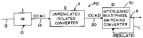
A first three stage power source PS 1 is shown in FIGURE I, including a first
stage I,
an unregulated isolated second stage II, and an interleaved multiphase third
stage converter
III. The first stage I in this embodiment includes an AC to DC converter 10
for converting
AC input signal 12 into a first DC output signal 14. The input 12 is a single
phase or a three
phase AC Iine supply with voltage that typically can vary between 115-575
volts, although
the invention is not limited to any particular number of input phases or to
any specific input
voltage values. Converter 10 is illustrated as an unregulated device which can
be in the form
of a rectifier and filter network to produce first DC output signal 14 (DC#1).
Since the AC
input signal is a line voltage, DC#1 is generally uniform in magnitude. In the
second stage
II, an unregulated inverter A is provided in the form of a DC to DC converter
with an
-13-
CA 02526523 2005-11-10
LEEE200536
isolation transfoxrner to convert the first DC output signal 14 (DC#1) into a
second DC
output signal 20 (DC#2).
The second DC output signal 20 forms the power input to stage III, which
includes a
multiphase interleaved DC to DC converter 30 for converting the second DC
output signal
S voltage on line 20 into a regulated signal (e.g., a current or voltage)
suitable for welding at
line B. A feedback control or regulation loop C senses a parameter in the
welding operation
for regulating the current, voltage, and/or power on output signal line B by
regulation of third
stage multiphase converter 30. In practice, converter 30 is a chopper or
switching converter,
such as a multiphase interleaved buck converter (e.g., FIGURES l0A-12B below),
although
use of a multiphase boost converter, buck-boost converter, cuk converter,
etc., or a
multiphase inverter are possible alternatives, wherein all such variant
implementations of a
multiphase converter axe contemplated as being within the scope of the
invention and the
appended claims. Further, the switching network of the second stage A can be
operated at a
frequency that is higher than the switching frequency of the third stage
converter 30 in the
three stage power source PSI as shown in FIGURE 1, although not a strict
requirement of
the invention. In addition, the second DC output signal voltage in line 20
(DC#2) can be
substantially less than the first DC output signal voltage from stage I on
line 14 (DC#1),
although not a requirement of the invention. In a preferred implementation,
moreover, an
isolation transformer can be provided in second stage inverter A, having an
input or primary
section or side with substantially more turns than a secondary section or side
used to create
the second DC output signal voltage DC#2 on Iine 20. In one particular
example, a
transformed turns ratio of 4:1 is used so that the second DC output signal
voltage on line 20
- I4-
CA 02526523 2005-11-10
LEEE200536
is about 1/4 the first DC output signal voltage DC#1 on line I4, although any
suitable turns
ratio can be used, where the first DC output signal voltage DC#I need not be
larger than the
second DC output signal voltage DC#2, and wherein the second stage II can be
unregulated.
FIGURE 2 illustrates another implementation of the invention wherein a three
stage
power source PS2 has essentially the same stage II and stage III as power
source PSI
described above. In the embodiment of FIGURE 2, however, input stage I is an
AC to DC
converter 40 including a rectifier followed by a regulated DC to DC converter
to provide the
first DC output signal DC#l . The converted signal is a DC output signal in
line 14 shown as
a first DC signal (DC#I). The first DC output signal voltage on line 14 is
regulated as
IO indicated by feedback line 42 in accordance with standard technology. Thus,
in one
implementation of power source PS2, first DC output signal DC#1 and second DC
output
signal DC#2 are controlled according to the regulation 42, and output welding
converter 30
is regulated by an output feedback loop C. With respect to first stage I,
first DC output
signal voltage DC#I on line 14 is regulated by feedback loop 42, wherein the
exemplary
1 S converter 40 also provides power factor correction by sensing the AC input
voltage
wavefonn 12 as represented by line 44. By using power source PS2 in FIGURE 2,
the first
DC output signal 14 is a fixed DC output signal voltage DC#I for different
single or three
phase voltages at input 12. Thus, second DC output signal voltage DC#2 at 20
is merely a
conversion of first DC output signal voltage DC#1 on line I4. Second DC output
signal
20 DC#2 in this implementation is thus a fixed voltage with a level determined
by the isolation
transformer and the fixed duty cycle of the switching network in unregulated
second stage
inverter A. This is a preferred implementation of the novel power source
employing three
-15-
CA 02526523 2005-11-10
LEEE200536
separate and distinct stages with stage II being an unregulated inverter for
converting a fixed
first DC output signal to a second fixed DC output signal used to drive a
regulated
interleaved multiphase switching converter 30, such as a chopper or inverter.
As another
possible alternative, stage I could be regulated by a feedback from DC #2 in
line 20, as
represented by a dashed feedback loop or line 46 in FIGURE 2.
Another possible implementation of a three stage power source PS3 is shown in
FIGURE 3 according to the invention, in which a first stage input converter 50
is regulated
by a feedback loop 52 from the welding current process output signal B, and
may further
control the first DC output signal DC#1 according to the first stage feedback
42 and
according to power factor correction via line 44. In the illustrated example
of FIGURE 3,
converter 50 is preferably regulated by the welding output feedback 52 and not
by the first
DC output signal voltage DC# 1 on line 14 as was the case in power source PS2
of FIGURE
2, although this feedback control architecture is not a requirement of the
present invention.
With regulation from welding output B in FIGURE 3, converter 50 is both a
power factor
correcting stage and a welding regulator. It is noted, however, that this
implementation of the
invention is disclosed for a complete technical disclosure of the three stage
power source as
contemplated by the present invention, and that power factor correction is not
a strict
Iilnitation of the invention.
As previously described, input stage I converts either a single phase or a
three phase
AC signal 12 into a fixed DC 14 (DC# 1 ) for use by the unregulated inverter A
constituting
second stage II. The implementation of the present invention generally employs
a DC to DC
converter 10, 40, 50 in stage I to produce the first DC output signal voltage
DC#1 at line 14
-16-
CA 02526523 2005-11-10
LEEE200536
in FIGURES 1-3. The DC to DC converter 10, 40, 50 of stage I can be selected
to create the
desired signal voltage DC# 1 on line 14, wherein an input rectifier provides a
DC voltage to a
first stage DC to DC converter (not shown) which may be a boost converter, a
buck
converter, a buck+boost converter, or other suitable DC to DC converter
architecture. Such a
DC to DC converter of the first stage I may advantageously perform power
factor correction
(e.g., FIGURES 2 and 3) by sensing the input AC waveform via line 44 and
controlling the
first DC output signal DC#1 in accordance therewith, in order to reduce
harmonic distortion
at the input 12 of the three stage power source PS2, PS3 and/or to ensure that
the input AC
current and voltage are in phase to the extent possible. The use of a power
factor correcting
input DC to DC converter 40, 50 is well known in the welding art and is used
in many prior
art two stage topographies, although power factor correction is not a strict
requirement for
practicing the present invention. In this regard, the puimary purpose of stage
I is to provide a
first DC (DC#1) at line 14 (indicated as lines 14a, 14b in subsequent
figures), which is then
used by the second stage II to produce a fixed DC (DC#2) in line 20 (indicated
by lines 20a,
20b in subsequent figures). It is noted that alternative implementations are
possible using a
non power factor correcting input or frst stage 10 as shown for example in
FIGURE 1,
wherein output lines of an input rectifier are coupled by a large storage
capacitor (not shown)
to produce a filtered, generally fixed, first DC output signal voltage DC#1 at
line 14. In
another alternative implementation, the first stage I could include a passive
power factor
correcting circuit 40, 50 connected to a single or multiphase AC input 12 to
produce a
generally fixed DC voltage at I4 (DC#1) as an input of the second stage
inverter A. The
above mentioned stage 1 architectures are merely examples and other input
stages could be
-17-
CA 02526523 2005-11-10
LEEE200S36
used in practicing the invention with either single phase or three phase input
signals, with or
without power factor correcting, and with or without regulation.
Referring also to FIGURE 4, in certain preferred implementations, a relatively
low
fixed second DC output signal DC#2 is provided on output 20 (e.g., illustrated
as lines 20a,
S 20b in FIGURES 4-10 and 12), wherein the multiphase third stage III of the
novel three stage
welding power source can be a chopper or other converter operated at a
frequency greater
than 18 kHz to provide the advantages of increased bandwidth. The switching
frequencies of
the unregulated second stage inverter A and the regulated output multiphase
converter 30
may, but need not, be different. In this regard, the switching frequency of
the multiphase
interleaved chopper output stage 30 can be substantially less than the
frequency of
unregulated inverter A in one example, although the specific frequency
relationship of the
second and third stages is not a strict requirement of the invention.
Power source PS4 shown in FIGURE 4 illustrates the use of the present
invention
wherein stage III includes an interleaved multiphase DC to DC switching
converter 30, and
I S further comprises a polarity switch 110 to facilitate AC welding 120 at
output terminals or
lines 1 10a and 1 10b, wherein the power source PS4 includes a third stage
controller 130
providing control signals 132 and 134 to converter 30 and to polarity switch
110,
respectively. The multiphase converter 30 is driven by a generally fixed input
DC 20 (first
DC output signal DC#1) and may be regulated by feedback from an AC or DC
welding
operation 120 to provide current suitable for welding across output leads 102,
104.
Moreover, the regulated signal may be provided through polarity switch 110 via
leads 1 10a
and 1 I Ob, as shown in FIGURE 4, in order to provide for AC welding, wherein
lead 102 is a
-18-
CA 02526523 2005-11-10
LEEE200536
positive polarity lead and lead 104 is a negative polarity lead. In this
regard, polarity switch
1 I 0 has a first position in which lead I02 is directed to the electrode of
the welding operation
I20 so the output of polarity switch 110 has a positive polarity on output
line 1 10a and a
negative polarity on output line I I Ob. This produces an electrode positive
(EP) DC welding
process at weld operation I20. Reversal of polarity switch network 1 IO can
produce an
electrode negative (EN) DC welding process at weld operation 120.
Thus, a DC welding process with either electrode negative or electrode
positive can
be performed according to the setting of the standard polarity switch I I 0.
In a like manner,
polarity switch 1 IO can be alternated between electrode negative and
electrode positive to
produce an AC welding process at weld operation 120. The polarity switch 1 I 0
thus drives
the DC output from regulated multiphase converter 30 to produce either an AC
welding
process or a DC welding process 120, which may advantageously be regulated and
controlled
via a feedback system indicated in FIGURE 4 as Line or loop 122 directed to
controller 130
for regulating multiphase converter 30 and for setting the polarity of switch
110 as indicated
by control signal lines 132, I 34, respectively. By thus regulating the
welding operation I20
at stage III, the unregulated inverter A at stage II can have a relatively
higher switching
frequency and high duty cycle to reduce the component sizes and to improve
efficiency
within the second stage II of the power source PS4.
Referring also to FIGURE 5, certain embodiments of the present invention
advantageously employ waveform control technology pioneered by The Lincoln
Electric
Company of Cleveland, Ohio, although not a strict requirement of the
invention. This type
of control system is schematically illustrated in FIGURE 5, wherein control
circuit 1 SO in the
-19-
CA 02526523 2005-11-10
LEEE200536
controller 130 of FIGURE 4 processes a waveform profile as a voltage on line
152a provided
by a wavefonn generator 152. The waveform profile is controlled by feedback
loop 122 as
schematically illustrated by error amplifier 154 having an output I 56. Thus,
the profile of
the waveform from generator 152 is controlled by the feedback loop 122 and
produces a
signal in output line 156. This line 156 is directed to an appropriate PWM
circuit 160
operated at a high frequency deternlined by the output of oscillator I62. This
frequency in
one example is greater than 18 kHz and is often higher than 40 kHz.
Furthermore, as
illustrated and described below with respect to FIGURES l0A-12B, the third
stage III
preferably provides out-of phase interleaved control of multiple third stage
converter power
circuits via the controller 130 using multiple phase adjusted PWM output
signals, and/or
using phase shifting or offset circuitry (not shown) to provide individual PWM
control
signals to the converter power circuits of the output stage III (e.g., FIGURE
I 1 below).
The output of the pulse width modulator 160, which may be implemented, for
example, in software and/or as a digital circuit within controller 130, is
shown as line 132 in
FIGURE 5 for controlling the waveform generated by multiphase switching third
stage
converter 30. The third stage converter output waveform (regulated signal
provided to
welding process 120) can have any profile and type, such as AC, DC, or
combinations
thereof, examples of which are schematically illustrated as waveforms
152b,152c, and 152d
at the right portion of FIGURE 5. In one AC welding example, waveform 152b is
provided
by the converter 30 in the form of an AC waveform of the type used in AC MIG
welding
where the negative electrode amperage is higher than the positive electrode
amperage.
Alternatively, the positive amperage may be higher than the negative amperage.
In
_20_
CA 02526523 2005-11-10
LEEE200536
waveforn 152c, the amperage for both electrode negative and electrode positive
is
essentially the same with the length of the negative electrode portion being
greater. Of
course, a process for AC welding can be adjusted to provide balanced AC
waveforms or
unbalanced AC waveforms, either in favor of electrode negative or electrode
positive, or the
balancing may change dynamically, where the time proportion and/or the
amplitude
proportion may be biased toward the negative electrode or positive electrode
side. When
polarity switch 110 is set for either a DC negative or a DC positive welding
operation (or
polarity switch 110 is omitted altogether, as in FIGURE 6 below), a pulse
welding
waveform, shown as waveform 1 SZd, is controlled by waveform generator 152 for
output of
a regulated signal from the converter 30 to the welding process 120. Various
other
waveforms, both AC and DC, can be controlled by controller 130 so the welding
operation
120 can be adjusted to be AC or DC. Furthermore, the welding operation can be
TIG, MIG,
submerged arc, or otherwise, wherein power source PS4 or other power sources
using the
present invention can be employed in performing any type of arc processing
operation. In
this regard, the process electrode (electrode E in FIGURES 7, 8, 10A, l OB,
and 12 below)
can be non-consumable or consumable, such as metal cored, flux cored, or solid
wire,
wherein a shielding gas may but need not be used according to the electrode
being employed.
All of these modifications in the welding operation can be performed in
systems employing
the various aspects of present invention.
Referring now to FIGURE 6, a modification of power source PS4 is illustrated
as
power source PSS to perforn DC welding. In this example, power source PSS
performs only
a DC welding operation 120 in which the feedback loop 122 is directed to
controller 130
-21 -
CA 02526523 2005-11-10
LEEE200536
having an output 132. Regulated converter 30 in the power source PS5 is
preferably a
multiphase chopper type switching DC to DC converter to produce a DC voltage
across lines
102a, 104a, wherein the controller 130 is preferably controlled by waveform
generator 152
(FIGURE 5). The polarity on lines I02a, 104a, moreover, can be electrode
negative or
electrode positive according to the demand of the DC welding process performed
at welding
operation 120. The regulated signal output by regulated converter 30,
furthermore, can be
more simplified than the welding output of power supply PS4 shown in FIGURE 4.
FIGURES 4 and 6, together with the control network or circuit 150 shown in
FIGURE 5,
illustrates the versatility of the novel three stage power source and the
interleaved multiphase
output converter 30 constituting the present invention, wherein the
illustrated embodiments
are merely examples and are not exhaustive of the possible implementations of
the present
invention.
Referring now to FIGURES 7 and 8; in implementing a two stage power source as
used in the prior art or a novel three stage power source of the present
invention, it is
necessary to provide a voltage for operating the controllers for both the
regulated and
unregulated switching networks used in these two types of power sources.
FIGURE 7
illustrates one preferred three stage architecture in accordance with the
present invention to
generate regulated signals for a welding operation and to provide control
voltages to operate
the various controllers of a three stage power source, such as power source
PS6. The use of
an output of a preregulator to provide the control voltage for the switching
controller of the
preregulator and switching controller of the second stage of a two stage power
source is well
known and is disclosed in Moriguchi 5,926,381, incorporated by reference
herein. Vdith
-22-
CA 02526523 2005-11-10
LEEE200536
respect to the final stage, an output chopper for performing a welding
operation routinely
obtains the controller control voltage from the input DC voltage to the
chopper. These two
well known technologies are incorporated in power source PS6.
The three stage power source PS6 in FIGURE 7 can be operated with controllers
having power supplies derived from various locations in the power source. In
particular,
power source PS6 has a first controller power supply 180 (PS#I) with an output
182 and
inputs 184, 186 from the first DC on leads 14a, 14b (DC#I). Power supply 180
includes a
buck convener or flyback converter, not shown, to reduce the high voltage DC#1
at the
output of preregulator 40 of FIGURE 2 to a low voltage on line I 82 suitable
for powering a
first stage controller 190. This control voltage on line 182 may be between 5
and 20 volts in
one example, although other voltages are possible within the scope of the
invention. Voltage
on Line I 82 is directed to first controller 190 having an output Iead 192 for
performing the
operation of preregulator 40 in accordance with standard technology. The
preregulator 40
may employ feedback from lines 42, 44 shown in FIGURES 2 and 3, and/or may
receive
welder output feedback along line 52, as indicated in FIGURE 3. Unregulated
second stage
inverter A in the exemplary implementations does not require a controller to
modulate the
duty cycle or the fixed relationship betv~Teen the input and output voltages,
but may receive a
control signal on an output lead I98 from a second controller I94 that
receives controller
operating voltage in line 196 from the first power supply 180.
As an alternative, a third power supply PS#3 is driven by one phase of input
12 to
give an optional power supply voltage 176 to first controller I90. Regulated
multiphase
switching converter 30 of stage III in this implementation has a second power
supply 200
23
CA 02526523 2005-11-10
LEEE200536
(PS#2) coupled to the second DC leads 20a and 20b via inputs 206 and 204,
respectively,
with a controller voltage on line 202 determined by the voltage on DC 20
(DC#2) illustrated
as including leads 20a, 20b. Power supply 200 includes a buck converter or
flyback
converter to convert the DC at the output of unregulated converter A to a
lower voltage for
use by third stage controller 130 having an output 132. The signal on line 132
regulates the
output of welding converter 30 in accordance with the feedback signal on line
C, as
discussed with respect to power sources PSI, PS2 in FIGURES 1 and 2,
respectively,
wherein the individual power circuits of multiphase converter 30 may be
independently
controlled by dedicated outputs 132 from controller 130, or a single PWM or
other type of
control output 132 may be temporally offset for individual power circuits of
the converter 30,
such that the individual third stage converter power circuits are operated out
of phase relative
to one another. DC 14 (DC#1 ) and DC 20 (DC#2) provide input to power supplies
180 and
200 respectively, which are DC to DC converters in one example for producing
low level DC
control voltage for controllers 190, 194 and/or 130. As an alternative shown
by dashed line
220 in FIGURE 7, first power supply 180 can also provide a control voltage for
the third
controller 130. FIGURE 7 has been disclosed to illustrate the versatility of
using a three
stage power source with controllers that can receive reduced supply voltages
from various
fixed DC voltage levels indicated to be PS#1 and PS#2. Other arrangements
could be
employed for providing the controller voltage, such as a rectified connection
to one phase of
AC input voltage 12 via lines 272 and 274 by a transformer in a manner
illustrated as PS#3.
Referring now to FIGURES 8 and 9, FIGURE 8 shows another implementation of the
present invention with more specific details on the preferred three stage
embodiment of the
-24-
CA 02526523 2005-11-10
LEEE200536
present invention, wherein a three stage power source PS7 is illustrated,
similar to power
source PS6 with Iike components having the same identification numbers. In
accordance
with an aspect of the invention, the output stage III includes a multiphase
interleaved
switching converter or chopper 30 for providing a regulated signal output
(e.g., a welding
current between electrode E and workpiece W). As shown in FIGURES 7 and 8, a
current
shunt S provides can be used to provide welding process current feedback
signal C to
controller 130. The illustrated high switching speed inverter A of stage II in
this
implementation includes the features and characteristics described above, and
additionally
provides electrical isolation between the first and second DC output signals
DC#1 and DC#2
I 0 via an isolation transformer 250 having a primary winding 252 and a
secondary winding 254.
As further illustrated in FIGURE 9, the puimary side of DC to DC converter A
includes a
switching network 300 for directing an alternating current to primary winding
252. The
rectified output from secondary 254 is the secondary section or side of
converter A.
The exemplary converter A of FIGURES 8 and 9 employs a high switching speed
inverter that has a duty cycle or phase shift set by the non-regulating
controller 194, wherein
no process or system feedback is provided to the controller 194 in the
illustrated
implementations. The second stage switching frequency, moreover, can be
relatively high
(e.g., higher than the switching speed of the third stage converter 30), such
as about 100 kHz
in the practical version of this power source PS7. In the exemplary
unregulated second stage
converter A, the duty cycle and operating frequency remain essentially fixed
during the
welding operation, although non-feedback type adjustments to the duty cycle
and/or
frequency of the second stage II can be made as indicated by "ADJ" circuit 260
having an
-25-
CA 02526523 2005-11-10
LEEE200536
output 262 for adjusting controller 194. In a preferred embodiment of the
second stage II,
moreover, the duty cycle thereof is close to 100% so that the switch pairs are
conductive
together their maximum times at the primary side of inverter A, although any
suitable
switching frequency and duty cycle may be employed within the scope of the
invention,
wherein circuit 260 or other means can be used to adjust the duty cycle, phase
shift,
frequency, etc. for the second stage II, in order to adjust the otherwise
generally fixed (e.g.,
unregulated) relationship between the first DC 14 and the second DC 20. Thus,
the
unregulated, isolation inverter A may be changed to have a different, but
fixed duty cycle. In
this regard, the duty cycle is preferably close to 100% so that the switch
pairs are operated
essentially in unison, wherein the duty cycle may be varied between about 80-
I00% in
typical applications of the present invention.
Input stage I normally includes a rectifier 60 followed by a power factor
correcting
DC to DC converter 62, wherein a suitable rectifier 60 can be provided for
single phase AC
or three phase AC signals of various magnitudes, represented as input 12. In a
preferred
implementation, moreover, the boost converter 62 is used for a power factor
correcting input
stage I to create the first DC output signal DC#1, as shown in FIGURE 8. This
boost
converter 62 is operated in accordance with controller 190 having a control
voltage 182 as
previously described. In accordance with a slight modification of the
preferred embodiment,
supply 270 in FIGURE 8 has a transformer connected by lines 272 and 274 across
one phase
of a single phase or three phase AC input 12. A rectifier and filter in power
supply 270
produce a low control voltage in optional dashed line 276 for use instead of
the control
voltage in line 182 if desired. These two alternatives do not affect the
operating
-26-
CA 02526523 2005-11-10
LEEE200536
characteristics of power source PS7. Other such modif canons of a three stage
power source
for electric arc welding can be obtained from the previous description and
well known
technology in the welding field.
Unregulated inverter A of stage II can use various inverter circuits, one of
which is
illustrated in greater detail in FIGURE 9. The preferred second stage circuit
A is divided
between a primary section or side defined by the input to primary winding 252
of isolating
transformer 250 and a secondary section or side defined by output of secondary
winding 254.
Referring first to the primary section or side of inverter A, full bridge
circuit 300 is
employed wherein paired switches SWI-SW3 and SW2-SW4 are across capacitor 348
are
connected by leads 302, 304, 306, and 308, although half bridge circuits or
other switching
circuits can alternatively be used. The switches SWI-SW4 in the illustrated
circuit 300 are
energized in alternate sequence by gating pulses. on lines 3I0, 312, 314, and
3I6,
respectively. Controller 194 outputs gating pulses in lines 310-3I6 and an
adjusted duty
cycle, frequency (period), and/or phase relationship may be determined by the
logic on Iine
262 from circuit 260 as previously discussed. In one implementation, the duty
cycle can be
controlled by changing the phase shift of lines 310 and 312 and lines 314 and
316, wherein
circuit 260 adjusts the duty cycle or phase shift of the paired switches. This
adjustment is
fixed during the operation of inverter A. In a preferred implementation,
circuit 300 has about
I00% duty cycle or phase shift, where each pair of switches has maximum
periods of
overlapping conduction. Controller 194 has a control voltage from an
appropriate supply
indicated in FIGURE 9 by line 196, as also previously described.
-27-
CA 02526523 2005-11-10
LEEE200536
In operation of the exemplary circuit 300 of FIGURE 9, an alternating current
is
directed through primary winding 252 by controlled operation of switches SW1-
SW4. This
current preferably has an ultra high frequency normally at least about 100 kHz
so the
components can be reduced in size, weight and cost, wherein such high
switching frequency
is not dictated by the welding operation, but is selected for efficiency of
unregulated stage A
of the three stage power source, although the specific frequency of operation
for the second
stage II is not a requirement of the present invention. The secondary section
or side of
inverter A includes a rectifier circuit 320 having rectifiers 322, 324, with
power inputs 330
and 332, outputs 342 and 340, and control inputs 326 and 328 gated by signals
on lines 326,
328, respectively, created at the opposite ends of secondary winding. Leads
326, 328, 330,
332, 340, and 342 form the output leads of rectifier 320 to create a DC
voltage (DC#2) across
leads 20a, 20b with the output current being smoothed by a choke 344 and the
resulting
output voltage being applied across an output filter capacitor 346.
In the exemplary three stage power source illustrated in FIGURES 8 and 9, the
second stage inverter A is unregulated, v~Thich means that it is not adjusted
by a real time
feedback signal from the welding operation or from the second DC output signal
DC#2.
Rather, the second stage II converts DC 14 (DC#1) to DC 20 (DC#2) in a
relatively fixed
manner without feedback regulation. In the illustrated second stage II, the DC
to DC
conversion provides a substantial reduction in the voltage directed to the
regulated third stage
30 of the power source using inverter A, through appropriate selection of the
transformer
turns ratio. In one example, the turns ratio of transformer 250 is about 4: l,
wherein the fixed
voltage on output 20 is about 1/4 the fixed voltage on output 14 of the first
stage, although
-28-
CA 02526523 2005-11-10
LEEE200536
any turns ratio can be used within the scope of the present invention. Several
advantages of
an unregulated stage are contained in an article entitled "The incredible
Shrinking
(Unregulated) Power Supply" by Dr. Ray Ridley incorporated by reference herein
as
background information. A basic advantage is the ability to increase the
frequency to above
100 kHz to reduce the size and cost of the second stage II.
Referring now to FIGURES 1 OA-12B, an aspect of the present invention involves
the
use of an interleaved multiphase switching converter 30 as the final (third)
stage of the three
stage welding power source. In this aspect of the invention, the third power
source stage III
comprises a plurality of converter power circuits to convert the second DC
output signal
DC#2 to a regulated signal suitable for a welding, cutting, or other arc
process, wherein the
various aspects of the third stage III are hereinafter exemplified in several
illustrative
embodiments of a four-phase buck type switching DC to DC converter 30 having
individual
converter power circuits 30a, 30b, 30c, and 30d coupled in parallel between
the second DC
output signal DC#2 and the welding operation to provide the process output
signal.
I S However, it will be appreciated that any number N converter power circuits
may be
employed in a multiphase third stage converter within the scope of the
invention, wherein N
can be any positive integer greater than 1. In addition, any converter power
circuit type may
be used, wherein the invention is not limited to buck converter power circuit
architectures.
Moreover, the exemplary third stage converter power circuits 30a-30d are
operated out of
phase relative to one another as shown in FIGURE 11 below, although this
particular form of
converter power circuit control illustrated herein is not a strict requirement
of the invention.
-29-
CA 02526523 2005-11-10
LEEE200536
FIGURE 10A illustrates an implementation of the multiphase interleaved third
stage
converter 30 configured in a high side buck type architecture in which the
individual
switching elements and output chokes of the converter power circuits 30a-30d
are coupled
between the positive second DC output signal line 20a and the welding
electrode E (process
output B) with a current shunt feedback sensor S in the negative (workpiece)
return path. An
alternative four-phase buck converter implementation is shown in FIGURE l OB,
wherein the
converter phase switches and inductor chokes are in a negative return path
between the
workpiece W and the negative second DC output signal line 20b. In each of
these examples,
the converter power circuits 30a-30d individually comprise a switching device
Q, such as
bipolar transistor (e.g., IGBT, etc.), MOSFET, or other switching element,
along with a
rectifier D and an inductor or choke L, wherein these components are arranged
in a buck type
converter power circuit configuration. Alternatively, the converter power
circuit components
may be configured differently, for example, to achieve boost, buck-boost, or
other converter
type architectures, and the converter power circuits may alternatively
comprise more or
fewer components than the exemplary buck converter power circuits of the
illustrated
embodiments, wherein all such variant implementations which provide multiphase
DC to DC
conversion to provide a regulated signal suitable for an arc process in a
third stage of a
welding power source are contemplated as falling within the scope of the
invention and the
appended claims.
As shown in FIGURE 10A, one possible multiphase converter 30 comprises four
such buck converter power circuits 30a-30d. The fzrst converter power circuit
30a includes a
switching device Q1 coupled between the positive Iine 20a of the second DC
output signal
-30-
CA 02526523 2005-11-10
LEEE200536
DC#2 and an internal buck converter power circuit node, wherein Q I is a
bipolar transistor
having a collector coupled to line 20a, an emitter coupled with the converter
power circuit
internal node, and a control terminal (base or gate) coupled to receive a
first converter power
circuit control signal 132a (~A) from the controller 130. The first buck
converter power
circuit 30a further comprises a rectifier (freewheeling diode) D 1 having an
anode coupled to
the negative line 20b of the second DC output signal DC#2 and a cathode
coupled to the
emitter of QI (the internal node), as well as a converter power circuit
inductor Ll coupled
between the internal node and the regulated signal. The other three buck
converter power
circuits 30b-30d are similarly constructed, with corresponding switching
devices Q2-Q4,
diodes D2-D4, and inductors L2-L4, respectively. As shown in FIGURE 10A, the
converter
power circuit switching devices Ql-Q4 are all coupled between the input
terminal 20a and
the corresponding internal power circuit nodes, and the inductors L 1-L4 are
all coupled to the
welding electrode is the regulated signal line B, where the controller 130
provides
corresponding power circuit control signals ~A-d~D to the switches Q 1-Q4 of
the converter
power circuits 30a-30d.
Referring also to FIGURE 11, the third stage controller I30 provides the
control
signals I 32a-132d such that the individual converter power circuits 30a-30d
are pulse width
modulated according to feedback signal C from the current shunt S, and each
converter
power circuit 30a-30d is active for a corresponding active portion having
duration of a
switching period T of the multiphase converter 30. Moreover, the converter
power circuits
30a-30d are controlled in interleaved fashion, wherein the controller 130
provides the
switching control signals I32a-132d such that the buck converter power
circuits 30a-30d are
31 _
CA 02526523 2005-11-10
LEEE200536
operated out of phase relative to one another. Any phase relationship is
contemplated within
the scope of the invention, including 0 degrees (e.g., in-phase), wherein the
exemplary
implementations illustrated and described herein provide for a relative phase
angle that is
related to the number N of conveuter power circuits 30a-30d (e.g., four in the
illustrated
examples). Moreover, the converter power circuits in one aspect of the
invention are
operated such that at least two are concurrently operating during at least a
portion of each
switching cycle, whereby some or all of the circuits operated with temporal
overlap for
certain values of pulse width. In this regard, the illustrated example of
FIGURE 11 shows 90
degree phase angle between the successive converter power circuits, with the
switching
periods overlapping one another.
A timing or waveform diagram 3 I in FIGURE 11 illustrates exemplary power
circuit
switching control signals 132a-132d (indicated as transistor control voltages
~A-~D for tzvo
exemplary switching periods of the interleaved four-phase converter 30,
wherein each
converter switching period has a time duration T and the individual power
circuits are active
(e.g., pulse width modulated) in corresponding portions also of duration T,
wherein the
active portions are phase shifted by an angle that is 360 degrees/N. FIGURE 11
also
illustrates the corresponding converter power circuit switching device
currents IQ,- IQ,. In the
exemplary four-phase converters 30 illustrated and described herein, each
switching cycle or
period T of the converter 30 includes 360 degrees, wherein the active portion
T for each
converter power circuit 30a-30d begins at a multiple of the 90 degree phase
angle. Other
relative phase relationships are possible within the scope of the invention,
including in-phase
operation. In general, the interleaved multiphase converters of the invention
may include any
-32-
CA 02526523 2005-11-10
LEEE200536
number N converter power circuits, where N is an integer greater than l, and
wherein the
phase angles may vary from 0 to 360 degrees.
As shown in the timing diagram 31 of FIGURE I l, the individual buck converter
power circuits operate in normal buck converter fashion, with the controller
130 providing
the control signals I32a-I32d in interleaved phase-shifted fashion to generate
the regulated
process output signal to the welding electrode E on line B. With respect to
the first converter
power circuit 30a, for example, when the first converter power circuit switch
QI is
conducting (Q1 turned ON by control signal 132a (~A), with a positive switch
current IQ,
flowing through switch Q 1 ), the internal node rises to the voltage at line
20a, and the current
through inductor L 1 ramps up in a generally linear fashion to provide welding
current to the
electrode E via line B. When QI is turned off, the switch current IQ, ceases,
the inductor
current continues to flow, wherein the internal node voltage drops and the
freewheeling
diode D 1 becomes forward biased and begins to conduct. In the four-phase
example, the
pulse width modulation of the first converter power circuit 30a begins at zero
degrees of each
designated switching period T, wherein the controller I30 provides the first
control signal
132a (~A) having a given on time ToNA, wherein the ratio of the on time ToN"
to the
switching period T corresponds to a PWM duty cycle determined by the
controller 130 based
on comparison of the sensed welding process current and a desired welding
current (e.g.,
according to waveform control as shown in FIGURE 5 above), or according to any
other
suitable control strategy employing feedback, feed forward, or other algorithm
or control
scheme. The other converter power circuits 30b-30d axe similarly controlled by
signals
I 32b-1 32d from controller 130 in this example, with the respective on-times
To~,~ Toy being
-33-
CA 02526523 2005-11-10
LEEE200536
also determined according to the feedback and waveform control strategy, and
with the
active portions beginning in successively phase-shifted fashion, with the
period T for the
second circuit 30b starting at 90 degrees, and that of circuits 30c and 30d
starting at 180 and
270 degrees, respectively. In this manner, each converter power circuit
contributes current to
the welding operation during the corresponding portion of each welding period
T, wherein
the currents thereof are additive at the output. It is noted in this regard,
that the output
voltage is essentially unrelated to the number N of converter power circuits.
In other
possible implementations, the active time portions of each power circuit need
not be equal,
and the power circuits need not be controlled according to the same strategy.
Moreover,
although the exemplary controller 130 employs pulse width modulation
techniques, other
modulation can be employed, such as pulse frequency modulation, etc., wherein
all such
alternative implementations are contemplated as falling within the scope of
the invention and
the appended claims.
Referring also to FIGURE IOB, an alternative four-phase buck-type interleaved
converter 30 is illustrated, in which the converter power circuits 30a-30d
individually
comprise a switching device Ql-Q4 coupled between the second DC output signal
and an
internal power circuit node. The switching devices Ql-Q4 are coupled to the
negative line
20b of the second DC output signal DC#2 in the configuration of FIGURE 10B,
and the
power circuit inductors L 1-L4 are coupled between the corresponding buck
converter power
circuit internal nodes and the regulated signal at the workpiece W, wherein a
current shunt S
is provided in the positive path at line B to generate the feedback on line C.
In this
embodiment, the freewheeling diodes Dl-D4 of the convei°ter power
circuits 30a-30d are
_34_
CA 02526523 2005-11-10
LEEE200536
coupled with an anode at the power circuit internal nodes and a cathode
coupled to the
positive DC line 20a. In this case, the control signals 132a-132d axe provided
as shown in
the tuning diagram 31 of FIGURE 11 as in the above described example for
interleaved
pulse width modulation of the converter power circuits 30a-30d. When Q 1 is on
(e.g., ToNA),
the first power circuit internal node is at the voltage of line 20b and
current IQl flows from
the first inductor LI to the negative DC line 20b. As the switch Q 1 is turned
off, the inductor
current continues to flow through the freewheeling diode D 1 to the line 20a
and hence to the
welding process electrode E. As discussed above, other particular power
circuit types and
designs may be substituted for the exemplary buck converter power circuits 30
of FIGURES
10-A and 1 OB within the scope of the invention.
It is noted that the use of multiple power circuits 30a-30d in the switching
converter
30 of the third stage III provides several advantages over non-multiphase
approaches. One
particular advantage is reduced ripple current. In this regard, the converter
power circuits
30a-30d are similarly constructed, each of which having a converter power
circuit ripple
current rating Ipr, wherein the interleaved multiphase switching converter 30
has a conveuter
ripple current rating Icr which is less than the rating Ipr of the individual
power circuits.
This reduction in the ripple current results from the multiphase architecture,
and allows
reduction in the size and values of the converter power circuit inductors Ll-
L4, thereby
saving space and cost. This reduction, for example, may offset the increased
component
count necessitated by the multiphase design. Furthermore, the reduced inductor
size may
facilitate the use of board mounted chokes instead of larger chokes found in
single phase
converters. Moreover, the reduced values of the inductors can improve the
transient response
-35-
CA 02526523 2005-11-10
LEEE200536
of the output stage III, thereby facilitating advanced welding process control
strategies (e.g.,
waveform control, etc.).
In addition, the individual power circuits 30a-30d can be designed for a given
maximum current rating with the number of power circuits in a given power
source design
being determined by the desired converter current output, whereby different
welding or
plasma cutting systems can be designed using different numbers of modular
chopper power
circuits. Furthermore, since the currents provided by the individual power
circuits are
relatively low, high efficiency and low current stresses can be achieved,
while providing
potentially unlimited bandwidth for advanced welding techniques. Unlike prior
attempts at
multiphase welding power sources, such as Reynolds 6,051,804 and 6,300,589,
the three
stage welding power sources of the present invention are operable at virtually
any current
amperage where the individual converter power circuit modules can be designed
for
operation at typical welding voltage levels, where the welder output voltage
is essentially
unrelated to the number N of output stage converter power circuits. In this
regard, the
interleaved multiphase switching converters (e.g., converter 30) of the
invention comprises N
converter power circuits (e.g., power circuits 30a-30d) coupled in parallel to
receive the
second DC output signal (DC#2) where the power circuits individually have a
converter
power circuit maximum current rating Ip, and wherein the interleaved
multiphase switching
converter has a converter maximum current rating of about N x Ip. For example,
if buck
converter power circuit 30a is designed for operation at a maximum power
circuit current Ip
of 50 amperes, a 300 ampere multiphase converter could be constructed using
six such
converter power circuits coupled in parallel to convert power from the second
DC output
-36-
CA 02526523 2005-11-10
LEEE200536
signal DC#2 to a welding regulated signal, wherein each converter power
circuit could be
operated at a 60 degree relative phase relationship for a switching period
duration T.
Referring now to FIGURES I 2-12B, another aspect of the invention provides a
three
stage power source with a first stage converting an input AC signal to provide
a first DC
output, a second stage to convert the first DC output signal into a second DC
output signal,
and an interleaved multiphase tMrd stage for converting the second DC output
signal to a
regulated signal, wherein the multiphase converter comprises a plurality of
converter power
circuits individually having an inductor and a switching device, wherein at
least two of the
inductors are wound on a common core. FIGURE I2 illustrates the exemplary
multiphase
IO buck converter 30 having four converter power circuits 30a-30d, where the
power circuit
components are interconnected in a buck type converter arrangement similar and
electrically
equivalent to that illustrated in FIGURE I OA above. In the implementation of
FIGURE 12,
however, the power circuit inductors L 1-L4 are integrated with one another
using a common
core, to form an integrated magnetic component or unitary converter inductor
structure 30L.
Other embodiments of this aspect of the invention are possible wherein less
than all of the
inductors axe combined on a single core. The inductors Ll-L4 each include a
corresponding
winding, where two or more of the windings of the inductors L I -L4 may be
wound ar ound a
common core, which may be any suitable form or material, such as E-I, E-E or
other core
structures as are known. The integration of two or more of the converter power
circuit
inductors LI-L4 may allow for further system size and cost reduction in the
three stage
power source architectures of the invention.
-37-
CA 02526523 2005-11-10
LEEE200536
In constructing an integrated converter structure in the multiphase output
stage of the
invention, the relative orientations of the inductor windings may be aligned
as shown in
FIGURE 12A, or may be alternated or staggered as shown in an alternate
embodiment 30La
in FIGURE 12B. In this regard, the selection of a particular core design and
the relative
winding orientation in a given design can be varied to selectively provide for
alternate or
inverse couplings, wherein the individual power circuit inductors thus
integrated may be
coupled or decoupled, as taught in ~umel "Magnetic Integration fox Interleaved
Converters".
Integration of decoupled inductors L1-L4 itself may advantageously provide
reduction in
total component size, as well as lowered losses and cost. Magnetic coupling of
some or all
of the inductors LI-L4 allows energy from one inductor to be transferred to
another coupled
inductor, wherein output filtering requirements may be reduced. Thus, for
example, a
decoupled alternate integration could be provided with staggered windings in
the integrated
magnetic component 30La (FIGURE 12B), in which the common core may be
constructed
with the integrated windings being wound around parallel gapped magnetic core
legs,
wherein one or more additional ungapped legs are provided to magnetically
decouple the
inductors from one another. In another possible implementation (FIGURE 12A),
the
windings of the integrated inductors L I -L4 are wound around gapped or
ungapped legs of a
core structure without additional decoupling legs, whereby the integrated
inductors are
magnetically coupled. Thus, whereas the multiphase output stage conversion
aspects of the
invention can facilitate the above mentioned advantages of improved dynamic
response and
higher bandwidths generally, selective integration of two or more converter
power circuit
-38-
CA 02526523 2005-11-10
LEEE200536
inductors may provide further benefits, particularly where a relatively large
number of
converter power circuits are used (e.,g., high values of N).
While the invention has been illustrated and described with respect to one or
more
exemplary implementations or embodiments, equivalent alterations and
modifications will
occur to others skilled in the art upon reading and understanding this
specification and the
annexed drawings. In particular regard to the various functions performed by
the above
described components (assemblies, devices, systems, circuits, and the like),
the terms
(including a reference to a "means") used to describe such components are
intended to
correspond, unless otherwise indicated, to any component which performs the
specified
I O function of the described component (i.e., that is functionally
equivalent), even though not
structurally equivalent to the disclosed structure which performs the function
in the herein
illustrated exemplary implementations of the invention. In addition, although
a particular
feature of the invention may have been disclosed with respect to only one of
several
implementations, such feature may be combined with one or more other features
of the other
implementations as may be desired and advantageous for any given or particular
application.
Also, to the extent that the terms "including", "includes", "having°',
"has", "with", or variants
thereof axe used in the detailed description and/or in the claims, such terns
are intended to be
inclusive in a manner similar to the term "comprising."
-39-