Language selection

Search

Patent 2527146 Summary

Third-party information liability

Some of the information on this Web page has been provided by external sources. The Government of Canada is not responsible for the accuracy, reliability or currency of the information supplied by external sources. Users wishing to rely upon this information should consult directly with the source of the information. Content provided by external sources is not subject to official languages, privacy and accessibility requirements.

Claims and Abstract availability

Any discrepancies in the text and image of the Claims and Abstract are due to differing posting times. Text of the Claims and Abstract are posted:

  • At the time the application is open to public inspection;
  • At the time of issue of the patent (grant).
(12) Patent Application: (11) CA 2527146
(54) English Title: MULTI-MODE RADIO WITH INTERFERENCE CANCELLATION CIRCUIT
(54) French Title: RADIO MULTIMODE PRESENTANT UN CIRCUIT D'ANNULATION D'INTERFERENCE
Status: Deemed Abandoned and Beyond the Period of Reinstatement - Pending Response to Notice of Disregarded Communication
Bibliographic Data
(51) International Patent Classification (IPC):
  • H04B 01/40 (2015.01)
  • H04B 01/10 (2006.01)
  • H04B 01/48 (2006.01)
  • H04W 88/06 (2009.01)
(72) Inventors :
  • AXNESS, TIMOTHY A. (United States of America)
  • KAZAKEVICH, LEONID (United States of America)
(73) Owners :
  • INTERDIGITAL TECHNOLOGY CORPORATION
(71) Applicants :
  • INTERDIGITAL TECHNOLOGY CORPORATION (United States of America)
(74) Agent: SMART & BIGGAR LP
(74) Associate agent:
(45) Issued:
(86) PCT Filing Date: 2004-05-21
(87) Open to Public Inspection: 2004-12-29
Examination requested: 2005-11-24
Availability of licence: N/A
Dedicated to the Public: N/A
(25) Language of filing: English

Patent Cooperation Treaty (PCT): Yes
(86) PCT Filing Number: PCT/US2004/016164
(87) International Publication Number: US2004016164
(85) National Entry: 2005-11-24

(30) Application Priority Data:
Application No. Country/Territory Date
60/473,600 (United States of America) 2003-05-27

Abstracts

English Abstract


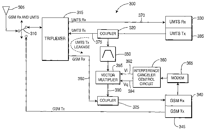
A multi-mode wireless transmit/receive unit (WTRU) includes at least one
antenna, first and second communication mode receivers and a first
communication mode transmitter. The first and second receivers simultaneously
receive signals from the antenna. The first transmitter generates and sends a
first type of signal to the antenna while, at the same time, the second
receiver receives a second type of signal from the antenna. In a preferred
embodiment, the WTRU further includes a vector multiplier configured to reduce
or eliminate interference of signals received by the second receiver, the
interference being caused by the first transmitter. The vector multiplier
adjusts the phase and amplitude of noise (i.e., spurious in-band noise)
measured by the second receiver. The WTRU may further include a second
communication mode transmitter configured to generate and send a second type
of signal to the antenna.


French Abstract

L'invention concerne une unité de transmission/réception sans fil (WTRU) multimode comprenant au moins une antenne, un premier récepteur de mode de communication et un second récepteur de mode de communication, et un premier émetteur de mode de communication. Le premier récepteur et le second récepteur reçoivent simultanément des signaux provenant de l'antenne. Le premier émetteur génère et envoie un premier type de signal à l'antenne, tandis que, au même moment, le second récepteur reçoit un second type de signal provenant de l'antenne. Dans un mode de réalisation préféré, le WTRU comprend également un multiplicateur de lecteur configuré pour réduire ou pour éliminer une interférence de signaux reçus par le second récepteur. Cette interférence est provoquée par le premier émetteur. Le multiplicateur de vecteur règle la phase et l'amplitude du bruit (notamment, bruit parasite de la bande) mesurées par le second récepteur. Le WTRU peut également comprendre un second émetteur de mode de communication configuré pour générer et pour envoyer un second type de signal à l'antenne.

Claims

Note: Claims are shown in the official language in which they were submitted.


CLAIMS
What is claimed is:
1. A multi-mode wireless transmit/receive unit (WTRU) comprising:
(a) at least one antenna configured to receive and transmit at
least two different types of signals;
(b) a first communication mode receiver configured to receive
a first type of signal from the antenna;
(c) a second communication mode receiver configured to
receiving a second type of signal from the antenna; and
(d) a first communication mode transmitter configured to
generate and send the first type of signal to the antenna, wherein the first
and
second communication mode receivers simultaneously receive signals from the
antenna, and the first transmitter sends the first type of signal to the
antenna
while, at the same time, the second receiver receives the second type of
signal
from the antenna.
2. The WTRU of claim 1 further comprising:
(e) a vector multiplier configured to reduce or eliminate
interference of signals received by the second communication mode receiver,
the
interference being caused by the first communication mode transmitter, wherein
the vector multiplier adjusts the phase and amplitude of the interference.
3. The WTRU of claim 1 further comprising:
(e) a second communication mode transmitter configured to
generate and send the second type of signal to the antenna; and
(f) a switch in communication with the antenna, the switch
being configured to selectively connect the second communication mode
transmitter to the antenna, prevent signals from the antenna to reach the
first
and second communication mode receivers, and prevent the first communication
mode transmitter from sending the first type of signal to the antenna.
-7-

4. The WTRU of claim 1 wherein the first communication mode
receiver is a universal mobile telecommunications system (UMTS) receiver.
5. The WTRU of claim 1 wherein the second communication mode
receiver is a global system for mobile communications (GSM) receiver.
6. The WTRU of claim 1 wherein the first type of signal is a frequency
division duplex (FDD) signal.
7. The WTRU of claim 6 wherein the first type of signal received by the
first communication mode receiver is originated by a universal terrestrial
radio
access (UTRA) - FDD cell.
8. The WTRU of claim 1 wherein the second type of signal is a time
division multiple access (TDMA) signal.
9. The WTRU of claim 8 wherein the second type of signal received by
the second communication mode receiver is originated by a universal
terrestrial
radio access (UTRA) - TDD cell.
10. The WTRU of claim 8 wherein the second type of signal received by
the second communication mode receiver is originated by a global system for
mobile communications (GSM) cell.
11. An integrated circuit (IC) used in combination with at least one
antenna configured to receive and transmit at least two different types of
signals,
the IC comprising:
(a) a first communication mode receiver configured to receive
a first type of signal from the antenna;
(b) a second communication mode receiver configured to
receive a second type of signal from the antenna; and
-8-

(c) a first communication mode transmitter configured to
generate and send the first type of signal to the antenna, wherein the first
and
second communication mode receivers simultaneously receive signals from the
antenna, and the first transmitter sends the first type of signal to the
antenna
while, at the same time, the second receiver receives the second type of
signal
from the antenna.
12. The IC of claim 11 further comprising:
(d) a vector multiplier configured to reduce or eliminate
interference of signals received by the second communication mode receiver,
the
interference being caused by the first communication mode transmitter, wherein
the vector multiplier adjusts the phase and amplitude of the interference.
13. The IC of claim 11 further comprising:
(d) a second communication mode transmitter configured to
generate and send the second type of signal to the antenna; and
(e) a switch in communication with the antenna, the switch
being configured to selectively connect the second communication mode
transmitter to the antenna, prevent signals from the antenna to reach the
first
and second communication mode receivers, and prevent the first communication
mode transmitter from sending the first type of signal to the antenna.
14. The IC of claim 11 wherein the first communication mode receiver is
a universal mobile telecommunications system (UMTS) receiver.
15. The IC of claim 11 wherein the second communication mode receiver
is a global system for mobile communications (GSM) receiver.
16. The IC of claim 11 wherein the first type of signal is a frequency
division duplex (FDD) signal.
-9-

17. The IC of claim 16 wherein the first type of signal received by the
first communication mode receiver is originated by a universal terrestrial
radio
access (UTRA) - FDD cell.
8. The IC of claim 11 wherein the second type of signal is a time
division multiple access (TDMA) signal.
19. The IC of claim 18 wherein the second type of signal received by the
second communication mode receiver is originated by a universal terrestrial
radio
access (UTRA) - TDD cell.
20. The IC of claim 18 wherein the second type of signal received by the
second communication mode receiver is originated by a global system for mobile
communications (GSM) cell.
-10-

Description

Note: Descriptions are shown in the official language in which they were submitted.


CA 02527146 2005-11-24
WO 2004/114683 PCT/US2004/016164
[0001] MULTI-MODE RADIO WITH INTERFERENCE
CANCELLATION CIRCUIT
[0002] FIELD OF THE INVENTION
[0003] The present invention relates generally to wireless communication
systems. More particularly, the present invention relates to attenuating
spurious transmissions which interfere with communications received by a
receiver in a wireless communication system.
[0004] BACKGROUND
[0005] In a conventional cellular communication system including a
plurality of wireless transmit/receive units (WTRUs), (i.e., user equipments
(UEs), radios, mobile platforms, handsets), and a network, the WTRUs are
required to measure signals from different cells in order to find base
stations
with the strongest signal and report them to the network for facilitating
handover (connected mode) and cell reselection (idle mode). When a new base
station with a stronger signal than a current serving base station is
measured,
the network will instruct the respective WTRU to handover to the new base
station. These measurements are typically performed on common channels, such
as the pilot channel in Code Division Multiple Access (CDMA) networks and the
Broadcast Control Channel (BCCH) in Global System for Mobile communications
(GSM) networks.
[0006] Multi-mode WTRUs support more than one Radio Access Technology
(RAT). For example, a multi-mode WTRU may include support for Universal
Terrestrial Radio - Frequency Division Duplex (UTRA-FDD) CDMA and GSM.
Usually, multi-mode WTRUs are required to support handover between different
RATS. Such handovers are referred to as inter-RAT handovers.
[0007] A problem arises for the case of multi-mode WTRUs in which one of
the modes requires constant transmissions. For example, during an active
UTRA-FDD CDMA call, i.e., when in "connected mode", the WTRUs continuously
transmit and receive in different frequency bands. In order to make a
-1-

CA 02527146 2005-11-24
WO 2004/114683 PCT/US2004/016164
measurement for an inter-RAT handover, such as to a GSM or Time Division
Synchronous Code Division Multiple Access (TD-SCDMA) network, the WTRU
must stop transmitting during the measurement period. Otherwise, emissions
from the CDMA transmitter will interfere with the receiver belonging to the
other RAT.
[0008] Figure 1 illustrates the interference problem described above. A
frequency spectrum 100 includes a UTRA-FDD signal in the 1920 - 1980 MHz
band 105 having spurious emissions 110 that fall within the GSM Digital
Cellular System (DCS) 1800 receive band 115 from 1805 - 1880 MHz. The
UTRA-FDD signal 105 itself acts as a large out-of band blocker for the GSM
receiver and desensitizes the receiver if not attenuated. Known practical
filter
solutions provide some attenuation of the UTRA-FDD signal, but the small
frequency spacing and cost/size constraints results in inadequate filtering
which
does not affect the level of the spurious transmission from the UTRA-FDD
transmitter.
[0009] Networks that require continuous transmissions using multi-mode
operation avoid this problem by allowing the WTRU to create gaps in its
transmissions. During the gap period, the WTRU stops transmitting to the
serving cell. Instead, the WTRU receives signals from neighboring cells
belonging to a different system. For example, by implementing a compressed
mode in UTRA-FDD, the WTRU is able to take advantage of the gaps in
transmissions to make measurements on GSM cells.
[0010] Figure 2 illustrates an example of a conventional WTRU 200 which
implements a compressed mode operation. The WTRU 200 includes an antenna
205, a system switch 210, a duplexer 215, a universal mobile
telecommunications
system (UMTS) receiver (Rx) 220, a UMTS transmitter (Tx) 225, a
transmitlreceive switch 230, a bandpass filter 235, a GSM Rx 240, and a GSM Tx
245. The system switch 210 is used to selectively connect the antenna 205 to
one
of a UMTS (e.g., UTRA-FDD) radio or a GSM radio. By implementing the
compressed mode, cell capacity is reduced because communications which occur
between the WTRU 200 and the network is interrupted during the above-
-2-

CA 02527146 2005-11-24
WO 2004/114683 PCT/US2004/016164
mentioned transmission gaps. A multi-mode radio that simultaneously receives
i
signals from a UTRA-FDD cell and a Time Division Multiple Access (TDMA) cell
to avoid such an interruption in communications is desired. Furthermore, a
multi-mode radio that allows the GSM Rx 240 to receive signals without
interference from the UMTS Tx 225 is also desired.
[0011] SUMMARY
[0012] A multi-mode WTRU includes at least one antenna, a first
communication mode receiver, a second communication mode receiver and a first
communication mode transmitter. The antenna is configured to receive and
transmit at least two different types of signals. The first communication mode
receiver is configured to receive a first type of signal from the antenna. The
second communication mode receiver is configured to receive a second type of
signal from the antenna. The first communication mode transmitter is
configured to generate and send the first type of signal to the antenna. The
first
and second communication mode receivers simultaneously receive signals from
the antenna. The first transmitter sends the first type of signal to the
antenna
while, at the same time, the second receiver receives the second type of
signal
from the antenna.
[0013] The WTRU may further include a vector multiplier configured to
reduce or eliminate interference of signals received by the second
communication
mode receiver, the interference being caused by the first communication mode
transmitter. The vector multiplier adjusts the phase and amplitude of the
interference.
[0014] The WTRU may further include a second communication mode
transmitter configured to generate and send the second type of signal to the
antenna, and a switch in communication with the antenna. The switch may be
configured to selectively connect the second communication mode transmitter to
the antenna, prevent signals from the antenna to reach the first and second
communication mode receivers, and prevent the first communication mode
transmitter from sending the first type of signal to the antenna.
-3-

CA 02527146 2005-11-24
WO 2004/114683 PCT/US2004/016164
[0015] The first communication mode receiver may be a universal mobile
telecommunications system (UMTS) receiver. The second communication mode
receiver may be a global system for mobile communications (GSM) receiver. The
first type of signal may be a frequency division duplex (FDD) signal. The
first
type of signal received by the first communication mode receiver may be
originated by a universal terrestrial radio access (UTRA) - FDD cell. The
second
type of signal may be a TDMA - FDD signal. The second type of signal received
by the second communication mode receiver may be originated by a universal
terrestrial radio access (UTRA) - TDD cell. The second type of signal received
by
the second communication mode receiver may be originated by a global system
for mobile communications (GSM) cell.
[0016] BRIEF DESCRIPTION OF THE DRAWINGS
[0017] A more detailed understanding of the invention may be had from the
following description of a preferred example, given by way of example and to
be
understood in conjunction with the accompanying drawing wherein:
[0018] Figure 1 provides an example of interference in a multi-mode
WTRU;
[0019] Figure 2 shows an example of a conventional multi-mode WTRU
requiring compressed mode for performing measurements; and
[0020] Figure 3 provides a system block diagram of a WTRU
incorporating an interference cancellation circuit in accordance with a
preferred embodiment of the present invention.
[0021] DETAILED DESCRIPTION OF THE PREFERRED EMBODIMENTS
[0022] The following is a description of a preferred embodiment of a WTRU
or integrated circuit (IC) used to communicate with a UTRA-FDD cell of a
wireless multi-cell FDD communication system while receiving signals from a
TDMA cell, such as a GSM or UTRA-TDD Bell. When the WTRU is not in a
connected mode, the WTRU must periodically search for new base stations.
Typically the WTRU must do this as efficiently as possible to minimize power
-4-

CA 02527146 2005-11-24
WO 2004/114683 PCT/US2004/016164
consumption, thus maximizing battery life. This can be performed most
efficiently if the WTRU can simultaneously receive signals from an FDD cell
and
a TDMA cell.
[0023] Preferably, the present invention disclosed herein is incorporated
into a wireless transmit/receive unit (WTRU). Hereafter, a WTRU includes but
is not limited to a user equipment, mobile station, fixed or mobile subscriber
unit,
pager, or any other type of device capable of operating in a wireless
environment.
The features of the present invention may be incorporated into an IC or be
configured in a circuit comprising a multitude of interconnecting components.
[0024] The present invention is applicable to communication systems using
TDD, TDMA, FDD, CDMA, CDMA 2000, time division synchs onous CDMA
(TDSCDMA), and orthogonal frequency division multiplexing (OFDM). However,
the present invention is envisaged to be applicable to other types of
communication systems as well.
[0025] Figure 3~is a block diagram showing a preferred embodiment of a
interference cancellation system which is incorporated into a WTRU 300. The
WTRU includes an antenna 305, a transmit/receive switch 310, a triplexes 315,
first coupler 320, second coupler 325, a UMTS Rx 330, a UMTS Tx 335, a GSM
Rx 340, a GSM Tx 345, a bandpass filter 350, an in-phase/quadrature (I/Q)
vector
multiplier 355, a interference canceler control circuit 360 and a modem 365.
When the WTRU 300 is in a receive mode, signal arriving at the antenna 305 are
forwarded to the transmit/receive switch 310. The transmit/receive switch 310
connects the antenna to the triplexes 315 for UMTS and GSM Rx operation.
When the WTRU 300 is in a GSM Tx mode, the transmit/receive switch 310
connects the antenna to the GSM Tx 345 during GSM transmissions.
[0026] The triplexes 315 routes three different signals: a UMTS Rx signal
370, a UMTS Tx signal 375 and a GSM Rx signal 380. The UMTS Tx signal 3'l5
consists of a UMTS transmission generated by UMTS Tx 335 which includes
spurious emissions. While the UMTS Tx signal 375 itself may be isolated from
the GSM receiver 340 by the triplexes 315 and another possible filter in front
of
the GSM receiver 340, a portion of the spurious emissions will fall in the GSM
-5-

CA 02527146 2005-11-24
WO 2004/114683 PCT/US2004/016164
receive bandwidth and will result in a leakage 385, consisting of UMTS Tx
spurious in-band noise, onto the GSM Rx signal path 380. This leakage 385 must
be removed or else the GSM Rx 340 will be desensitized.
[0027] An interference cancellation configuration consisting of the
bandpass filter 350, I/Q vector multiplier 355, and interference canceler
control
circuit 360, provides the required attenuation of the leakage 385. The output
of
the UMTS transmitter 335 is sampled by the first coupler 320 and passes
through the bandpass filter 350 to the I/Q vector multiplier 355. The UQ
vector
multiplier 355 adjusts the phase and amplitude of the sampled UMTS transmit
signal in response to Vi (in-phase voltage) and Vq (quadrature voltage)
signals
provided by the interference canceler control circuit 360 to minimize the
noise
seen by the GSM Rx 340. The resulting signal 390 output from the IlQ vector
multiplier 355 is combined with the GSM Rx signal 380 via the second coupler
325.
[0028] The phase and amplitude of the sampled UMTS signal are adjusted
using the Vi line 392 and the Vq line 394 on the I/Q vector multiplier 355
according to the following equations:
[0029] Amplitude = lOlog((Vi~2 + Vq~2)/2Vref"2)) Equation 1;
and
[0030] Phase = arc tan (Vq/Vi) Equation 2.
[0031] The interference canceler control circuit 360 receives measurements
of the noise measured by the GSM receiver 340 via the modem 365, and adjusts
the Vi signal 392 and the Vq signal 394 until the phase and amplitude of the
I/Q
vector multiplier 355 minimizes the noise. The UMTS Tx leakage 385 may be
attenuated by 30dB, allowing enhanced reception of the GSM Rx signal while
transmitting on the UMTS bands.
[0032] While this invention has been particularly shown and described
with reference to preferred embodiments, it will be understood by those
skilled in
the art that various changes in form and details may be made therein without
departing from the scope of the invention described hereinabove.
-6-

Representative Drawing
A single figure which represents the drawing illustrating the invention.
Administrative Status

2024-08-01:As part of the Next Generation Patents (NGP) transition, the Canadian Patents Database (CPD) now contains a more detailed Event History, which replicates the Event Log of our new back-office solution.

Please note that "Inactive:" events refers to events no longer in use in our new back-office solution.

For a clearer understanding of the status of the application/patent presented on this page, the site Disclaimer , as well as the definitions for Patent , Event History , Maintenance Fee  and Payment History  should be consulted.

Event History

Description Date
Inactive: IPC deactivated 2017-09-16
Inactive: First IPC assigned 2016-09-25
Inactive: IPC assigned 2016-09-25
Inactive: IPC expired 2015-01-01
Inactive: IPC deactivated 2011-07-29
Application Not Reinstated by Deadline 2009-05-21
Time Limit for Reversal Expired 2009-05-21
Inactive: IPC assigned 2009-01-29
Inactive: First IPC assigned 2009-01-29
Inactive: IPC removed 2009-01-29
Inactive: IPC assigned 2009-01-29
Inactive: IPC expired 2009-01-01
Deemed Abandoned - Failure to Respond to Maintenance Fee Notice 2008-05-21
Amendment Received - Voluntary Amendment 2008-03-06
Amendment Received - Voluntary Amendment 2007-02-22
Amendment Received - Voluntary Amendment 2006-08-17
Letter Sent 2006-04-28
Inactive: Single transfer 2006-03-16
Inactive: Cover page published 2006-02-06
Inactive: IPC assigned 2006-02-03
Inactive: First IPC assigned 2006-02-03
Inactive: IPC assigned 2006-02-03
Inactive: Courtesy letter - Evidence 2006-01-31
Inactive: Acknowledgment of national entry - RFE 2006-01-27
Letter Sent 2006-01-27
Application Received - PCT 2006-01-04
National Entry Requirements Determined Compliant 2005-11-24
Request for Examination Requirements Determined Compliant 2005-11-24
All Requirements for Examination Determined Compliant 2005-11-24
National Entry Requirements Determined Compliant 2005-11-24
Application Published (Open to Public Inspection) 2004-12-29

Abandonment History

Abandonment Date Reason Reinstatement Date
2008-05-21

Maintenance Fee

The last payment was received on 2007-04-17

Note : If the full payment has not been received on or before the date indicated, a further fee may be required which may be one of the following

  • the reinstatement fee;
  • the late payment fee; or
  • additional fee to reverse deemed expiry.

Patent fees are adjusted on the 1st of January every year. The amounts above are the current amounts if received by December 31 of the current year.
Please refer to the CIPO Patent Fees web page to see all current fee amounts.

Fee History

Fee Type Anniversary Year Due Date Paid Date
Request for examination - standard 2005-11-24
Basic national fee - standard 2005-11-24
Registration of a document 2006-03-16
MF (application, 2nd anniv.) - standard 02 2006-05-23 2006-04-27
MF (application, 3rd anniv.) - standard 03 2007-05-22 2007-04-17
Owners on Record

Note: Records showing the ownership history in alphabetical order.

Current Owners on Record
INTERDIGITAL TECHNOLOGY CORPORATION
Past Owners on Record
LEONID KAZAKEVICH
TIMOTHY A. AXNESS
Past Owners that do not appear in the "Owners on Record" listing will appear in other documentation within the application.
Documents

To view selected files, please enter reCAPTCHA code :


To view images, click a link in the Document Description column. To download the documents, select one or more checkboxes in the first column and then click the "Download Selected in PDF format (Zip Archive)" or the "Download Selected as Single PDF" button.

List of published and non-published patent-specific documents on the CPD .

If you have any difficulty accessing content, you can call the Client Service Centre at 1-866-997-1936 or send them an e-mail at CIPO Client Service Centre.


Document
Description 
Date
(yyyy-mm-dd) 
Number of pages   Size of Image (KB) 
Description 2005-11-23 6 330
Drawings 2005-11-23 3 47
Claims 2005-11-23 4 142
Abstract 2005-11-23 2 72
Representative drawing 2005-11-23 1 15
Acknowledgement of Request for Examination 2006-01-26 1 176
Notice of National Entry 2006-01-26 1 201
Reminder of maintenance fee due 2006-01-29 1 111
Courtesy - Certificate of registration (related document(s)) 2006-04-27 1 128
Courtesy - Abandonment Letter (Maintenance Fee) 2008-07-15 1 173
Correspondence 2006-01-26 1 27
Fees 2006-04-26 1 27
Fees 2007-04-16 1 29