Note: Descriptions are shown in the official language in which they were submitted.
CA 02528030 2005-12-22
MOBILE WIRELESS COMMUNICATIONS DEVICE COMPRISING
INTEGRATED ANTENNA AND KEYBOARD AND RELATED METHODS
Field of the Invention
The present invention relates to the field of communications devices, and more
particularly, to mobile wireless communications devices and related methods.
Background of the Invention
Cellular communications systems continue to grow in popularity and have become
an integral part of both personal and business communications. Cellular
telephones allow
users to place and receive voice calls most anywhere they travel. Moreover, as
cellular
telephone technology has increased, so too has the functionality of cellular
devices. For
example, many cellular devices now incorporate personal digital assistant
(PDA) features
such as calendars, address books, task lists, etc. Moreover, such mufti-
function devices
may also allow users to wirelessly send and receive electronic mail (email)
messages and
access the Internet via a cellular network and/or a wireless local area
network (WLAN),
for example.
Even so, as the functionality of cellular communications devices continues to
increase, so too does the demand for smaller devices which are easier and more
convenient
for users to carry. As a result, one style of cellular telephones which has
gained wide
popularity is the folding or "flip" phone. Flip phones typically have an upper
housing with
a display and speaker, and a lower housing or flap which carries the
microphone. The
keypad on such phones may be on either the upper housing or the lower housing,
depending upon the particular model. The lower flap is connected to the upper
housing by
a hinge so that when not in use the upper and lower housings can be folded
together to be
more compact.
One example of a flip phone is disclosed in U.S. Patent No. 5,337,061 to Pye
et al.
The phone has two antennas, a first one of which is mounted on the lower flap
and
includes a ground plane and an active monopole fed by a coaxial feed from
electronic
circuitry inside the phone. The flap is pivotally connected to the main or
upper section of
the housing, and is folded against the main section when not in use. Another
similar
antenna is fitted in the main section, and both antennas are connected to
transceiver
circuitry in the phone. The antennas are designed to introduce deliberate
mismatch to
I
CA 02528030 2005-12-22
provide an effective switching system between the antennas without the need
for separate
circuit elements.
The antenna configuration of a cellular telephone may also significantly
effect the
overall size or footprint of the phone. Cellular telephones typically have
antenna structures
that support communications in multiple operating frequency bands. Various
types of
antennas for mobile devices are used, such as helix, "inverted F", folded
dipole, and
retractable antenna structures, for example. Helix and retractable antennas
are typically
deployed outside, i.e., on the exterior of, a mobile device, and inverted F
and folded dipole
antennas are typically within (i.e., on the interior ofJ a mobile device case
or housing
adjacent the top thereof.
Generally speaking, internal antennas allow cell phones to have a smaller
footprint
than do external antennas. Moreover, they are also are preferred over external
antennas for
mechanical and ergonomic reasons. Internal antennas are also protected by the
mobile
device housing and therefore tend to be more durable than external antennas,
which may
be cumbersome and make the mobile device difficult to use, particularly in
limited-space
environments.
Yet, one potential drawback of typical internal cellular phone antennas is
that they
are in relatively close proximity to the user's head when the phone is in use.
As an antenna
moves closer to a user's body, the amount of radio frequency (RF) energy
radiation
absorbed by the body will typically increase. The amount of RF energy absorbed
by a
body when using a mobile phone is called the specific absorption rate (SAR),
and the
allowable SAR for mobile phones is typically limited by applicable government
regulations to ensure safe user RF energy exposure levels.
One attempt to reduce radiation exposure from cell phone antennas is set forth
in
U.S. Patent No. 6,741,215 to Grant et al. This patent discloses various
cellular phones with
internal and external antenna configurations in which the antennas are
positioned at the
bottom of the phone to reduce radiation intensity experienced by a user, i.e.,
by moving
the antenna farther away from the user's brain. Further, in some embodiments
the housing
of the phone forms an obtuse angle so that the bottom portion of the housing
angles away
from the user's face.
Despite such antenna configurations which allow for reduced radiation
exposure,
further advancements in antenna configurations, particularly internal
antennas, now allow
2
CA 02528030 2005-12-22
for further reductions in overall device size while still providing relatively
low SAR
values.
When designing these mobile wireless communications devices using improved
antenna designs, however, it is also desirable to use subassemblies that are
low in cost and
consolidate several parts. Any subassemblies that are placed together should
preferably be
self aligning and self connecting. Some prior art devices have reduced cost by
using a
separate, main circuit board or radio board with circuitry operative as a
radio transceiver,
and a separate antenna that could be located on the housing of the mobile
wireless
communications device or internally, such as at the lower portion of a
housing, and
separate from any keyboard circuit board or other major circuit boards. Some
wireless
communications devices have used flex circuits as part of a main circuit board
to remove
some of the "hard" tooling.
Summary of the Invention
In view of the foregoing background, it is therefore an object of the present
invention to provide a mobile wireless communications device that includes an
antenna
design that can be incorporated as a subassembly with at least a keyboard
circuit board to
reduce complexity.
It is yet another object of the present invention to provide a mobile wireless
communications device that incorporates a reduced number of subassembly
components
that can be fitted together in an efficient manner.
These and other objects, features and advantages, in accordance with the
present
invention, are provided by a mobile wireless communications device, which may
include a
housing having an upper portion and a lower portion. A main circuit board is
carried by
the housing and has circuitry thereon. A keyboard circuit board is carried by
the lower
portion of the housing and has a keyboard section and keyboard circuitry
thereon
connected to circuitry on the main circuit board. An antenna section is
configured as an
antenna and positioned at the lower portion in the housing and has a pattern
of conductive
traces forming an antenna circuit and connected to the circuitry on the main
circuit board.
In one aspect of the present invention, the keyboard circuit board comprises a
flex
circuit. The keyboard section is substantially planar configured and the main
circuit board
has a lower portion. The antenna section in a preferred embodiment straddles
both sides
of the lower portion of the main circuit board, although this is not required.
The circuitry
3
CA 02528030 2005-12-22
on the main circuit board is preferably disposed on one side, although this is
not required.
An audio output transducer is carried by the upper portion of the housing and
connected to
the circuitry on the main circuit board. A keyboard support engages the main
circuit board
and the keyboard circuit board and supports the keyboard section and antenna
section.
Contact arms are positioned on the antenna section and engage the keyboard
support to aid
in securing together the keyboard circuit board and keyboard support. A
compression
connector preferably connects the keyboard circuitry to circuitry on the main
circuit board.
Pins align together the keyboard circuit board and main circuit board.
Contacts are
positioned on the antenna section and interconnect the antenna circuit to
circuitry on the
main circuit board. These contacts can comprise spring contacts.
In yet another aspect of the present invention, the keyboard support is
carried by
the housing within the lower portion and has a substantially planar keyboard
support
section and antenna support section. The main circuit board is carried by the
housing and
has circuitry thereon and has a lower portion secured to the antenna support
section of the
keyboard support. The keyboard circuit board is supported by the keyboard
support and
has a keyboard section and keyboard circuitry thereon connected to circuitry
on the main
circuit board and engaging and supported by the keyboard support section. An
antenna
section is configured as an antenna and has a pattern of conductive traces
forming an
antenna circuit and connected to circuitry on the main circuit board. The
antenna section
is supported by the antenna frame.
A method aspect of the invention is also disclosed.
Brief Description of the Drawings
Other objects, features and advantages of the present invention will become
apparent from the detailed description of the invention which follows, when
considered in
light of the accompanying drawings in which:
FIG. 1 is a schematic block diagram of an example of a mobile wireless
communications device in accordance with the present invention and
illustrating certain
internal components thereof.
FIG. 2 is a front elevational view of the mobile wireless communications
device of
FIG. 1.
4
CA 02528030 2005-12-22
FIG. 3 is an exploded isometric view of the keyboard circuit board, keyboard
support, and main circuit board that would be assembled together in an order
looking from
the lower left to the upper right respectively.
FIG. 4 is an isometric view showing the interconnection among the keyboard
support, main circuit board and keyboard circuit board that would all be
positioned within
a housing of the mobile wireless communications device shown in FIGS. 1 and 2.
FIG. 5 is an exploded isometric view of the underside of the keyboard support
and
keyboard circuit board and associated parts.
FIG. 6 is an isometric view of the keyboard support and keyboard circuit board
and
associated parts and showing the interconnection among the boards and
associated parts.
FIG. 7 is a sectional view showing the interconnection among the main circuit
board, keyboard support, and keyboard circuit board.
FIG. 8 is an enlarged plan view of the keyboard circuit board.
FIG. 9 is another sectional view taken along line 9-9 of FIG. 8 and showing
the
relative relationship and size of the keyboard support, main circuit board and
keyboard
circuit board, as one non-limiting example.
FIG. 10 is a schematic block diagram of an exemplary mobile wireless
communications device for use with the present invention.
Detailed Description of the Preferred Embodiments
The present invention will now be described more fully hereinafter with
reference
to the accompanying drawings, in which preferred embodiments of the invention
are
shown. This invention may, however, be embodied in many different forms and
should
not be construed as limited to the embodiments set forth herein. Rather, these
embodiments are provided so that this disclosure will be thorough and
complete, and will
fully convey the scope of the invention to those skilled in the art. Like
numbers refer to
like elements throughout, and prime notation is used to indicate similar
elements in
alternative embodiments.
Referring initially to FIGS. 1 and 2, a mobile wireless communications device,
such as a mobile cellular device 20, in accordance with the present invention
is first
described. The cellular device 20 illustratively includes a housing 21 having
an upper
portion 46 and a lower portion 47, and a main dielectric substrate 67, such as
a printed
circuit board (PCB) substrate, for example, carried by the housing. The term
circuit board
CA 02528030 2005-12-22
67 as used hereinafter can refer to any dielectric substrate, PCB, ceramic or
other structure
for carrying signal circuits within a mobile wireless communications device.
The
illustrated housing 21 is a static housing, for example, as opposed to a flip
or sliding
housing which are used in many cellular telephones. However, these and other
housing
configurations may also be used.
Circuitry 48 is carried by the circuit board 67, such as a microprocessor,
memory,
one or more wireless transceivers (e.g., cellular, WLAN, etc.), audio and
power circuitry,
etc., as will be appreciated by those skilled in the art, and as will be
discussed further
below. A battery (not shown) is also preferably carried by the housing 21 for
supplying
power to the circuitry 48.
Furthermore, an audio output transducer 49 (e.g., a speaker) is carried by an
upper
portion 46 of the housing 21 and connected to the circuitry 48. One or more
user input
interface devices, such as a keypad 23 (FIG. 2), is also preferably carried by
the housing
21 and connected to the circuitry 48 in a manner to be explained below. Other
examples
of user input interface devices include a scroll wheel 37 and a back button
36. Of course,
it will be appreciated that other user input interface devices (e.g., a stylus
or touch screen
interface) may be used in other embodiments.
As illustrated in FIG. 1, a separate keyboard circuit board 44 is carried by
the
lower portion 47 of the housing and has a keyboard section 44a and keyboard
circuitry
44b thereon connected to circuitry 48 on the main circuit board 67. An antenna
section
44c is configured as an antenna 45 and positioned at the lower portion 47 in
the housing as
part of the keyboard circuit board 44 and has a pattern of conductive traces
forming an
antenna circuit 44d that physically forms the antenna and connected to the
circuitry 48 on
the main circuit board 67, as will be explained in greater detail below with
reference to
FIGS. 3-9. The antenna 45 is formed on the antenna section 44c. Appropriate
integrated
domes 44e operatively engage keypad buttons and are formed on the keyboard
section
44a.
As indicated, the cellular device 20 further illustratively includes the
antenna 45 as
part of the keyboard circuit board 44 carried within the lower portion 47 of
the housing 21
and comprising a pattern of conductive traces on the antenna section to form
the antenna
circuit and antenna. By placing the antenna 45 adjacent the lower portion 47
of the
housing 21, this advantageously increases the distance between the antenna and
the user's
head when the phone is in use to aid in complying with applicable SAR
requirements.
6
CA 02528030 2005-12-22
More particularly, a user will typically hold the upper portion of the housing
21
very close to his head so that the audio output transducer 49 is directly next
to his ear.
Yet, the lower portion 47 of the housing 21 where an audio input transducer
(i.e.,
microphone) is located need not be placed directly next to a user's mouth, and
is typically
held away from the user's mouth. That is, holding the audio input transducer
close to the
user's mouth may not only be uncomfortable for the user, but it may also
distort the user's
voice in some circumstances. In addition, the placement of the antenna 45
adjacent the
lower portion 47 of the housing 21 also advantageously spaces the antenna
farther away
from the user's brain.
Another important benefit of placing the antenna 45 adjacent the lower portion
47
of the housing 21 is that this may allow for less impact on antenna
performance due to
blockage by a user's hand. That is, users typically hold cellular phones
toward the middle
to upper portion of the phone housing, and are therefore more likely to put
their hands
over such an antenna than they are an antenna mounted adjacent the lower
portion 47 of
the housing 21. Accordingly, more reliable performance may be achieved from
placing
the antenna 45 adjacent the lower portion 47 of the housing 21.
Still another benefit of this configuration is that it provides more room for
one or
more auxiliary input/output (I/O) devices 50 to be carried at the upper
portion 46 of the
housing. Furthermore, by separating the antenna 45 from the auxiliary I/O
devices) 50,
this may allow for reduced interference therebetween.
Some examples of auxiliary I/O devices 50 include a WLAN (e.g., Bluetooth,
IEEE 802.11) antenna for providing WLAN communication capabilities, and/or a
satellite
positioning system (e.g., GPS, Galileo, etc.) antenna for providing position
location
capabilities, as will be appreciated by those skilled in the art. Other
examples of auxiliary
I/O devices 50 include a second audio output transducer (e.g., a speaker for
speaker phone
operation), and a camera lens for providing digital camera capabilities, an
electrical device
connector (e.g., USB, headphone, secure digital (SD) or memory card, etc.).
It should be noted that the term "input/output" as used herein for the
auxiliary I/O
devices) 50 means that such devices may have input and/or output capabilities,
and they
need not provide both in all embodiments. That is, devices such as camera
lenses may
only receive an optical input, for example, while a headphone jack may only
provide an
audio output.
7
CA 02528030 2005-12-22
The device 20 further illustratively includes a display 22 carried by the
housing 21
and connected to the circuitry 48. A back button 36 and scroll wheel 37 can
also be
connected to the circuitry 48 for allowing a user to navigate menus, text,
etc., as will be
appreciated by those skilled in the art. The scroll wheel 37 may also be
referred to as a
"thumb wheel" or a "track wheel" in some instances. The keypad 23
illustratively
includes a plurality of mufti-symbol keys 24 each having indicia of a
plurality of
respective symbols thereon. The keypad 23 also illustratively includes an
alternate
function key 25, a next key 26, a space key 27, a shift key 28, a return (or
enter) key 29,
and a backspace/delete key 30.
The next key 26 is also used to enter a "*" symbol upon first pressing or
actuating
the alternate function key 25. Similarly, the space key 27, shift key 28 and
backspace key
30 are used to enter a "0" and "#", respectively, upon first actuating the
alternate function
key 25. The keypad 23 further illustratively includes a send key 31, an end
key 32, and a
convenience (i.e., menu) key 39 for use in placing cellular telephone calls,
as will be
appreciated by those skilled in the art.
Moreover, the symbols on each key 24 are arranged in top and bottom rows. The
symbols in the bottom rows are entered when a user presses a key 24 without
first pressing
the alternate function key 25, while the top row symbols are entered by first
pressing the
alternate function key. As seen in FIG. 2, the mufti-symbol keys 24 are
arranged in the
first three rows on the keypad 23 below the send and end keys 31, 32.
Furthermore, the
letter symbols on each of the keys 24 are arranged to define a QWERTY layout.
That is,
the letters on the keypad 23 are presented in a three-row format, with the
letters of each
row being in the same order and relative position as in a standard QWERTY
keypad.
Each row of keys (including the fourth row of function keys 25-29) are
arranged in
five columns. The mufti-symbol keys 24 in the second, third, and fourth
columns of the
first, second, and third rows have numeric indicia thereon (i.e., 1 through 9)
accessible by
first actuating the alternate function key 25. Coupled with the next, space,
and shift keys
26, 27, 28, which respectively enter a "*", "0", and "#" upon first actuating
the alternate
function key 25, as noted above, this set of keys defines a standard telephone
keypad
layout, as would be found on a traditional touch-tone telephone, as will be
appreciated by
those skilled in the art.
Accordingly, the mobile cellular device 20 may advantageously be used not only
as a traditional cellular phone, but it may also be conveniently used for
sending and/or
8
CA 02528030 2005-12-22
receiving data over a cellular or other network, such as Internet and email
data, for
example. Of course, other keypad configurations may also be used in other
embodiments.
Mufti-tap or predictive entry modes may be used for typing e-mails, etc. as
will be
appreciated by those skilled in the art.
The antenna 45 is preferably formed as a mufti-frequency band antenna, which
provides enhanced transmission and reception characteristics over multiple
operating
frequencies. More particularly, the antenna 45 is designed to provide high
gain, desired
impedance matching, and meet applicable SAR requirements over a relatively
wide
bandwidth and multiple cellular frequency bands. By way of example, the
antenna 45
preferably operates over five bands, namely a 850 MHz Global System for Mobile
Communications (GSM) band, a 900 MHz GSM band, a DCS band, a PCS band, and a
WCDMA band (i.e., up to about 2100 MHz), although it may be used for other
bands/frequencies as well.
To conserve space, the antenna 45 may advantageously be implemented in three
dimensions although it may be implemented in two-dimensional or planar
embodiments as
well.
The antenna section 44c forms somewhat of a semicircle shape or C
configuration,
as best shown in FIG. 3. Although the configuration is shown as the preferred
semicircular or C configuration, other configurations can be used. To permit
the
formation of the keyboard circuit board 44 into the desired configuration,
which includes
an antenna 45, the keyboard circuit board 44 is formed as a flex circuit
board, also termed
a flex circuit or flex board, which is an alternative to conventional printed
wiring boards
and other wiring. A flex circuit fits only one way for fewer wiring errors and
ease of
assembly. A flex circuit includes all the advantages of a printed circuit
board, including
repeatability, reliability, and high density while allowing three-dimensional
configurations
as shown in FIGS. 3-9. The flex circuit can be formed from supplies
originating from
many different companies, including a flex circuit by Minco of Minneapolis,
Minnesota.
These could include single-layer, double-layer, mufti-layer, rigid flex, and
mufti-layer with
plated and no plated through holes as non-limiting examples. The construction
could
include a copper clad and polyimide substrate with an adhesive, polyimide
cover and an
access hole. Other holes could be copper plated. A two-shot molding method
could be
used. This method allows selective plating and three-dimensional circuitry to
be placed on
the surface of complex parts.
9
CA 02528030 2005-12-22
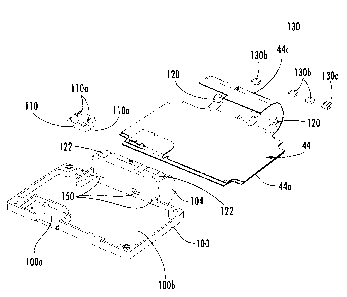
FIG. 3 is an exploded isometric view of the main circuit board 67, the
keyboard
support 100, which would be carried by the housing 21 within the lower portion
47. The
keyboard support 100 has a substantially planar keyboard section 102 and
antenna support
section 104. The keyboard circuit board 44 is supported by the keyboard
support 100 and,
as noted before, includes a keyboard section 44a and keyboard circuitry 44b
thereon, such
as the illustrated integrated domes 44e. The keyboard circuitry 44b connects
to circuitry
48 on the main circuit board 67 using a compression connector 110 that is
supported by
the underside of the keyboard support 100 as shown in FIGS. 5 and 6. It has
connecting
posts 110a that could connect to the main circuit board 67 and allow
interconnection of
circuitry 48 on the main circuit board to keyboard circuitry 44b. As shown in
FIG. 6, the
compression connector 110 is fitted within a receiving slot 100a on the
underside 100b of
the keyboard support 100.
FIG. 4 shows the keyboard support 100, main circuit board 67 and keyboard
circuit
board 44 connected together. As illustrated, the main circuit board 67 has a
lower portion
67a and the antenna section 44c of the keyboard circuit board 44 and the
antenna support
section 104 straddles both sides of the lower portion of the main circuit
board, although
this is not required. This design is beneficial because prior art designs
typically used a
main circuit board that was positioned on only one side of an internal
antenna. The
structure shown in FIG. 4 allows greater flexibility in antenna design and
allows the use of
larger patterns and new antenna geometries because it offers the ability to
place the
antenna elements much farther apart than some previous designs. The antenna
configuration can also allow beam shaping.
The circuitry 48 on the main circuit board can also be disposed on one side or
both
sides. One side can be preferred because this facilitates assembly and
preserves a single-
sided radio board construction. It is thus self aligning and self correcting,
and the
keyboard circuit board 44 can be snapped into place with the keyboard support
100 and
the main circuit board 67.
Contact arms 120 formed similar to springs as extensions or cuts are
preferably
formed on the antenna section 44c and engage the keyboard support 100 to aid
in securing
together the keyboard circuit board 44 and keyboard support 100. These contact
arms 120
are formed similar to springs as shown in FIG. 5 and engage receiving slots
122 in the
antenna support section of the keyboard support 100 to aid in securing
together the
keyboard circuit board 44 and keyboard support 100.
CA 02528030 2005-12-22
FIG. 3 shows various support alignment holes 123 in the main circuit board and
locating posts 124 on the keyboard support 100 to align the main circuit board
and
keyboard support together. Conductive contacts 130 are positioned on the
antenna section
44c and interconnect conductive traces forming the antenna circuit to
circuitry 67 on the
main circuit board. In one aspect of the invention, the conductive contacts
130 comprise a
spring contact or finger that could be formed as a mechanical spring 130a or
conductive
elastomeric pad 130b, such as shown in FIGS. 3 and 5. It is evident that the
single flex
circuit forming the keyboard circuit board 44 contains both the antenna
geometry and the
electrical network necessary for the keyboard. There is a selective
metallization and
circuitry to form the antenna pattern. In one aspect of the present invention,
the keyboard
support 100 can be formed from plastic or other similar, but lightweight rigid
material.
The keyboard support 100 and main circuit board 67 each include guide and/or
mounting
holes 135 at each corner that receive fasteners or other guide pins to align
or secure the
assembled structure such as shown in FIG. 4 within the housing.
FIGS. 7-9 show the assembly of the keyboard support 100, main circuit board 67
and keyboard circuit board 49 and the insertion direction of the various
components by the
arrow at 140.
During assembly, contact fingers 87b positioned on the main circuit board
engage
the conductive contacts 130 through receiving openings 150 formed on the
underside 100b
of the antenna support section 104, as shown in FIG. 6. The contact fingers
87b include
portions of the circuitry 48 and pass through the openings and allow the
interconnection of
electrical circuitry on the main circuit board with the conductive traces
forming an antenna
circuit. The fingers 87b on the main circuit board extend into the openings
150, and when
assembled, engage the conductive arms 120 positioned on the antenna section to
allow
interconnection of conductive traces for the antenna circuit to circuitry on
the main circuit
board. The spring finger or elastomeric pad 130 is also shown in detail in
FIG. 7 to ensure
connection of the antenna circuit to the circuitry on the main circuit board.
A flex tail 136
is shown in an undeflected 136' and deflected position 136.
Another example of a hand-held mobile wireless communications device 1000 that
may be used in accordance the present invention is further described in the
example below
with reference to FIG. 10. The device 1000 illustratively includes a housing
1200, a
keypad 1400 and an output device 1600. 'The output device shown is a display
1600,
which is preferably a full graphic LCD. Other types of output devices may
alternatively be
11
CA 02528030 2005-12-22
utilized. A processing device 1800 is contained within the housing 1200 and is
coupled
between the keypad 1400 and the display 1600. The processing device 1800
controls the
operation of the display 1600, as well as the overall operation of the mobile
device 1000,
in response to actuation of keys on the keypad 1400 by the user.
The housing 1200 may be elongated vertically, or may take on other sizes and
shapes (including clamshell housing structures). The keypad may include a mode
selection
key, or other hardware or software for switching between text entry and
telephony entry.
In addition to the processing device 1800, other parts of the mobile device
1000 are
shown schematically in FIG. 10. These include a communications subsystem 1001;
a
short-range communications subsystem 1020; the keypad 1400 and the display
1600,
along with other inputloutput devices 1060, 1080, 1100 and 1120; as well as
memory
devices 1160, 1180 and various other device subsystems 1201. The mobile device
1000 is
preferably a two-way RF communications device having voice and data
communications
capabilities. In addition, the mobile device 1000 preferably has the
capability to
communicate with other computer systems via the Internet.
Operating system software executed by the processing device 1800 is preferably
stored in a persistent store, such as the flash memory 1160, but may be stored
in other
types of memory devices, such as a read only memory (ROM) or similar storage
element.
In addition, system software, specific device applications, or parts thereof,
may be
temporarily loaded into a volatile store, such as the random access memory
(RAM) 1180.
Communications signals received by the mobile device may also be stored in the
RAM
1180.
The processing device 1800, in addition to its operating system functions,
enables
execution of software applications 1300A-1300N on the device 1000. A
predetermined set
of applications that control basic device operations, such as data and voice
communications 1300A and 1300B, may be installed on the device 1000 during
manufacture. In addition, a personal information manager (PIM) application may
be
installed during manufacture. The PIM is preferably capable of organizing and
managing
data items, such as e-mail, calendar events, voice mails, appointments, and
task items. The
PIM application is also preferably capable of sending and receiving data items
via a
wireless network 1401. Preferably, the PIM data items are seamlessly
integrated,
synchronized and updated via the wireless network 1401 with the device user's
corresponding data items stored or associated with a host computer system.
12
CA 02528030 2005-12-22
Communication functions, including data and voice communications, are
performed through the communications subsystem 1001, and possibly through the
short-
range communications subsystem. The communications subsystem 1001 includes a
receiver 1500, a transmitter 1520, and one or more antennas 1540 and 1560. In
addition,
the communications subsystem 1001 also includes a processing module, such as a
digital
signal processor (DSP) 1580, and local oscillators (LOs) 1601. The specific
design and
implementation of the communications subsystem 1001 is dependent upon the
communications network in which the mobile device 1000 is intended to operate.
For
example, a mobile device 1000 may include a communications subsystem 1001
designed
to operate with the MobitexTM, Data TACTM or General Packet Radio Service
(GPRS)
mobile data communications networks, and also designed to operate with any of
a variety
of voice communications networks, such as AMPS, TDMA, CDMA, PCS, GSM, etc.
Other types of data and voice networks, both separate and integrated, may also
be utilized
with the mobile device 1000.
Network access requirements vary depending upon the type of communication
system. For example, in the Mobitex and DataTAC networks, mobile devices are
registered on the network using a unique personal identification number or PIN
associated
with each device. In GPRS networks, however, network access is associated with
a
subscriber or user of a device. A GPRS device therefore requires a subscriber
identity
module, commonly referred to as a SIM card, in order to operate on a GPRS
network.
When required network registration or activation procedures have been
completed,
the mobile device 1000 may send and receive communications signals over the
communication network 1401. Signals received from the communications network
1401
by the antenna 1540 are routed to the receiver 1500, which provides for signal
amplification, frequency down conversion, filtering, channel selection, etc.,
and may also
provide analog to digital conversion. Analog-to-digital conversion of the
received signal
allows the DSP 1580 to perform more complex communications functions, such as
demodulation and decoding. In a similar manner, signals to be transmitted to
the network
1401 are processed (e.g. modulated and encoded) by the DSP 1580 and are then
provided
to the transmitter 1520 for digital to analog conversion, frequency up
conversion, filtering,
amplification and transmission to the communication network 1401 (or networks)
via the
antenna 1560.
13
CA 02528030 2005-12-22
In addition to processing communications signals, the DSP 1580 provides for
control of the receiver 1500 and the transmitter 1520. For example, gains
applied to
communications signals in the receiver 1500 and transmitter 1520 may be
adaptively
controlled through automatic gain control algorithms implemented in the DSP
1580.
In a data communications mode, a received signal, such as a text message or
web
page download, is processed by the communications subsystem 1001 and is input
to the
processing device 1800. The received signal is then further processed by the
processing
device 1800 for an output to the display 1600, or alternatively to some other
auxiliary I/O
device 1060. A device user may also compose data items, such as e-mail
messages, using
the keypad 1400 and/or some other auxiliary I/O device 1060, such as a
touchpad, a rocker
switch, a thumb-wheel, or some other type of input device. The composed data
items may
then be transmitted over the communications network 1401 via the
communications
subsystem 1001.
In a voice communications mode, overall operation of the device is
substantially
similar to the data communications mode, except that received signals are
output to a
speaker 1100, and signals for transmission are generated by a microphone 1120.
Alternative voice or audio I/O subsystems, such as a voice message recording
subsystem,
may also be implemented on the device 1000. In addition, the display 1600 may
also be
utilized in voice communications mode, for example to display the identity of
a calling
party, the duration of a voice call, or other voice call related information.
The short-range communications subsystem enables communication between the
mobile device 1000 and other proximate systems or devices, which need not
necessarily be
similar devices. For example, the short-range communications subsystem may
include an
infrared device and associated circuits and components, or a BluetoothTM
communications
module to provide for communication with similarly-enabled systems and
devices.
Many modifications and other embodiments of the invention will come to the
mind
of one skilled in the art having the benefit of the teachings presented in the
foregoing
descriptions and the associated drawings. Therefore, it is understood that the
invention is
not to be limited to the specific embodiments disclosed, and that
modifications and
embodiments are intended to be included within the scope of the appended
claims.
14