Language selection

Search

Patent 2528051 Summary

Third-party information liability

Some of the information on this Web page has been provided by external sources. The Government of Canada is not responsible for the accuracy, reliability or currency of the information supplied by external sources. Users wishing to rely upon this information should consult directly with the source of the information. Content provided by external sources is not subject to official languages, privacy and accessibility requirements.

Claims and Abstract availability

Any discrepancies in the text and image of the Claims and Abstract are due to differing posting times. Text of the Claims and Abstract are posted:

  • At the time the application is open to public inspection;
  • At the time of issue of the patent (grant).
(12) Patent: (11) CA 2528051
(54) English Title: SYSTEM AND METHOD FOR REFORMATTING DATA
(54) French Title: SYSTEME ET PROCEDE DESTINES AU REFORMATAGE DE DONNEES
Status: Expired and beyond the Period of Reversal
Bibliographic Data
(51) International Patent Classification (IPC):
  • G06F 05/10 (2006.01)
  • H04L 12/20 (2006.01)
(72) Inventors :
  • ESHRAGHIAN, HAMED (United States of America)
(73) Owners :
  • CISCO TECHNOLOGY, INC.
(71) Applicants :
  • CISCO TECHNOLOGY, INC. (United States of America)
(74) Agent: SMART & BIGGAR LP
(74) Associate agent:
(45) Issued: 2013-01-22
(86) PCT Filing Date: 2004-06-03
(87) Open to Public Inspection: 2004-12-16
Examination requested: 2009-01-22
Availability of licence: N/A
Dedicated to the Public: N/A
(25) Language of filing: English

Patent Cooperation Treaty (PCT): Yes
(86) PCT Filing Number: PCT/US2004/017287
(87) International Publication Number: US2004017287
(85) National Entry: 2005-12-02

(30) Application Priority Data:
Application No. Country/Territory Date
60/475,521 (United States of America) 2003-06-03

Abstracts

English Abstract


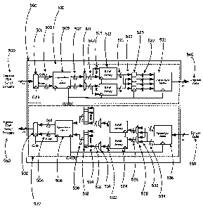
A converter for converting serial (e.g. TDM) data streams into parallel (e.g.
cell) data is presented. Conversion from cell to TDM format is also disclosed.
Methods for converting between serial and parallel data formats are provided.
In some applications communication data streams of digital data may be
captured, processed, and stored in one or more of the serial and cell data
formats.


French Abstract

L'invention concerne un convertisseur destiné à la conversion de flux de données sérielles (p.ex., de TDM) en données parallèles. Elle concerne également la conversion du format cellules au format TDM ainsi que des procédés de conversion entre les formats de données sérielles et parallèles. Dans certaines applications, des flux de données de communication de données numériques peuvent être capturés, traités et stockés dans un ou plusieurs formats de données de cellules ou sérielles.

Claims

Note: Claims are shown in the official language in which they were submitted.


CLAIMS
1. A system for formatting data comprising:
an input processor, receiving data from at least one stream of data at a first
clock
rate in a serial fashion, and providing an input processor output at a second
clock rate in a
serial fashion, wherein the second clock rate is faster than the first clock
rate;
a memory array operating at the second clock rate, receiving the output of the
input processor in a serial fashion and providing a memory array output in a
parallel
fashion; and
a register operating at the second clock rate, taking the memory array output
and
providing a plurality of bits in parallel corresponding to a known format.
2. The system of claim 1, wherein the input processor is an asynchronous
queue.
3. The system of claim 2, further comprising a multiplexer disposed between
the
asynchronous queue and the memory array.
4. The system of claim 1 or claim 2, wherein the memory array comprises at
least one
RAM device including a plurality of bit places.
5. The system of any one of claims 1 to 4, further comprising a synchronous
queue that
receives the plurality of bits from the register and provides a data cell of
output bits.
6. The system of any one of claims 1 to 5, wherein the at least one stream of
data
comprises serial time division multiplexed TDM data.
7. The system of any one of claims 1 to 6, further comprising:
a second memory array, receiving data in the known format in a parallel
fashion
and providing a memory array output in a serial fashion; and
an output processor coupled to the second memory array that receives input in
a
serial fashion at the second clock rate and outputs a data stream at the first
clock rate and
in a second format.
8

8. A method for formatting data comprising:
receiving data from at least one stream of data at a first clock rate in a
serial
fashion into an asynchronous queue, and providing an asynchronous queue output
at a
second clock rate in a serial fashion from the asynchronous queue, wherein the
second
clock rate is faster than the first clock rate;
placing the output of the asynchronous queue into a memory array in a serial
fashion and at the second clock rate, and providing a memory array output from
the
memory array in a parallel fashion; and
receiving the memory array output at a register operating at the second clock
rate,
and providing from the register a plurality of bits in parallel corresponding
to a known
format.
9. The method of claim 8, further comprising:
receiving data in the known format and in a parallel fashion; and
converting the data into a second format and from a parallel fashion to a
serial
fashion for output.
10. The method of claim 8 or claim 9, further comprising multiplexing one or
more data
streams output from the asynchronous queue.
11. The method of any one of claims 8 to 10, further comprising receiving the
plurality of
bits from the register at a synchronous queue and providing a data cell of
output bits.
12. The method of any one of claims 8 to 11, wherein the plurality of bits in
parallel
corresponding to the known format includes identification information of a
cell number.
13. The method of any one of claims 8 to 12, wherein the at least one stream
of data are
digital voice data streams on a communication network.
14. The method of any one of claims 8 to 13, wherein the method is implemented
on a
chassis responsible for at least one of receiving, forwarding and processing
data streams
on a digital voice communication network.
9

15. A system for formatting data comprising:
an input processor that receives a plurality of input serial data streams at a
first clock
rate and outputs a plurality of bits corresponding to the input serial data
streams at a
second clock rate, said second clock rate being greater than said first clock
rate;
a multiplexer taking an input from the output of the input processor and
providing a
sequential multiplexer output;
a memory array sequentially taking an input from the output of the
multiplexer;
a register coupled to the memory array and adapted to read data content from
the
memory array in parallel; and
an output processor that receives the at least one word of data content from
the
register in parallel and produces a cell formatted word of data corresponding
to the
plurality of input serial data streams.
16. The system of claim 15, wherein the input processor includes an
asynchronous queue
and the output processor includes a synchronous queue.
17. The system of claim 15 or 16, wherein the plurality of streams of serial
data are
digital voice data streams on a communication network.
18. The system of any one of claims 15 to 17, wherein the input processor,
multiplexer,
memory array, register and output processor are implemented in a chassis
responsible for
at least one of receiving, forwarding and processing data streams on a digital
voice
communication network.
19. The system of any one of claims 1 to 7, wherein the plurality of bits in
parallel
corresponding to the known format is used on a chassis responsible for at
least one of
receiving, forwarding and processing data streams on a digital voice
communication
network.
20. The system of any one of claim 1 to 7 and claim 19, wherein the at least
one stream of
data are digital voice data streams on a communication network.

21. A system comprising:
a first interface receiving a first clock signal at a first clock rate;
a second interface receiving a second clock signal at a second clock rate;
an asynchronous queue, receiving a first clock signal from the first interface
and the
second clock signal from the second interface, receiving data from a plurality
of streams
of serial TDM data at the first clock rate, and providing a parallel
asynchronous queue
output at the second clock rate;
a multiplexer receiving the parallel asynchronous queue output and providing a
serial
multiplexer output;
a memory array, receiving the output of the multiplexer in a serial fashion
and providing
a memory array output in a parallel fashion; and
a register, receiving the clock signal from the second interface, taking the
memory array
output and providing a plurality of bits in parallel corresponding to the data
cell format at
the second clock rate.
22. The system of claim 1, wherein the second clock rate is faster than the
first clock
rate.
23. The system of claim 1, wherein the memory array comprises at least one RAM
device including a plurality of bit places.
24. The system of claim 1, further comprising a synchronous queue that
receives the
plurality of bits from the register and provides a data cell of output bits.
11

25. The system of claim 1, wherein the parallel asynchronous queue output
includes
bits from each of the plurality of streams of data corresponding to a channel
and the serial
multiplexer output includes at least one word of data corresponding to the
bits
multiplexed in a serial fashion.
26. A method comprising:
receiving serial TDM data from a plurality of streams of serial TDM data at a
first clock
rate into an asynchronous queue, and providing a parallel asynchronous queue
output at a
second clock rate from the asynchronous queue;
multiplexing the parallel asynchronous queue output and providing a serial
multiplexer
output;
placing the serial multiplexer output into a memory array in a serial fashion,
and
providing a memory array output from the memory array in a parallel fashion at
the
second clock rate;
receiving the memory array output at a register;
providing from the register a plurality of bits in parallel at the second
clock rate; and
providing the plurality of bits in parallel synchronously as output bits.
27. A system comprising:
a first interface receiving a first clock signal at a first clock rate;
a second interface receiving a second clock signal at a second clock rate;
an input processor, receiving the first clock signal from the first interface
and the second
clock signal from the second interface, that receives a plurality of input
serial data
streams at the first clock rate and outputs a plurality of bits corresponding
to the input
serial data streams at the second clock rate, the second clock rate being
greater than the
first clock rate;
12

a multiplexer taking an input from the output of the input processor and
providing a
sequential multiplexer output;
a memory array sequentially taking an input from the output of the
multiplexer;
a register coupled to the memory array and the second interface and adapted to
read at
least one word of data content from the memory array in parallel; and
an output processor that receives at least one word of data content from the
register in
parallel and produces a cell formatted word of data at the second clock rate
corresponding
to the plurality of input serial data streams.
28. The method of claim 26, wherein the second clock rate is faster than the
first clock rate.
29. The method of claim 26, further comprising the parallel asynchronous queue
output.
30. The method of claim 26, further comprising receiving the plurality of bits
at a
synchronous queue from the register and providing a data cell of output bits.
31. The method of claim 27, wherein the plurality of bits in parallel at the
second
clock rate includes identification information of a cell number.
32. The system of claim 27, wherein the input processor includes an
asynchronous
queue and the output processor includes a synchronous queue.
33. The system of claim 21, wherein the plurality of streams of serial TDM
data are digital voice data streams on a communication network.
34. The method of claim 26, wherein the plurality of streams of serial TDM
data are digital voice data streams on a communication network.
13

35. The system of claim 27, wherein the plurality of input serial data streams
are
digital voice data streams on a communication network.
36. The method of claim 21, wherein the method is implemented on a chassis
responsible for at least one of receiving, forwarding and processing data
streams on a
digital voice communication network.
37. The system of claim 27, wherein the input processor, multiplexer, memory
array,
register and output processor are implemented in a chassis responsible for at
least one of
receiving, forwarding and processing data streams on a digital voice
communication
network.
38. The system of claim 21, wherein the plurality of bits in parallel
corresponding to
the data cell format is used on a chassis responsible for at least one of
receiving,
forwarding and processing data streams on a digital voice communication
network.
14

Description

Note: Descriptions are shown in the official language in which they were submitted.


CA 02528051 2005-12-02
WO 2004/109997 PCT/US2004/017287
SYSTEM AND METHOD FOR REFORMATTING DATA
TECHNICAL FIELD
[0001] The present application generally relates to data processing, and more
particularly, to systems and techniques for reformatting digital data.
BACKGROUND
[0002] In digital communication applications, for example, Time Division
Multiplexing (TDM) systems, voice data is converted from analog to digital
form, and
binary digits (bits) are sent over a communication network. The bits of
digitized voice
data are streamed serially over multiple physical communication network lines
in
organized formats, understandable to devices coupled to the communication
network
lines.
[0003] Figure 1 illustrates an example of TDM communication data in which
serial
streams of digital voice data 100 are carried over a number of communication
lines. Each
line or stream 100 is logically divided into a sequence of frames 110, and
each frame 110
includes a sequence of channels 120. Information is delivered from source to
destination
using bytes 102, each of which includes 8 bits 104 of data. A frame 110
contains 128
channels 120. The channels 120 are designated Channel 0, Channel 1, ...,
Channel 126,
and Channel 127. A given telephone conversation will occupy one of the
channels, e.g.
Channel 1 of Stream No. 2. Note that each channel is allotted one byte in each
frame 110
of its stream. Therefore, a conversation carried on a channel (e.g. Channel 1)
is
segmented into byte-sized parts that share a same stream (e.g. Stream No. 2)
as 127 other
conversations occupying the other 127 channels in the stream. In all, a system
carrying
24 streams of data can handle (24 streams x 128 conversations/stream) = 3072
conversations at the same time, albeit not continuous. That is, for each
streaming frame
of data 110, 128 conversations are being carried (in real time to their
participants) but are
physically sharing the frame 110 among the 128 channels 120. In one example,
the data
transmission frequency is 8.192 MHz with a period of 122 nsec.
[0004] While TDM is a popular format for data transmission, it is not always
possible
or convenient to receive digitized voice data according to the TDM serial
streaming
format described above. In some cases the hardware receiving, forwarding, or
processing

CA 02528051 2005-12-02
WO 2004/109997 PCT/US2004/017287
the data streams is not adapted for the TDM format. Accordingly, for any of
several
reasons, it may be desirable to reformat the digital voice data streams into
another useful
format.
SUMMARY
[0005] One aspect of the present disclosure is directed to a system for
converting at
least one stream of data into a data cell format, including an asynchronous
queue,
receiving data from the at least one stream of data at a first clock rate, and
providing an
asynchronous queue output at a second clock rate; a memory array receiving the
output of
the asynchronous queue and providing a memory array output; and a register
taking the
memory array output and providing a plurality of bits in parallel
corresponding to the data
cell format.
[0006] Another aspect of the present disclosure is directed to a method for
converting
at least one stream of data into a data cell format, receiving data from the
at least one
stream of data at a first clock rate into an asynchronous queue, and providing
an
asynchronous queue output at a second clock rate from the asynchronous queue;
placing
the output of the asynchronous queue into a memory array, and providing a
memory array
output from the memory array; and receiving the memory array output at a
register, and
providing from the register a plurality of bits in parallel corresponding to
the data cell
format.
[0007] Yet another aspect of the present disclosure is directed to a converter
for
converting data from a first format into a second format, elements for
receiving at least
one stream of serial data corresponding to the first data format; elements for
storing the at
least one stream of serial data, a plurality of bits of the stream of serial
data being stored
in parallel; and
elements for reading the stored data in the storing elements onto a parallel
bus
corresponding to the second data format.
BRIEF DESCRIPTION OF THE DRAWINGS
[0008] For a fuller understanding of the nature and objects of the present
disclosure,
reference should be made to the following detailed description, in connection
with the
2

CA 02528051 2005-12-02
WO 2004/109997 PCT/US2004/017287
accompanying drawings, in which the same reference numerals are used to
indicate the
same or similar parts, wherein:
Figure 1 illustrates several frames of serial TDM data according to the
related
art;
Figure 2 illustrates an exemplary embodiment of a serial-to-cell and cell-to-
serial converter according to the present invention;
Figure 3 illustrates an arrangement of RAM array devices;
Figure 4 illustrates an exemplary data cell format; and
Figure 5 illustrates an exemplary arrangement of data according to a read-
write configuration of the RAM arrays.
DETAILED DESCRIPTION
[0009] As discussed briefly above, TDM voice data is transmitted in serial
streams on
a plurality of fines. A system and method for reformatting the TDM data into
another
useful format is presented in detail below, and specifically with reference to
a particular
exemplary embodiment. It should be appreciated that other formats and
embodiments are
also possible using the same inventive principles, and such modifications and
extensions
may be comprehended by those practiced in the field.
[0010] Figure 2 is a block diagram of an exemplary embodiment of a system for
converting serial TDM streams into cell data blocks, and cell data blocks into
serial TDM
streams. Separate parts of the system 500 can be used for achieving each type
of
reformatting. In the present example, circuit 510 reformats the data from
serial TDM
streams into parallel cell format, and circuit 520 reformats data from
parallel cell format
into serial TDM format. Each of the parts 510, 520 of the system 500 could be
implemented separately or disposed on individual circuit boards or integrated
circuits.
The system 500 is suited for use in a communication system that interacts with
other
systems using the TDM format, whereby TDM streams arrive at the ingress 530,
are
converted to cell format, processed, then returned to TDM streams that are
sent out the
TDM egress path 560.
[0011] Circuit 510 converts data arriving in TDM stream format at ingress 530
to cell
format at ingress cell path line 540. As described earlier with respect to
Figure 1, 24
streams of TDM data (in 24 separate serial streams) are presented at TDM
ingress 530.

CA 02528051 2005-12-02
WO 2004/109997 PCT/US2004/017287
This is graphically represented in Figure 2 by the slash and the numeral "24"
on the
ingress line. The incoming data at 530 is presented at a clock "CLKB"
frequency of 8.192
MHz, i.e., 24 bits arrive every 122 nsec. Deinterleaver 501 provides two 12-
bit streams
of data 503, one stream being for the odd numbered streams and another stream
for the
even numbered input streams. The odd and even bit streams are placed into
ingress
asynchronous queue 505.
[0012] Operations downstream of the ingress asynchronous queue 505 are carried
out
at a higher frequency of 100 MHz ("CLK 100"). The 12-bit wide odd and even
streams
507, now clocked at 100 MHz, are multiplexed by multiplexers 511 to provide a
corresponding pair of single output streams 513 that are delivered to RAM
arrays 517
through parallel inputs 515. The first words read contain bit 7 of channel 0
of each of the
24 incoming TDM streams, and are written to sequential addresses of RAM array
517 at
bit position 6. The next words read contain bit 6 of channel 0 of all 24 TDM
streams, and
are also written to sequential addresses of RAM array 517 at bit position 6.
This process
is repeated until bits 0 of the TDM streams are written to sequential
addresses of RAM
array 517 at bit position 0. Therefore, the TDM serial data at 530, which is
taken in by
circuit 510 at 8 MHz, is delivered to RAM arrays 517 in serial fashion at 100
MHz.
RAM arrays 517 will be discussed in more detail below, and in some embodiments
provide space, cost, and other design savings and formatting advantages over
traditional
flip-flop designs for converting data from a serial to a parallel format.
[0013] Using RAM arrays 517 provides a cost and space saving, which can be
important in integrated circuit applications. To perform the functions
described above
without the RAM arrays 517 of the present invention, 96 flip-flops (12x8)
would be
required for each RAM array according to conventional design methods. However,
the
footprint of the RAM arrays 517 is much smaller, and is equivalent to the
footprint of
about 8 flip-flops only, providing a substantial area savings according to the
present
illustrative example. The RAM arrays may be loaded serially (written) and then
read in
parallel. Of course, this process is adaptable for sizes of arrays and words
other than
those given in this example.
[0014] RAM arrays 517 output odd and even bytes 521 to register 525, and the
contents of all RAM arrays 517 are read in parallel, and the bytes from the
odd and even
sections are combined to form a 16-bit word. This word is combined with the
output of
4

CA 02528051 2005-12-02
WO 2004/109997 PCT/US2004/017287
the following RAM read to create a 32-bit word that is sent to ingress
synchronous queue
531 using register 525. Register 525 is a 32-bit (8x4) register, clocked at
100 MHz, and
provides 32 bits in parallel to ingress synchronous queue 531. Ingress
synchronous queue
531 then outputs a 32-bit wide parallel cell of data at ingress cell path 540.
The ingress
cell path 540 can be used to provide cell data to components of a
communication system
that processes data in cell format rather that TDM format. When such a
communication
system has received or processed the cell data, it may return the cell format
data to an
external network in TDM serial format using parallel-to-serial circuit 520.
[0015] Circuit 520 receives as input egress cells 550, which are 32-bit wide
parallel
cells written into egress synchronous queue 536 at 100 MHz. Odd and even
groups of
bytes 534 are provided to multiplexes pair 528. Multiplexers 528 output bytes
of data 526
to a pair of RAM arrays 524. The bytes associated with odd and even streams
are
separated and axe written to RAM arrays 524 with a similar placement of bits
as was used
in the ingress RAM array 517 paths. Each of the two 16x1 RAM word
corresponding to
bit 7 is then read out starting at address 0 and ending at address 11, thus
providing bit 7 of
channel 0 for each of the 24 data streams. This process is repeated for the
remaining 7
RAM pairs in RAM arrays 524.
[0016] RAM arrays 524 output two bytes of data 522, which are multiplexed by
multiplexers 518 into two corresponding 1-bit streams 516. The 1-bit streams
516 are
provided through 12 line pairs 514 to 12-bit registers 512. Registers 512,
clocked at 100
MHz, provide two 12-bit outputs to egress asynchronous queue 506. The cell
number,
embedded in each cell, is compared with a local counter that tracks the number
of the
next cell that must be output. If there is no match or the next cell has not
arrived yet,
OxFF is sent out for both channels on all 24 streams and an interrupt is
generated. Egress
asynchronous queue 506 then outputs the two sets (odd, even) of 12 bit data at
8MHz
onto output lines 504. An interleaves 502 places the 24 bits of data (12 odd,
12 even) in
the proper order onto egress TDM serial stream lines 560, which is available
to as 24
frames to a TDM serial communication system. The TDM serial streams may be
sent
through digital switches to voice processing systems.
[0017] The entire system 500 may be constructed in a field programmable gate
array
(FPGA) device, or may be otherwise assembled from electronic components on one
or
more circuit boards or integrated circuits. Also, the system may be enhanced
or

CA 02528051 2005-12-02
WO 2004/109997 PCT/US2004/017287
augmented through the use of other auxiliary circuits and systems (not shown)
and
accompanying software to operate, control, and process data through the
system.
[0018] Figure 3 illustrates RAM arrays 517, 524, whose function was described
above. The RAM arrays 517, 524 in this example are 8-bits wide by 16-bits
deep.
Compared to equivalent flip-flops, a RAM device takes up less space, and has
its
addressing functionality built into the RAM array rather than being external
to the device,
as in a flip-flop array. Eight RAM devices 610 are packaged in each RAM array
517,
524. The lines labeled "A" are a 4-bit addressing input to the array; the
lines labeled
"WE" indicate write-enable; the lines labeled "WD" indicate write-data; and
the lines
labeled "RD" indicate read-data. The RAM array also takes a clock "CLK" input
(at 100
MHz in the present example). The fact that there are 12 10-nsec cycles of the
fast (100
MHz) clock within the 122-nsec period of the slower (8.192 MHz) clock allows
the steps
described to be carried out on the 24 sets of incoming TDM frames in real
time.
[0019] Figure 4 illustrates an exemplary data cell format according to one
embodiment compatible with the present invention. Each cell 700 carries two
channels/bytes of data 720, 730 from each of the incoming 24 TDM data streams.
One
TDM frame is therefore carried by 64 cells according to the present exemplary
cell
format. In the figure, "ST" denotes a stream number, and "CH" denotes a
channel
number within the stream, with "n" being an even number starting with "0". A 2-
bit
frame number and a 6-bit cell number identifying the cell within the frame are
provided
in the first byte (byte 0).
[0020] Figure 5 illustrates an exemplary bit placement table for bits in the
RAM
arrays 517, 524. The cells are written as multiple 32-bit words into the
egress
synchronous queue 536. The table 800 corresponds to the hardware described in
the
previous figures, and includes 12 rows 810 and 8 columns 820. The table is
filled with
the data as indicated by the stream "ST" and Bit numbers, with the order of
filling being
in columns, from top to bottom (12 bits 830). Conversely, the RAM arrays are
read in
rows from left to right (8 bits 840).
[0021] The system described above in one exemplary embodiment, and the methods
for reading, storing, and writing data from a serial TDM stream format to a
cell format
and back to a serial TDM format are useful in communication applications in
which TDM
and cell formats are used, and conversion from one form to the other is
accomplished. It
6

CA 02528051 2005-12-02
WO 2004/109997 PCT/US2004/017287
should be understood that the examples provided are not limiting or inclusive,
but rather,
the invention, as given by the claims which follow comprehends numerous
modifications
and augmentations within the same scope.
What is claimed is:
7

Representative Drawing
A single figure which represents the drawing illustrating the invention.
Administrative Status

2024-08-01:As part of the Next Generation Patents (NGP) transition, the Canadian Patents Database (CPD) now contains a more detailed Event History, which replicates the Event Log of our new back-office solution.

Please note that "Inactive:" events refers to events no longer in use in our new back-office solution.

For a clearer understanding of the status of the application/patent presented on this page, the site Disclaimer , as well as the definitions for Patent , Event History , Maintenance Fee  and Payment History  should be consulted.

Event History

Description Date
Time Limit for Reversal Expired 2018-06-04
Letter Sent 2017-06-05
Revocation of Agent Requirements Determined Compliant 2017-03-28
Appointment of Agent Requirements Determined Compliant 2017-03-28
Revocation of Agent Request 2017-02-24
Appointment of Agent Request 2017-02-24
Grant by Issuance 2013-01-22
Inactive: Cover page published 2013-01-21
Inactive: IPC assigned 2013-01-08
Inactive: First IPC assigned 2013-01-08
Inactive: IPC assigned 2013-01-08
Inactive: IPC expired 2013-01-01
Inactive: IPC removed 2012-12-31
Pre-grant 2012-11-14
Inactive: Final fee received 2012-11-14
Notice of Allowance is Issued 2012-05-28
Letter Sent 2012-05-28
Notice of Allowance is Issued 2012-05-28
Inactive: Approved for allowance (AFA) 2012-05-24
Amendment Received - Voluntary Amendment 2012-03-30
Amendment Received - Voluntary Amendment 2012-03-23
Inactive: S.30(2) Rules - Examiner requisition 2012-02-08
Amendment Received - Voluntary Amendment 2011-12-09
Letter Sent 2011-12-07
Inactive: S.30(2) Rules - Examiner requisition 2011-06-09
Amendment Received - Voluntary Amendment 2011-04-15
Amendment Received - Voluntary Amendment 2011-04-07
Amendment Received - Voluntary Amendment 2011-04-06
Inactive: S.30(2) Rules - Examiner requisition 2010-10-07
Inactive: Adhoc Request Documented 2010-09-01
Inactive: Office letter 2010-09-01
Inactive: Delete abandonment 2010-09-01
Revocation of Agent Request 2010-07-09
Inactive: Multiple transfers 2010-07-09
Appointment of Agent Request 2010-07-09
Revocation of Agent Requirements Determined Compliant 2010-07-05
Inactive: Office letter 2010-07-05
Appointment of Agent Requirements Determined Compliant 2010-07-05
Letter Sent 2010-06-29
Amendment Received - Voluntary Amendment 2010-06-10
Deemed Abandoned - Failure to Respond to Maintenance Fee Notice 2010-06-03
Revocation of Agent Request 2010-06-01
Appointment of Agent Request 2010-06-01
Amendment Received - Voluntary Amendment 2009-07-20
Letter Sent 2009-02-19
Amendment Received - Voluntary Amendment 2009-01-22
Request for Examination Requirements Determined Compliant 2009-01-22
All Requirements for Examination Determined Compliant 2009-01-22
Request for Examination Received 2009-01-22
Letter Sent 2008-07-16
Reinstatement Requirements Deemed Compliant for All Abandonment Reasons 2008-06-18
Deemed Abandoned - Failure to Respond to Maintenance Fee Notice 2008-06-03
Letter Sent 2007-01-05
Inactive: Applicant deleted 2007-01-04
Inactive: Correspondence - Transfer 2006-12-13
Correct Applicant Request Received 2006-12-04
Inactive: Single transfer 2006-12-04
Inactive: Cover page published 2006-02-10
Inactive: Courtesy letter - Evidence 2006-02-07
Inactive: Notice - National entry - No RFE 2006-02-06
Application Received - PCT 2006-01-12
National Entry Requirements Determined Compliant 2005-12-02
Application Published (Open to Public Inspection) 2004-12-16

Abandonment History

Abandonment Date Reason Reinstatement Date
2010-06-03
2008-06-03

Maintenance Fee

The last payment was received on 2012-05-25

Note : If the full payment has not been received on or before the date indicated, a further fee may be required which may be one of the following

  • the reinstatement fee;
  • the late payment fee; or
  • additional fee to reverse deemed expiry.

Patent fees are adjusted on the 1st of January every year. The amounts above are the current amounts if received by December 31 of the current year.
Please refer to the CIPO Patent Fees web page to see all current fee amounts.

Owners on Record

Note: Records showing the ownership history in alphabetical order.

Current Owners on Record
CISCO TECHNOLOGY, INC.
Past Owners on Record
HAMED ESHRAGHIAN
Past Owners that do not appear in the "Owners on Record" listing will appear in other documentation within the application.
Documents

To view selected files, please enter reCAPTCHA code :


To view images, click a link in the Document Description column. To download the documents, select one or more checkboxes in the first column and then click the "Download Selected in PDF format (Zip Archive)" or the "Download Selected as Single PDF" button.

List of published and non-published patent-specific documents on the CPD .

If you have any difficulty accessing content, you can call the Client Service Centre at 1-866-997-1936 or send them an e-mail at CIPO Client Service Centre.


Document
Description 
Date
(yyyy-mm-dd) 
Number of pages   Size of Image (KB) 
Description 2005-12-01 7 358
Drawings 2005-12-01 5 114
Representative drawing 2005-12-01 1 20
Claims 2005-12-01 2 76
Abstract 2005-12-01 2 70
Claims 2011-04-05 2 57
Claims 2011-04-06 2 58
Claims 2011-12-08 3 120
Claims 2012-03-22 3 119
Claims 2012-03-29 7 248
Representative drawing 2012-05-24 1 13
Reminder of maintenance fee due 2006-02-05 1 111
Notice of National Entry 2006-02-05 1 193
Request for evidence or missing transfer 2006-12-04 1 101
Courtesy - Certificate of registration (related document(s)) 2007-01-04 1 127
Courtesy - Abandonment Letter (Maintenance Fee) 2008-07-15 1 173
Notice of Reinstatement 2008-07-15 1 164
Reminder - Request for Examination 2009-02-03 1 117
Acknowledgement of Request for Examination 2009-02-18 1 175
Commissioner's Notice - Application Found Allowable 2012-05-27 1 161
Maintenance Fee Notice 2017-07-16 1 178
PCT 2005-12-01 2 73
Correspondence 2006-02-05 1 27
Correspondence 2006-12-03 3 113
Correspondence 2010-05-31 5 142
Correspondence 2010-07-04 1 14
Correspondence 2010-07-04 1 26
Correspondence 2010-08-31 1 15
Fees 2010-06-01 1 49
Correspondence 2010-08-26 6 219
Correspondence 2010-08-30 17 430
Fees 2010-06-01 5 167
Correspondence 2012-11-13 2 50