Note: Descriptions are shown in the official language in which they were submitted.
CA 02528145 2005-12-02
WO 2004/109892 PCT/US2004/017571
CONTROLLER FOR PERMANENT MAGNET ALTERNATOR
RELATED APPLICATIONS
[0001] This application claims priority to U.S. Provisional Application Serial
No.
60/475,273, filed June 2, 2003, the disclosure of which is incorporated herein
by reference, and
U.S. Provisional Application Serial No. 60/532,664, filed December 24, 2003.
TECHNICAL FIELD OF THE INVENTION
[0002] The present invention relates to machines for converting between
mechanical and
electrical energy, and in particular to a compact permanent magnet high power
alternator suitable
for automotive use, and to voltage and current control systems for such
generators.
BACKGROUND OF THE INVENTION
[0003] An alternator typically comprises a rotor mounted on a rotating shaft
and disposed
concentrically relative to a stationary stator. The rotor is typically
disposed within the stator.
However, the stator may be alternatively positioned concentrically within the
rotor. An external
energy source, such as a motor or turbine, commonly drives the rotating
element, directly or
through an intermediate system such as a pulley belt. Both the stator and the
rotor have a series
of poles. Either the rotor or the stator generates a magnetic field, which
interacts with windings
on the poles of the other structure. As the magnetic field intercepts the
windings, an electric field
is generated, which is provided to a suitable load. The induced electric field
(which is commonly
known as a voltage source) is typically applied to a rectifier, sometimes
regulated, and provided
as a DC output power source. The induced current is typically applied to a
rectifier, sometimes
regulated, and provided as a DC output power source. In some instances, a
regulated DC output
signal is applied to a DC to AC inverter to provide an AC output.
[0004] Conventionally, alternators employed in automotive applications
typically
comprise: a housing, mounted on the exterior of an engine; a stator having 3-
phase windings
CA 02528145 2005-12-02
WO 2004/109892 PCT/US2004/017571
housed in the housing, a belt-driven claw-pole type (e.g., Lundell) rotor
rotatably supported in
the housing within the stator. However, to increase power output the size of
the conventional
alternator must be significantly increased. Accordingly, space constraints in
vehicles tend to
make such alternators difficult to use in high output, e.g., 5 KW,
applications, such as for
powering air conditioning, refrigeration, or communications apparatus.
[0005] In addition, the claw-pole type rotors, carrying windings, are
relatively heavy
(often comprising as much as three quarters of the total weight of the
alternator) and create
substantial inertia. Such inertia, in effect, presents a load on the engine
each time the engine is
accelerated. This tends to decrease the efficiency of the engine, causing
additional fuel
consumption. In addition, such inertia can be problematical in applications
such as electrical or
hybrid vehicles. Hybrid vehicles utilize a gasoline engine to propel the
vehicle at speeds above a
predetermined threshold, e.g. 30 Kph (typically corresponding to a range of
RPM where the
gasoline engine is most efficient). Similarly, in a so-called "mild hybrid," a
starter-generator is
employed to provide an initial burst of propulsion when the driver depresses
the accelerator
pedal, facilitating shutting off the vehicle engine when the vehicle is
stopped in traffic to save
fuel and cut down on emissions. Such mild hybrid systems typically contemplate
use of a high-
voltage (e.g. 42 volts) electrical system. The alternator in such systems must
be capable of
recharging the battery to sufficient levels to drive the starter-generator to
provide the initial burst
of propulsion between successive stops, particularly in stop and go traffic.
Thus, a relatively high
power, low inertia alternator is needed.
[0006] In general, there is in need for additional electrical power for
powering control
and drive systems, air conditioning and appliances in vehicles. This is
particularly true of
vehicles for recreational, industrial transport applications such as
refrigeration, construction
applications, and military applications.
[0007] For example, there is a trend in the automotive industry to employ
intelligent
electrical, rather than mechanical or hydraulic control and drive systems to
decrease the power
load on the vehicle engine and increased fuel economy. Such systems may be
employed, for
example, in connection with steering servos (which typically are active only a
steering correction
is required), shock absorbers (using feedback to adjust the stiffness of the
shock absorbers to
2
CA 02528145 2005-12-02
WO 2004/109892 PCT/US2004/017571
road and speed conditions), and air conditioning (operating the compressor at
the minimum
speed required to maintain constant temperature). The use of such electrical
control and drive
systems tends to increase the demand on the electrical power system of the
vehicle.
[0008] Similarly, it is desirable that mobile refrigeration systems be
electrically driven.
For example, driving the refrigeration system at variable speeds
(independently of the vehicle
engine rpm) can increase efficiency. In addition, with electrically driven
systems the hoses
connecting the various components, e.g. the compressor (on the engine),
condenser (disposed to
be exposed to air), and evaporation unit (located in the cold compartment),
can be replaced by an
electrically driven hermetically sealed system analogous to a home
refrigerator or air-
conditioner. Accordingly, it is desirable that a vehicle electrical power
system in such
application be capable of providing the requisite power levels for an
electrically driven unit.
[0009] There is also a particular need for a "remove and replace" high power
alternator to
retrofit existing vehicles. Typically only a limited amount of space is
provided within the engine
compartment of the vehicle to accommodate the alternator. Unless a replacement
alternator fits
within that available space, installation is, if possible, significantly
complicated, typically
requiring removal of major components such as radiators, bumpers, etc. and
installation of extra
brackets, belts and hardware. Accordingly, it is desirable that a replacement
alternator fits within
the original space provided, and interface with the original hardware.
(00010] In general, permanent magnet alternators are well known. Such
alternators use
permanent magnets to generate the requisite magnetic field. Permanent magnet
generators tend
to be much lighter and smaller than traditional wound field generators.
Examples of permanent
magnet alternators are described in US Patents 5,625,276 issued to Scott et al
on April 29, 1997;
5,705,917 issued to Scott et al on January 6, 1998; 5,886,504 issued to Scott
et al on March 23,
1999; 5,92,611 issued to Scott et al on July 27 1999; 6,034,511 issued to
Scott et al on March 7,
2000; and 6,441,522 issued to Scott on August 27, 2002.
[00011] Particularly light and compact permanent magnet alternators can be
implemented
by employing an "external" permanent magnet rotor and an "internal" stator.
The rotor comprises
a hollow cylindrical casing with high-energy permanent magnets disposed on the
interior surface
of the cylinder. The stator is disposed concentrically within the rotor
casing. Rotation of the rotor
CA 02528145 2005-12-02
WO 2004/109892 PCT/US2004/017571
about the stator causes magnetic flux from the rotor magnets to interact with
and induce current
in the stator windings. An example of such an alternator is described in, for
example, the
aforementioned US Patents 5,705,917 issued to Scott et al on January 6, 1998
and 5,92,611
issued to Scott et al on July 27 1999.
[00012] The power supplied by a permanent magnet generator varies
significantly
according to the speed of the rotor. In many applications, changes in the
rotor speed are common
due to, for example, engine speed variations in an automobile, or changes in
load characteristics.
Accordingly, an electronic control system is typically employed. An example of
a permanent
magnet alternator and control system therefor is described in the
aforementioned US Patent
5,625,276 issued to Scott et al on April 29, 1997. Examples of other control
systems are
described in US patent 6,018,200 issued to Anderson, et al. on January 25,
2000.
[00013] The need to accommodate a wide range of rotor speeds is particularly
acute in
automotive applications. For example, large diesel truck engines typically
operate from 600
RPM at idle, to 2600 RPM at highway speeds, with occasional bursts to 3000
RPM, when the
engine is used to retard the speed of the truck. Thus the alternator system is
subject to a S:1
variation in RPM. Light duty diesels operate over a somewhat wider range, e.g.
from 600 to
4,000 RPM. Alternators used with gasoline vehicle engines typically must
accommodate a still
wider range of RPM, e.g. from 600 to 6500 RPM. In addition, the alternator
must accommodate
variations in load, i.e., no load to full load. Thus the output voltage of a
permanent magnet
alternator used with gasoline vehicle engines can be subject to a 12:I
variation. Accordingly, if a
conventional permanent magnet alternator is required to provide operating
voltage (e.g. 12 volts)
while at idle with a given load, it will provide multiples of the operating
voltage, e.g., ten (10)
times that voltage, at full engine RPM with that load, e.g., 120 volts. Where
the voltage at idle is
120 V, e.g. for electric drive air conditioning, or communications apparatus,
the voltage at full
engine RPM would be, e.g., 1200 volts. Such voltage levels are difficult and,
indeed, dangerous
to handle. In addition, such extreme variations in the voltage and current may
require more
expensive components; components rated for the high voltages and currents
produced at high
engine RPM (e.g., highway speeds) are considerably more expensive, than
components rated for
more moderate voltages.
4
CA 02528145 2005-12-02
WO 2004/109892 PCT/US2004/017571
[00014] Various attempts to accommodate the wide range of output voltages from
permanent magnet alternators have been made. For example, the aforementioned
Scott et al US
Patent 5,625,276, describes a controller that selectively activates individual
windings to achieve
a desired output. The windings may be connected in a fully parallel
configuration to provide high
current at relatively low voltage levels, or in series to provide high voltage
capacity. As drive
RPM increases, individual windings are, in effect, disconnected from the
operative circuit to
control output voltage and/or current. However, particularly in compact high
power, high speed
ratio applications such as motor vehicles, the switching transitions between
windings have
deleterious effects, especially at the high end of the RPM range.
[00015] Other attempts have involved controlling the RPM of the alternator,
and thus its
voltage, independently of the engine RPM. An example of such an attempt is
described in US
patent 4,695,776, issued September 22, 1987 to Dishner. These solutions tend
to involve
mechanical components that are large, require maintenance and are subject to
wear.
[00016] Other attempts have involved diverting a portion of the magnetic flux
generated in
the alternator to modulate output voltage. An example of a system is described
in US patent
4,885,493 issued to Gokhale on December 5,1989. Flux diversion, however,
typically requires
additional mechanical components and can be slow to react.
[00017] Motor vehicle electrical systems. including a flexible topology DC-to-
DC
converter for coupling an engine-driven alternator to vehicle electrical loads
at a mode-
dependent transfer ratio are also known. An example of such a system is
described in US patent
6,469,476, issued to Barrett on the October 22, 2002. In such system the
output voltage of the
alternator is regulated based the load voltage, and the converter is operable
in one of a number of
different modes based on engine speed, including a forward boost mode, a
forward unity mode,
and a forward buck mode. In the forward boost mode, the converter output
voltage is boosted
above that of the alternator to enable battery charging at low engine speeds;
in the forward unity
mode, the alternator output voltage is transferred to the battery and
electrical loads at a unity
transfer ratio; and in the forward buck mode, the converter output voltage is
reduced below that
of the alternator to enhance the alternator power output at medium-to-high
engine speeds.
CA 02528145 2005-12-02
WO 2004/109892 PCT/US2004/017571
[00018) Rectification and regulation can be effected as a single process using
a SCR
bridge with phase angle control of duty cycle. However, the voltage output and
ripple contents
can vary significantly when the SCR phase angle method is used to control a AC
power source
that varies in magnitude and changes alternating frequency very rapidly. In
addition, the use of
such a SCR bridge to derive a regulated output signal at voltages typically
employed in
automotive systems from the output of the alternator is likely to involve
relatively higher peak
currents, and higher switching (1R) losses manifested by the generation of
significant amounts of
heat and electromagnetic interferences.
[00019) Thus, there is a need for a relatively inexpensive and efficient
control system that
can accommodate the wide variations in the output of a permanent magnet
alternator. Such a
system capable of regulating voltage within close tolerances, e.g. only one or
two percent
variation in output, and with high power conversion efficiency, and,
accordingly, relatively little
heat to be dissipated is desirable. Further, there is a need to minimize heat
generated by power
switching devices in the control system, and electromagnetic radio frequency
interference caused
by abrupt transitions in current and voltage (spikes) during switching.
SUMMARY OF THE INVENTION
[00020] In accordance with various aspects of the present invention, a
relatively
inexpensive, control system that can accommodate the wide variations in the
output of a
permanent magnet alternator, and provides relatively accurate voltage
regulation, is provided by
one or more of the following:
[00021) A rectification and regulation system to rectify and regulate the
output voltage of
the alternator at a relatively high voltage (and relatively low current), and
then using one or more
separate DC to DC converters and/or DC to AC converters to convert the initial
relatively high
voltage to the desired output voltage.
[00022] A rectifier/limiter used as an electrical power source to a boost type
regulator.
[00023] A multimode rectifier/limiter which selectively operates in full wave
rectification,
full duty cycle half wave rectification, and pulse width modulated half wave
rectification modes
depending upon alternator output and/or the output of the rectifier/limiter.
CA 02528145 2005-12-02
WO 2004/109892 PCT/US2004/017571
[00024] Increasing conversion efficiency and reducing radio frequency
interference by
limiting the rate of change of the voltage across and current through power
switches employed in
the system to minimize the switching energy that would otherwise be dissipated
in the power
switches as heat and, preferably, recapturing that switching energy directing
it to the load.
[00025] A DC to AC inverter bridge wherein the high side switch of the active
pair is
maintained on for the entire half cycle and the lower, the ground side switch
is modulated as
opposed to modulating both switches of the pair, and/or the filter capacitor
is discharged at loads
below a predetermined point, (sufficient to discharge the inductor) by turning
on the high side of
the opposite leg (operating it in a mutually exclusive fashion with low side
of the active leg) for
wave shaping to make sure that the inverter filter inductor and the capacitor
are reset.
BRIEF DESCRIPTION OF THE DRAWING
[00026] The present invention will hereinafter be described in conjunction
with the figures
of the appended drawing, wherein like designations denote like elements
(unless otherwise
specified).
[00027] Figure 1 is a block schematic of a system for converting between
mechanical and
electrical energy in accordance with various aspects of the present invention.
[0002] Figures 2A and 2B are graphical representations of the operational
modes of the
rectifier/limiter of Figure 2.
[00029] Figure 2C is a schematic block diagram of a preferred embodiment of a
rectifierllimiter in accordance with various aspects of the present invention.
[00030] Figures 3A - 3K (collectively referred to as Figure 3) are schematic
diagrams of
the respective components of the rectifier/limiter of Figure 2.
[00031] Figure 3L is a graphic illustration of the voltage of a drive signal
to an FET power
switch and the resistance of the FET during the operation of turning off the
FET.
[00032] Figure 3M is a graphic illustration of the voltage and current that
cause switching
loss during the operation of turning off an FET power switch.
7
CA 02528145 2005-12-02
WO 2004/109892 PCT/US2004/017571
[00033] Figure 4 is a schematic block diagram of a boost regulator in
accordance with
various aspects of the present invention.
[00034] Figure 5A and 5B (collectively referred to as Figure 5) are schematic
diagrams of
the respective components of the regulator of Figure 4.
[00035] Figure 6 is a schematic block diagram of a DC-DC converter.
[00036] Figures 7A-7E (collectively referred to as Figure 7) are schematic
diagrams of the
respective components of preferred embodiments of the DC-DC converter of
Figure 6.
[00037] Fig 8 is a simplified schematic block diagram of a sine wave inverter.
[00038] Figures 9A and 9B (collectively referred to as Figure 9) are graphic
illustrations
of the operation of the switches of a PWM sine wave inverter: Figure 9A
illustrating
conventional operation wherein the switches of each pair are actuated
simultaneously; Figure 9B
illustrating operation under low load conditions in accordance with various
aspects of the present
invention.
[00039] Figures 10A,- l OG (collectively referred to as Figure 10) are
schematic diagrams
of. preferred embodiments of the components of the sine wave inverter of
Figure 8.
[00040] Figures 11A -11L (collectively referred to as Figure 11) are a
schematic
flowchart of a microcontroller program for effecting operation of the
rectifier/limiter of Figure 3.
[00041] Figures 12A-12H and 12K-12Q (collectively referred to as Figure 12)
are a
schematic flowchart of a microcontroller program for effecting operation of
the inverter of
Figure 8.
DETAILED DESCRIPTION OF THE PREFERRED EMBODIMENT
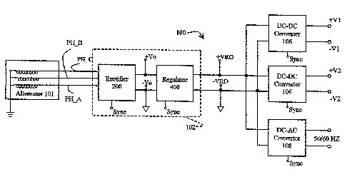
[00042] Refernng now to Fig. 1, a system 100 for converting between mechanical
and
electrical energy in accordance with various aspects of the present invention
comprises: an
alternator 101, a rectification and regulation system 102 (suitably comprising
a rectifier 200 and
regulator 400), one or more DC-DC converters 106, and, suitably, a DC-AC
inverter 108.
CA 02528145 2005-12-02
WO 2004/109892 PCT/US2004/017571
[00043] In general, alternator 101 provides multi-phase (e.g. three-phase)
unregulated AC
output signals, phase A (PH A), phase B (PH B), and phase C (PH C) that vary
significantly in
accordance with drive RPM. Rectification and regulation system 102 rectifies
the AC output
signal from alternator 101, i.e. converts it into a DC signal (VRO), and
regulates the voltage of
that signal at a predetermined level, e.g. 180V, i.e., maintains the voltage
level with a tolerance
of ~ 2 %. The regulated DC signal (VRO) is then applied to DC-DC converters
106 for
conversion to a desired output voltage levels) (V1, V2), e.g., 12, 24 and/or
42 volts DC and, if
desired, to DC-AC inverter 108 which generates an AC signal of desired
waveform, frequency,
and voltage, e.g. 50!60 Hz, 120 V RMS sine wave. The predetermined voltage
level VRO, e.g.
180V, output by rectification and regulation system 102 is chosen to support
the desired outputs.
In the preferred embodiment, the output VRO of rectification and regulation
system 102 is
chosen to be approximately 180V, which, when applied to DC to AC inverter 108
produces a
170 V peak, that is, 120V RMS sine wave. The same regulated 180V DC signal VRO
is fed to
DC-to-DC step down converters) 106 for producing 12, 24 and/or 42V DC outputs.
Since VRO
is relatively high, relatively low levels of current flows into the input
section of DC-to-DC
converters 106, yielding higher power conversion efficiency.
[00044] Use of rectification and regulation system 102 to rectify and regulate
the output
voltage of the alternator at a relatively high voltage, and then using one or
more separate DC to
DC converters andlor DC to AC inverter to convert the initial relatively high
voltage to the
desired output voltage is particularly advantageous in a number of respects.
Rectification and
regulation at relatively high voltages equates to use of relatively low
current levels, as compared
to the magnitude of current encountered if rectification and regulation were
performed at lower
voltages. The use of lower magnitude current reduces both conduction and
switching losses in
connection with the rectification and regulation functions. Thus, less heat is
generated. Further,
performing all rectification and regulation separately from the conversion
function permits use of
less expensive, more rugged and simpler voltage output stages, and facilitates
generation of
multiple voltage outputs, e.g., 12, 24 or 42 V DC, and 120 volts RMS 50/60 Hz
AC.
[00045] Alternator 101 is suitably a permanent magnet alternator, and
preferably an
alternator of the type described in commonly owned co-pending U.S. Provisional
Patent
Application No. 601486,831 by Charles Y. LaFontaine and Harold C. Scott,
entitled "Compact
CA 02528145 2005-12-02
WO 2004/109892 PCT/US2004/017571
High Power Alternator" and filed on July 10, 2003. The aforementioned
LaFontaine et al
application serial number 60/486,831 is hereby incorporated by reference as if
set forth verbatim
herein.
[00046] Briefly, alternator 101 comprises a rotor mounted on a rotating shaft
and disposed
concentrically relative to a stationary stator. The stator includes respective
phase windings, A, B
and C connected together at one end (neutral), in a star configuration. The
winding neutral
defines a second floating ground (designated by respective vertically spaced
horizontal lines of
varying lengths forming a triangle and not to be confused with a first ground
symbolized by a
closed triangle). An external energy source, such as a motor or turbine,
commonly drives the
rotating element, directly or through an intermediate system such as a pulley
belt. In automotive
applications, alternator 101 is typically mounted under hood, and belt driven
from the vehicle
engine. Relative motion between rotor and stator causes voltage to be induced
in the windings.
Alternator 101 is preferably designed such that it generates a predetermined
minimum voltage at
idle or a minimum RPM under full load conditions. As noted above, in
automotive applications,
drive RPM can vary widely, e.g. frorn 600 RPM at idle, to 3000 RPM for large
diesel trucks,
(5:1 variation), 600 to 4,000 RPM for light duty diesels, and from 600 to 6500
RPM gasoline
vehicle engines. In addition, the alternator must accommodate variations in
load, i.e., no load to
full load. Thus the output voltage of a permanent magnet alternator101 when
used with a
gasoline vehicle engine can be subject to a 12:1 variation. Accordingly, if a
conventional
permanent magnet alternator is required to provide operating voltage (e.g. 18
volts) while at idle
speeds with a given load, it will provide multiples of the operating voltage,
e.g., ten (10) times
that voltage, at full engine RPM with that load, e.g., 180 volts.
[00047] Rectification and regulation circuit 102 rectifies the AC output
signal from
alternator 101, i.e., converts it into a DC signal, and regulates the voltage
of that signal, i.e.,
maintains the voltage level of the signal within a predetermined range of
values, e.g. 180V ~ 2
%. Rectification and regulation system 102 can comprise any system capable of
providing a
suitably regulated DC signal (VO) over the range of three-phase AC signals
provided by
alternator i O1. For example, system 102 can comprise a SCR bridge with phase
angle control of
duty cycle (and suitably employing switching loss control as will be
described). However,
system 102 preferably comprises a rectifier/limiter 200, cooperating with a
regulator 400,
CA 02528145 2005-12-02
WO 2004/109892 PCT/US2004/017571
preferably a boost type regulator. Rectifier/limiter 200 can comprise any
circuit capable of
rectifying the widely varying output of alternator 101, and limiting its
output to a predetermined
value, reducing the range of variation in the input signal VO to regulator 400
(as compared to the
alternator output). For example, rectifier/limiter 200 can be implemented by
an SCR bridge such
as described above. However, the preferred embodiment employs a multimode
rectifier/limiter
200 which selectively operates in full wave rectification, full duty cycle
half wave rectification,
or pulse width modulated half wave rectification modes depending upon
alternator output and/or
the output of the rectifier/limiter, and limits its output to a predetermined
value slightly below the
predetermined output value of system 102, e.g. 170 V. In some instances it may
be desirable to
include what is, in effect, an transitional mode of operation between full
wave rectification and
half wave rectification wherein the system dithers between full wave and half
wave rectification
modes. More specifically, within certain ranges of RPM, under certain load
conditions, full
wave rectification may generate output levels in excess of that desired.
However, half wave
rectification in. such circumstances may not provide sufficient power output.
To accommodate
those cases, when certain RPM and load conditions are encountered, dithering
between half
wave rectification and full wave rectification is effected, such that the out
voltage. (and output
power) of circuit 200 is effectively the time average of the parameter in the
two modes. The
relative time periods of half wave rectification and full wave rectification
determines the desired
output. A preferred embodiment of rectifier/limiter 200 is shown in Figure 2.
Preferred
embodiments of the respective components of such a rectifier/limiter 200 are
shown in Figure 3.
[00048] Regulator 400, receptive of the output of rectifier/limiter 200,
provides constant
voltage output VRO at a predetermined level, e.g. 180V ~ 2 %. Regulator 400 is
preferably a
boost type regulator. Use of a boost type regulator is advantageous in a
number of respects. It is
particularly simple (avoiding the necessity of a transformer), efficient, and
scalable. When the
input to regulator 400 approaches the predetermined maximum (e.g. at RPM
corresponding to
highway speeds), the boost is essentially inactive, consuming little energy,
and generating little
heat. Further, a boost type topology inherently limits the current in the
event of a short circuit. A
preferred embodiment of a boost type regulator 400 is shown in Figure 4.
Preferred embodiments
of the respective components of such a boost type regulator 400 are shown in
Figure 5.
11
CA 02528145 2005-12-02
WO 2004/109892 PCT/US2004/017571
[00049] DC - DC converters 106 derive the desired level output voltage(s),
e.g. 12, 24, or
42 volts or other desirable DC voltage, from the relatively high voltage
output of rectification
and regulation system 102 (e.g. regulator 400). DC-DC converters 106 can be
implemented
using any suitable topology, such as, for example, half bridge, full bridge in
the switch mode,
push pull, fly back, forward converter, or back boost converter. DC-DC
converter 106 is
implemented utilizing a conventional full bridge, pulse width modulated,
stepped down,
topology. A preferred embodiment of a DC-DC converter 106 is shown in Figure
6. Preferred
embodiments of the respective components of such a boost type regulator 400
are shown in
Figure 7.
[00050] DC-AC inverter 108 produces an AC output signal of the desired voltage
and
waveform, e.g.,120 volts RMS 50/60 Hz AC, from the output of rectification and
regulation
system 102 (e.g. regulator 400). In general a suitable inverter bridge
comprises respective pairs
of "high side" and "lower side" switching devices. One pair is associated with
the positive half
of the AC cycle, and the other associated with a negative half of the AC
cycle. The switching
devices of each pair are connected in series with a suitable output filter,
between a regulated DC
rail, i.e., the output of rectifier and regulator system 102, and common
ground, the high side
switch is connected between positive rail and output filter, and the low side
switch connected
between output filter and common ground. For ease of reference, the pair of
switches associated
with the instantaneous half cycle will hereinafter sometimes the referred to
as the "primary"
switches, and the pair of switches associated with the other half cycle
sometimes hereinafter
referred to as the "complementary" switches. In general, an AC signal is
generated by cyclically
rendering conductive, on a mutually exclusive basis, a first pair of switching
devices (e.g. the
switches associated with the positive half cycle), then the second pair of
switching devices (e.g.
switches associated with the negative half cycle), for periods corresponding
to one half cycle
(180°) of the desired frequency. This generates an essentially square
wave shape, which is
smoothed by the output filter. Conventionally, wave shaping to better
approximate a sine wave is
effected by pulse width modulating the current through the primary switches.
In some instances,
wave shaping can be further facilitated by providing a discharge path for the
output filter through
at least one of the complementary switches during at least a portion of the
"dead time" between
pulses through the primary switches.
12
CA 02528145 2005-12-02
WO 2004/109892 PCT/US2004/017571
[00051 ] In the preferred embodiment, inverter 108 produces an output signal
having a
predetermined frequency and wave shape, e.g. 60 hertz sine wave, by
maintaining the high side
switch of the pair associated with the instantaneous half of the AC cycle "on"
for the entire half
cycle and modulating the lower (ground side) switch, (as opposed to modulating
both switches of
the pair), and, when the load (current draw) is below a predetermined level
(but not when the
load reaches or exceeds that level), turning on the high side of the
complementary pair
(associated with the other half cycle) in a mutually exclusive fashion with
low side of the
primary switches) to make sure that the inverter filter inductor and the
capacitor are reset. Such
a preferred inverter 108 is shown in Figure 8, and with waveforms in Figure 9.
Preferred
embodiments of the respective components of such an inverter 108 are shown in
Figure 10.
[00052] As will be further discussed, provisions are preferably made within
rectifier/limiter 200, regulator 400, DC-DC converter 106 and inverter 108 to
limit the rate of
change of the voltage across, and current through, power switches employed in
the system to
minimize the switching energy that would otherwise be dissipated as heat, and,
preferably,
recapture that switching energy and direct it to the load.
Rectifier/Limiter 200
[00053] As previously noted, rectifier/limiter 200 can comprise any circuit
capable of
rectifying the widely varying output of alternator 101, and limiting its
output to a predetermined
value. Preferably, however, rectifier/limiter 200 comprises a mufti-mode
circuit which
selectively operates in full wave rectification, full duty cycle half wave
rectification, transitional
dithering between full wave and full duty cycle half wave rectification, or
pulse width modulated
half wave rectification modes depending upon alternator output and/or the
output of
rectifier/limiter 200. In general, full wave rectification is most efficient,
and, accordingly, it is
desirable to operate in that mode, except when full wave rectification would
generate a voltage in
excess of the predetermined maximum output level, e.g. 170 volts. As will be
explained, the
points at which the operational mode is switched between full wave
rectification and half wave
rectification can be determined based upon an indicia signal (V SNS)
representative of the
output that would be produced by full wave rectification under instantaneous
RPM and load
conditions irrespective of the actual rectification mode. Indicia signal V
SNS, as will be
13
CA 02528145 2005-12-02
WO 2004/109892 PCT/US2004/017571
explained, is suitably directly proportional to the output voltage level that
would be generated by
full wave rectification of the alternator output under instantaneous RPM and
load conditions
(irrespective of the actual rectification mode) except that increased IR drop
experienced in
alternator 101 during half wave rectification mode operation is reflected as a
decreased voltage
in the indicia signal. The point at which pulse width modulation of the half
wave rectifier signal
is initiated is determined by monitoring the rectifier/limiter output.
[00054] Rectifier/limiter 200, upon startup, initially operates in the full
wave rectification
mode. When rectifier/limiter 200 is in the full wave rectification mode a
switch to half wave
rectification is made when indicia signal V SNS exceeds a predetermined level
(FULL UPPER LIMIT) corresponding to the maximum desired output of
rectifier/limiter 200 to
maintain the output of rectifier/limiter 200 below the maximum level. When
rectifier/lixniter 200
is in the half wave rectification mode a switch to full wave rectification is
made when indicia
signal V SNS _drops below a predetermined lower threshold level (HALF LOWER
LIMIT)
corresponding to a voltage equal to or, preferably, slightly less than the
maximum desired output
of rectifier/limiter 200, and indicating that full wave rectification will
once again produce an
output within the desired limits. On the other hand, if rectifier/limiter 200
is in the half wave
rectification mode, and the output of rectifier/limiter 200 reaches the
maximum desired output
level, pulse width modulation is initiated to prevent the maximum level from
being exceeded.
Dithering occurs when a transition is made between full wave rectification and
half wave
rectification modes, and either half wave rectification results in a value of
indicia signal V SNS
less than HALF LOWER LIMIT, or full wave rectification results in a value of
indicia signal
V SNS greater than FULL UPPER LIMIT. During a dithering operation, the output
of
rectifier/limiter 200 is, effectively, the time average of the instantaneous
output of successive
cycles of full wave rectification and half wave rectification, thus providing
an output signal
within the desired limits. The band of conditions in which dithering occurs is
determined by the
difference between the upper and lower threshold values.
[00055] Alternatively, the points at which the operational mode is switched
between full
wave rectification and half wave rectification (as well as initiation of pulse
width modulation)
can be determined by monitoring the output VO of rectifier/limiter 200
Refernng briefly to
Figure 2A, rectifier/limiter 200 initially operates in the full wave
rectification mode. As RPM
14
CA 02528145 2005-12-02
WO 2004/109892 PCT/US2004/017571
increases (assuming constant load), the output voltage of rectifier/limiter
200 (e.g., generally
indicated as 260 in Figure 2A) increases proportionately. Rectifier/limiter
200 is maintained in
full wave rectification mode until, in effect, the output VO reaches a
predetermined limit
corresponding to the desired maximum output value of rectifier/limiter 200,
e.g., 170 V. The
maximum value is reached, for example, when the speed increases to
approximately a
predetermined multiple of idle RPM, e.g., 2.5 times idle speed. When (e.g.,
point 262 in Figure
2A) output VO exceeds the desired maximum level (corresponding to indicia
signal V SNS
exceeding upper threshold FULL UPPER LIMIT), rectifier/limiter 200 is switched
to half wave
rectification mode (initially with full duty cycle). Switching to half wave
rectification (full duty
cycle) effectively decreases output voltage VO by a factor of between
approximately 50% and
60% (e.g., point 264 in Figure 2A), depending upon load (current draw)
conditions (the greater
the load, the greater the drop). Assuming no dithering condition, (e.g. the
half wave rectification
output voltage VO, when first switched, is greater than a lower threshold
level corresponding to
HALF LOWER LIMIT), as RPM continues to increase rectifier/limiter 200 will
continue to
operate in the full duty cycle half wave rectification mode until the output
voltage of
rectifier/limiter 200 reaches a predetermined level, preferably the desired
maximum output value
(point 266 in Figure 2A), at which point pulse width modulation of the half
wave rectified output
of rectifier/limiter 200 is effected to limit the output to the predetermined
level. On the other
hand, if, when rectifier/limiter 200 is operating in the half wave
rectification mode, the RPM
decreases (or the load increases) to the point that the output VO drops below
the lower threshold
level (corresponding to HALF LOWER LIMIT), full wave rectification of
operation is
resumed.
[00056] Refernng briefly to Figure 2B, if, when a transition is made between
full wave
rectification and half wave rectification modes, either half wave
rectification results in output
VO dropping below the lower threshold level (corresponding to HALF LOWER
LIMIT) (point
265 in Figure 2B), or full wave rectification results in an output VO higher
than the desired
maximum level (corresponding to FULL UPPER LIMIT) (e.g., point 270 in Figure
2B),
rectifier/lirniter 200 suitably operates in the dithering mode, switching
between full wave and
half wave rectification such that the time averaged output of
rectifier/limiter 200 is within the
desired limits. Rectifier/limiter 200 typically continues to operate in the
dithering mode until the
RPM increases (or load decreases) to a point where the half wave rectification
mode operation
CA 02528145 2005-12-02
WO 2004/109892 PCT/US2004/017571
generates a voltage in excess of the lower threshold level (corresponding to
HALF LOWER LIMIT) (e.g., point 272 in Figure 2B) or the RPM decreases (or load
increases)
to a point where the full wave rectification mode operation generates a
voltage less than or equal
to the desired maximum level (corresponding to FULL UPPER LIMIT).
[00057) Referring to Figure 2C, rectifier/limiter 200 preferably comprises: a
rectifier
bridge circuit 202 cooperating with suitable buffer and driver circuit 206; a
half bridge
conversion circuit 203 cooperating with a suitable comparator and PWM drive
generator 216A
and an isolation boundary (buffer) circuit 216B; a zero crossing detector
circuit 213; a
microprocessor control 214; a isolated power voltage source 215; a voltage
sense isolation circuit
217; and a low voltage power supply 218. Rectifier/limiter 200 preferably also
includes a
switching loss reduction circuit 204, and, if desired, may also include a
current sensing circuit
212.
[00058) Rectifier bridge circuit 202, when actuated in response to a control
signal
SCR DRV from microprocessor control 214 (as conditioned by buffer and driver
circuit 206),
provides full wave rectification of the three-phase AC signal from alternator
101, generating a
DC signal VO between terminal +VO and common ground (-VO). Rectifier bridge
circuit 202
suitably comprises a respective parallel leg associated with each AC phase,
each leg comprising
a serially connected "upper" diode and "lower" (ground side) power switch,
e.g. SCR, with the
associated alternator phase connected to the juncture of SCR and diode. As
will be discussed,
the SCRs are enabled during full wave rectification mode operation, and
disabled during half
wave rectification mode operation (both full duty cycle and PWM). A preferred
embodiment of
rectifier bridge circuit 202 is shown in Figure 3A.
[00059) Buffer and driver circuit 206 receives the SCR DRV control signal from
microprocessor control 214, and responsively generates drive signals suitable
for application to
the components (e.g. SCRs) of rectifier bridge circuit 202. A preferred
embodiment of buffer
and driver circuit 206 is shown in Figure 3B.
[00060) Half bridge conversion circuit 203, when actuated, effectively
converts rectifier
bridge circuit 212 into a half wave rectifier, by disabling the SCRs and
selectively connecting the
negative output terminal (-VO) of circuit 200, i.e., common ground, to the
neutral of the
16
CA 02528145 2005-12-02
WO 2004/109892 PCT/US2004/017571
alternator three-phase windings, i.e., the second floating ground. Half bridge
conversion circuit
203 suitably comprises one or more diodes 220 and power switches 222, such as
FETs,
cooperating with comparator and PWM drive generator 216A, and isolated driver
216B. Diodes
220 and power switches 222 provide a selective connection between negative
output terminal -
VO of circuit 200 and the neutral of alternator 101 windings. When negative
output VO of
circuit 200 (common ground) is connected to the neutral of alternator 101
windings (second
floating ground), current flows only during the positive half of the
alternator AC cycle. A
preferred embodiment of half bridge conversion circuit 203 (and driver 216B)
is shown in Figure
3C.
[00061 ] Comparator and PWM drive generator 216A, when enabled by control
signal
FET ENB from microprocessor control 214 (mutually exclusive with SCR DRV),
cooperates
with isolation boundary (buffer) circuit 216B to provide suitable drive
signals to power switches
222, and selectively effects pulse width modulation of output voltage VO to
limit the voltage to
the predetermined maximum output level (e.g., 170 volts). More specifically,
comparator and
PWM drive generator 216A, when activated by a control signal FET ENB from
microprocessor
controller 214, monitors the output voltage VO of rectifier/limiter 200 and
generates a pulse
width modulated control signal FET DRV for effecting control of half bridge
conversion circuit
203 in accordance with the output voltage VO of rectifier/limiter 200. The
duty cycle of pulse
width modulated control signal FET DRV is controlled in accordance with, e.g.,
is inversely
proportional to the output of rectifier/limiter 200; the duty cycle is
initially 100% and remains at
that value until the half wave rectification mode output of rectifier/limiter
200 exceeds the
predetermined maximum value, e.g., 170 volts, whereupon the duty cycle is
adjusted to limit the
output to the predetermined value. A preferred embodiment of PWM drive
generator 216A is
shown in Figure 3D.
[00062] Isolation boundary (buffer driver) circuit 216B, in response to the
FET DRV
signal, generates a signal of appropriate voltage and isolation (reference
ground) to drive the
FETs in the half wave rectifier. Aa noted above a preferred embodiment of
isolation boundary
circuit 216B is shown in Figure 3C.
17
CA 02528145 2005-12-02
WO 2004/109892 PCT/US2004/017571
[00063] Isolated voltage source 215, receptive of the respective phases from
alternator
101, provides an isolated, unregulated full wave rectified DC voltage PS at an
output terminal
+PS relative to a first floating ground (designated by a horizontal line
with.spaced angled lines
extending downwardly therefrom) which is isolated from the second floating
ground and the
common ground. Isolated voltage source 215 suitably comprises a conventional
diode rectifier
full bridge. Voltage PS is directly proportional to the output voltage level
that would be
generated by full wave rectification of the alternator output under
instantaneous RPM and load
conditions (irrespective of the actual rectification mode), except that
increased 1R drop
experienced in alternator 101 during half wave rectification mode operation is
reflected as a
decrease in voltage PS. A preferred embodiment of isolated voltage source 215
is shown in
Figure 3E. Isolated output voltage PS is applied to voltage sense isolation
circuit 217 and to low
voltage power supply circuit 218.
[00064] Voltage sense isolation circuit 217, cooperating with isolated voltage
source 215,
derives indicia signal V SNS indicative of voltage PS (and hence output
voltage level that would
be generated by full wave rectification of the alternator output under
instantaneous RPM and
load conditions), but conditioned and level shifted to be suitable for
application as an input signal
to microprocessor 214. A preferred embodiment of voltage sense isolation
circuit 217 is shown
in Figure 3F.
[00065] Low voltage power supply circuit 218 provides multiple isolated low
voltage
supplies for powering the various control components of system of 102,
preferably, deriving
such signals from unregulated voltage +PS. Circuit 218 preferably generates
respective
regulated signals at a predetermined voltage, e.g. 15 volts, relative to each
of common, and first
and second floating grounds. A preferred embodiment of low voltage power
supply circuit 218
is shown in Figure 3G.
[00066] Zero crossing detector 213, receptive of one of the alternator phases
e.g. phase A
(PH A), generates an output signal (ZC) indicative of zero crossings of the
phase, and hence
RPM. Zero crossing signal ZC is applied as an input to microprocessor
controller 214. A
preferred embodiment of zero crossing detector 213 is shown in Figure 3H.
18
CA 02528145 2005-12-02
WO 2004/109892 PCT/US2004/017571
[00067] Current sensing circuit 212 generates a current sense signal, I SNS,
indicative of
the magnitude of current being put out by alternator 101. Current sense signal
I SNS is applied
as an analog input to microprocessor 214. A preferred embodiment of current
sensing circuit 212
is shown in Figure 3I.
[00068] Microprocessor controller 214, responsive to full wave output indicia
signal
V SNS, zero crossing signal ZC and, if desired, current sense signal I SNS,
selectively
generates control signals: SCR DRV to effect full wave rectification mode
operation; and
FET ENB to effect half wave rectification mode. Prior to entering the
multirnode operation of
system 102, an initial determination that the engine driving alternator 101 is
running on its own
power, as opposed to, e.g., being cranked by a starter motor can be provided.
In essence, RPM
as reflected by the period between zero crossings in one of the alternator
phases is monitored to
ensure that the motor is operating at idle speed or above for a predetermined
period before
initiating the multimode operation.
[00069] A preferred embodiment of microprocessor controller 214 is shown in
Figure 3J.
Controller 214 suitably comprises Microchip PIC18242 microcontroller
configured to include:
[00070] Tirner 0 (TMRO) configured as an 8-bit counter driven by an internal
clock.
The timer value is reloaded on each rollover to create an interrupt event from
timer 0 at a fixed
time base, e.g.,100 us.
[00071] Timer 1 (Ml) configured as a 16-bit counter driven by an internal
clock.
The timer value is used to measure the period of successive zero-crossings
from the alternator.
An interrupt from Timer 1 indicates a rollover, signifying that the time
between successive zero-
crossings are too long and RPM is too low.
[00072] External Interrupt 0 (INTO is the event name) An interrupt is
triggered
when the INTO pin (receptive of zero crossing signal ZC from zero crossing
detector 213) goes
high.
[00073] File (RAM) pointer: A 12 bit pointer for access of the file (RAM)
space data.
This hardware pointer is used to clear RAM and to store history in the analog
thread.
19
CA 02528145 2005-12-02
WO 2004/109892 PCT/US2004/017571
[00074] Analog-to-Digital converter: This hardware module reads from the
selected input
channel (V SNS, I SNS) and stores an 8-bit or 10-bit result. The channel
selected is controlled
by a control register ADCONO bits 5, 4 & 3.
[00075] 3 Input/output ports: Two 8-bit ports (PORTB and PORTC) for digital
only and
a 6-bit port (PORTA) that can be digital or analog or a mixture of both. Each
bit within a port.
can be configured as a digital input or output. The 6-bit port (PORTA) can
also be configured to
receive an analog input. In this case, digital outputs SCR DRV and FET ENB are
generated at
port B bits RB6 and RB7.
[00076] A flowchart of the program executed by microprocessor 214 is provided
in
Figures l0A-K. In general, the program is composed of normal initialization,
start-up and "main
loop" sequences. .
[00077] Prior to entering the multimode operation of system 102, an initial
determination
that the engine driving alternator 101 is running on its own power, as opposed
to, e.g., being
cranked by a starter motor can be provided.
[00078] The "start-up" sequence is employed to ensure that the engine driving
alternator
101 is up to speed and running on its own power before the system begins to
draw power. It is
not desirable to draw power from an engine that is attempting to start.
Accordingly, after a
conventional initialization sequence, the "start-up" sequence, in effect,
detects a predetermined
period of normal speed operation (a predetermined number of consecutive
measurements of zero
crossing periods below a specified number) before advancing to the main
sequence. If a period
larger than the specified number is detected, the count is started over.
Accordingly, an engine
coming up to speed and then faltering will not trigger a draw of power. After
it is determined that
the engine is "up-to-speed." the SCR DRV signal is generated (SCR DRV = l and
FET ENB =
0) to enable full bridge 202 and effect initial full wave rectification.
[00079] The main loop sequence is then initiated. The main loop monitors the
voltage
indicia signal (V SNS), and selectively generates control signals SCR DRV and
FET ENB to
switch between full wave and half wave rectification modes. When switching
between modes, a
"break before make" is employed to avoid shorting the alternator windings.
This function is
CA 02528145 2005-12-02
WO 2004/109892 PCT/US2004/017571
suitably implemented as a "thread". A thread is made up of respective small
pieces of code (a
state) that each perform a task and then return. Linked sequencing is provided
through
determining in each state which state will be the next to execute when the
thread is called again.
In general a thread must be called several times in order to complete the over-
all function. The
main loop comprises three primary calls:
[00080] GetAnaloglnputs: acquires analog inputs (V_SNS, I SNS), stores each
result in a
buffer and calculates the average of each buffer. The analog inputs are
monitored every time
base (100 us). Upon completion of the process, a flag is set.
[00081] BridgeControl: Checks for the flag indicating that the analog channels
have been
read, buffered and the averages calculated, then determines if a change in the
bridge mode is
required based upon the readings. If the current mode is full wave
rectification, V SNS is tested
for greater than the upper limit (FULL UPPER LIMIT). If the current mode is
half wave
rectification, V SNS is tested for less than the lower limit (HALF LOWER
LIMIT). If a change
is indicated, the sequence to change the bridge mode is initiated and control
is returned to the
thread loop. Subsequent calls to the thread continue to wait for delays or
finish the mode change
if the delay is complete.
[00082] UpdatePeriodBuffer: check flag for a new zero-crossing measurement.
Test
another flag to see if the period was "too low", if so, just return and do
nothing with that reading.
Place the new period in a circular buffer. Calculate the average of the buffer
and store the result
in'avg~eriod'.
[00083] In addition, several "support" functions are employed:
InitCpuRam: Initializes control registers and clears all used RAM
InitSpecialVals: Sets up variables or registers specific to this program
WriteHistory: Used by the analog thread to store an analog result in the
proper position
within the analog history array.
CaIcADHistAvg: Used by the analog thread to calculate the average of a section
of the
analog history array used for a single channel.
21
CA 02528145 2005-12-02
WO 2004/109892 PCT/US2004/017571
Switching Loss Reduction Circuit 204
[00084] ~ In high power applications employing power switches such as half
bridge
conversion circuit 203, switching losses, i.e. IR loss occurring during
switching operations, can
be a serious problem. As a rule of thumb, in the absence of special
provisions, approximately
10% of the input electrical energy may be lost in the form of heat. Therefore,
for a 10 kW power
conversion, 1 kW of energy may be lost in the form of heat. Such heat can have
deleterious
effects, e.g. reduced reliability, on not only the power switches, but also
other electronic
components of the system. In addition, during transitions, the rapid change in
voltage across
and/or current through switching devices tends to create radio frequency
emissions, i.e.
interference.
[00085] In general, a power switching device, such as an FET, requires a
finite amount of
time, e.g., 500 nanoseconds, (referred to herein as a "turn-off period") to
change from a fully
conductive "on" state (in which the resistance of the device is negligible) to
a fully non-
conductive "off' state (in which the resistance of the device is effectively
infinite). During this
turn-off period the resistance of the device changes gradually from negligible
to effectively
infinite. Until the resistance reaches a sufficient level, current continues
to flow through the
device, causing IR loss.
[00086] In general, the resistance exhibited by an FET power switch is a
function of the
voltage level of the drive signal applied to its gate. For example, referring
to Figures 3L and 3M,
such a device is rendered "on", i.e., fully conductive (e.g., R = ~0) by drive
signals at or above a
predetermined voltage, e.g. 15 volts, and "off', i.e. fully nonconductive
(resistance is effectively
infinite, e.g. R = ~4M Sl or more.) by drive signals at or below a second
predetermined voltage,
e.g. zero volts. When "on," the device conducts at a relatively high level,
e.g. 100 A. However,
the resistance of the device is negligible, so the voltage drop across the
device is essentially zero.
When the device is "off', a relatively high level of voltage appears across
the device. However,
since practically no current flows through the device there is essentially no
IR loss.
[00087] On the other hand, significant IR loss can occur when drive signals of
intermediate voltages are applied, the device is conductive but manifests an
intermediate
resistance. For example, the resistance of the switch is a first intermediate
value on the order of
22
CA 02528145 2005-12-02
WO 2004/109892 PCT/US2004/017571
ohms, and a second greater value, on the order of kilo-ohms, in response to
drive signals of 7
volts, and 4 volts, respectively. This tends to result in significant IR loss.
For example, under
typical operating conditions, when the device resistance is in the kilo ohm
range, e.g., the drive is
in the vicinity of 4 volts, significant levels of current, e.g. on the order
of 50 A, flow through the
device. This equates to significant IR loss, e.g. 2.5 kW during that period.
This becomes
particularly significant when the switching device is turned on and off at
relatively high
frequencies, e.g., in pulse width modulation operation. From the perspective
of minimizing IR
loss, it is therefore desirable to minimize the turn-off period. The minimum
turn-off period,
however, tends to be established by the gate capacitance of the FET, and for
high power rated,
low on-resistance devices may be on the order of hundreds (e.g., 500) of
nanoseconds.
[00088] In accordance with one aspect of the present invention, conversion
efficiency is
increased, and electromagnetic emissions (interference) reduced, by
controlling the rate of
change of voltage across and current through the power switching device during
the switch turn-
off period, minimizing energy generated during the course of turning off the
power switch that
would otherwise be dissipated in the power switches as heat. The energy is
preferably captured
and ultimately applied to the load by, e.g., feeding it forward to the load,
or feeding back to a
voltage source. This can be accomplished by disposing a capacitor across the
power switch such
that it is charged during the turn-off period, limiting the rate of change of
voltage across the
switch, then selectively discharging the capacitor non-dissipatively
(preferably for ultimate
application to the output) to a substantially fully discharged state by the
beginning of the next
successive turn-off period. The turn-off period is of finite duration, e.g.,
500 ns. Thus, by
limiting the rate of change of voltage, the voltage developed across the FET
during the turnoff
period is limited to a relatively low predetermined level. Substantially
reducing switching loss
has three primary benefits: higher power conversion efficiency; reduced heat
dissipation in the
power switch (and thus higher reliability); and reduced electro-magnetic
interference.
[00089] More specifically, a capacitor opposes changes in voltage, and charges
only
gradually. The change in voltage (~V) across the capacitor, over a period of
time (fit) is in
accordance with the capacitance (C) and the average value of the current (i)
during the time
period, i.e., OV=[(i x ~t)/C)]. Thus, by disposing an appropriate value of
capacitance across the
drain and source of the FET, the voltage that develops between the drain and
source of the FET
23
CA 02528145 2005-12-02
WO 2004/109892 PCT/US2004/017571
during the FET turn-off period can be kept at low value. The higher the value
of the capacitor,
the lower the voltage that develops between the drain and the source during
the turn-off period.
(However, the capacitance is preferably not so large that it cannot be
discharged between
successive turn-off periods.) 'In general, the value of the capacitance is
chosen such that the
voltage developed during the turn-off period is less than a predetermined
value, suitably less than
20 volts, and preferably 10 volts or less. In the preferred embodiment, the
voltage developed
during the turn-off period is limited to 10 volts. The value of capacitance
(CS) to limit the
voltage between the drain and source of the FET to a predetermined value (Vas)
during the turn-
off period is equal to the average current (lave) through the FET multiplied
by the duration (Tuff)
of the turn-off period divided by the predetermined voltage (Vas), i.e., CS =
[(Ia~e x To~)/Vas]. In
the preferred embodiment, typical values of such capacitor range between 0.1
microfarad to 0.2
microfarad. After the FET is completely turned off, or during the next
successive period when
the FET is turned on, the energy captured by the capacitor, i.e. the charge
developed on the
capacitor during the turn-off period, is discharged into an inductor which non-
dissipatively
discharges the capacitor) and ultimately applies the energy to the output (fed
forward) or is fed
back to the input power source to effectively recycle the energy with out
direct dissipation. In
the preferred embodiment, the power source voltage and FET switching times
result in capacitor
values that are discharged within the time allotted by inductance values of
about 53 ~.H.
[00090] Referring again to Figure 2C, in the preferred embodiment control of
the rate of
change of voltage across and current through power switching device 222 during
the turn-off
period is effected switching loss reduction circuit 204. Circuit 204 suitably
comprises a diode
240, a capacitor 242, an inductor 244, and a switching device 246, e.g., a
FET, cooperating with
a suitable driver circuit 24?, and a diode 248. Diode 240 and capacitor 242
are connected across
switching device 222 (e.g., for a FET switch, the anode of diode 240 is
connected to the drain of
the FET and capacitor 242 is placed between the cathode of the diode and the
FET source).
Switching device 246 is connected in series with inductor 244 across capacitor
242. Diode 248 is
disposed to provide a directional current path between inductor 244 and output
terminal +VO.
Switching device 246 suitably operates in synchronism with power switch 222.
When switches
246 and 222 are on, capacitor 242 discharges into inductor 244. When switches
246 and 222 are
off, two things happen, essentially simultaneously: capacitor 242 charges,
controlling the voltage
24
CA 02528145 2005-12-02
WO 2004/109892 PCT/US2004/017571
across switch 222 as previously described, and inductor 244 effectively
reverses its polarity,
thereby forward-biasing diode 248 and delivering current through diode 248 to
terminal +VO. A
preferred embodiment of switching loss reduction circuit 204, is shown in
Figure 3K.
[00091] Analogous switching loss reduction circuits are suitably employed with
the power
switches of regulator 400, DC-DC converter 106 and inverter 108.
Regulator 400
[00092] As previously noted, regulator 400 provides a constant voltage at a
predetermined
level, e.g. 180V + 2 %. Referring to Figure 4, regulator 400 is preferably a
boost type regulator
comprising one or more boost stages 404, a control circuit 412, and,
preferably, a switching
energy loss reduction circuit 410 (analogous to circuit 204 in
rectifier/limiter system 200). Boost
stage 404 suitably includes an input capacitor 420, an inductance 422, a boost
diode 424, a
power switch 426 and associated driver circuitry 428 (responsive to control
signals from control
circuit 412), and an output storage capacitor 432. The output is provided
across output terminals
+VRO and VRO (common ground).
[00093] The input DC voltage VO from rectifier/limiter 200 is limited to a
value, e.g. 170
volts, lower than the desired voltage at the output VRO of regulator 400,
e.g., 180 V. When
power switch 426 is turned on (in response to control signal DRV from control
412), it
completes a current path through inductor 422, causing inductor 422.to
energize. Boost diode
424 is reverse-biased. When power switch 426 turns off, inductor 422
effectively reverses its
polarity, thereby forward-biasing diode 424. Inductor 422 delivers current
through diode 424 to
charge storage capacitor 432. The voltage across inductor 422 adds to the
input voltage VO to
generate the output voltage VRO.
[00094] Control circuit 412 regulates output voltage VRO by sensing the output
voltage,
comparing it to a reference value, and varying the turn on and off time of
power switch 426
accordingly, i.e., pulse width modulates the drive to switch 426. As input
voltage (VO from
rectifier/limiter 200) to the boost regulator 400 increases, control circuit
412 decreases the
amount of time the power switch 426 is on. When the input voltage VO from
rectifier/limiter
200 is at its maximum limit, e.g. 170 volts, the power switch remains off and
essentially all of
CA 02528145 2005-12-02
WO 2004/109892 PCT/US2004/017571
the power flows through the diode 424. This results in particularly high power
throughput
efficiency; the only heat generated is that dissipated by diode 424. In
addition, boost regulator
400 inherently limits the current in the event of a short-circuit.
[00095] In addition, conversion efficiency can be increased, and
electromagnetic
emissions (interference) reduced, by inclusion of switching loss reduction
circuit 410 (analogous
to circuit 204 in rectifier/limiter 200) to control the rate of change voltage
across and current
through switching device 426 during turn-off periods, minimizing energy
generated during the
course of fuming off power switches that would otherwise be dissipated as heat
and preferably
recapturing and directing it (ultimately) to the load by, e.g., feeding it
forward to the load.
Circuit 410 suitably comprises a diode 450, a capacitor 452, an inductor 454,
a switching device
456 e.g. a FET, cooperating with a suitable driver circuit 458 and a diode
460. Diode 450 and
capacitor 452 are connected across switching device 426 (e.g., for a FET
switch, the anode of
diode 450 is connected to the drain of the FET and capacitor 452 is placed
between the cathode
of the diode and the FET source). Switching device 456 is connected in series
with inductor 454
across capacitor 452. Diode 460 is disposed to provide a directional current
path between
inductor 454 and output terminal +VRO. Switching device 456 suitably operates
in synchronism
with power switch 426. When switches 426 and 456 are on,~ capacitor 452
discharges into
inductor 454. When switches 426 and 456 axe off, capacitor 452 charges
(controlling the voltage
across switch 426 as previously described in conjunction with circuit 204),
and inductor 454
effectively reverses its polarity, thereby forward-biasing diode 460 and
delivers current through
diode 460 to terminal +VRO.
[00096] A preferred embodiment of regulator 400 suitably employs a plurality
of boost
stages 404, with each stage including respective pairs of inductors and
switches, each pair
operating periodically (e.g., 50% duty cycle) on a mutually exclusive basis.
Each pair would
have a respective diode 450 associated therewith, and preferably a portion of
capacitor 452
(parallel components being utilized to form capacitor 452). Preferred
embodiments of the
components of regulator 400 are shown in Figure 5: a boost stage 404 (and
associated elements
of switching loss reduction circuit 410) in Figure SA; switching loss
reduction circuit 410 in
Figure SB (elements common to all stages); and control circuit 412 in Figure
SC.
26
CA 02528145 2005-12-02
WO 2004/109892 PCT/US2004/017571
Inverter 108
[00097] Inverter 108 may comprise any circuit capable of producing an AC
output signal
of the desired voltage and waveform, e.g., 120 volts RMS 50/60 Hz AC, from the
output of
rectification and regulation system 102 (e.g. regulator 400). Referring to
Figure 8, a suitable
inverter bridge comprises: a first "high side" (upper) switching circuit 802
(e.g. comprising one
or more FETs) (+IJ) and associated driver circuitry 804, associated with the
positive half cycle of
the inverter output; a second "high side" (upper) switching circuit 806 (-I~
and associated driver
circuitry 808, associated with the negative half cycle of the inverter output;
a first "low side"
(lower) switching circuit 810 (+L) and associated driver circuitry 812,
associated with the
positive half cycle of the inverter output; a second "low side" (lower)
switching circuit 814 (-L)
and associated driver circuitry 816, associated with the negative half cycle
of the inverter output;
suitable filter circuitry 822 typically including an inductor and a capacitor;
current sensing
circuitry 824; and a controller 826. In the preferred embodiment, inverter 108
further includes
respective switching loss reduction circuits 818 and 820 (analogous to circuit
204 in
rectifier/limiter 200), cooperating with low side switching circuits 810 and
814, respectively.
The switching devices associated with a given half cycle (802, 810; 806, 814)
are connected in
series with filter 822, between a regulated DC rail, i.e., the output VRO of
rectifier and regulator
system 102, and common ground. The high side switch (802, 806) is connected
between positive
rail +VRO and filter 822, and the low side switch (810, 814) connected between
output filter 822
and common ground. The AC output is output from filter 822. Current sensor 824
provides an
output signal I SNS indicative of the AC current. Controller 826 provides
control signals to
drivers 804, 808, 812 and 814.
[00098] Preferred embodiments of the components of inverter 108 are shown in
Figure 10:
switching circuit 802 and driver circuitry 804 in Figure 10A; switching
circuit 806 and driver
circuitry 808 in Figure 10B; switching circuit 810 and driver circuitry 812 in
Figure 10C;
switching circuit 814 and driver circuitry 816 in Figure lOD; switching loss
reduction circuits
818 and 820 in Figure 10E; filter circuitry 822 and current sensing circuitry
824 in Figure l OF;
controller 826 in Figure l OG.
27
CA 02528145 2005-12-02
WO 2004/109892 PCT/US2004/017571
[00099] In general, an AC signal is generated by cyclically rendering
conductive, on a
mutually exclusive basis, a first pair of switching devices (e.g. the switches
802, 810 associated
with the positive half cycle), then the second pair of switching devices (e.g.
switches 806, 814
associated with the negative half cycle), for periods corresponding to one
half cycle (180°) of the
desired frequency, e.g. approximately 8.33 ms for a 60 Hz signal. This
generates an essentially
square wave shape, which is smoothed by output filter 822; the wave shape,
however, often only
remotely approximates a sine wave.
[000100] One conventional method of wave shaping to better approximate a sine
wave is
pulse width modulating the drive signals to the "primary" switches (pair of
switches associated
with the instantaneous half cycle). For example, referring to Figure 9A, a
cycle of a sine wave
850 includes a positive half cycle 852 (0-180°) and negative half cycle
854 (180-360°). The time
period corresponding to each cycle is, in effect, subdivided into a
predetermined number of
nominal intervals (PWM frames) (e.g. 48 in Figure 9, for ease of illustration,
in the preferred
embodiment 1000 intervals of 16.66 ACS duration), preferably including a short
dead time at the
end of each frame. Each PWM frame corresponds to a predetermined angular
portion of the
waveform (resolution), e.g., approximately 7.5° in the illustrative
example of Figure 9 (in the
preferred embodiment 0.36°.) The primary switches (802 (+T~, 810 (+L)
for positive half cycle
852, or 806 (-L>), 814 (-L) for negative half cycle 854) are then turned on
only for a portion of
each (typically each) of the time increments. Conventionally, both the upper
and lower primary
switches are switched on and off simultaneously, as illustrated in Figure 9A.
In. either case, the
duty cycle may range from less than 1% to over 97%.
[000101] The percentage of the time increment during which the switches are
turned on
(the duty cycle) during an individual interval is varied as a function of the
desired corresponding
waveform instantaneous, relative amplitude to simulate the desired sinusoidal
waveform. In
general, however, the duty cycle of the primary switches is typically at a
minimum value during
the time period corresponding to 0°, increases gradually in successive
increments until reaching
full duty cycle at the time period corresponding to a phase of 90°,
then decreasing
(symmetrically with the first 90°) until reaching the minimum at
180°. In a simplified example of
7.5° increments (resolution), exemplary values of the duty cycle of the
primary switches during
various incremental time periods might be 5% for the time period corresponding
to a phase of 0-
28
CA 02528145 2005-12-02
WO 2004/109892 PCT/US2004/017571
7.5°, 10% for the time period corresponding to a phase of 7.5-
15°, 50% for the time period
corresponding to a phase of 36.6-44°, 100% for the time periods
corresponding to a phase of
82.5-90° and 90-97.5°, 50% for the time period corresponding to
a phase of 127.5-135°, and 5%
for the time period corresponding to a phase of 172.5-180°.
[000102] As previously noted, basic wave shaping (e.g. smoothing) is provided
by filter
822. In essence, the inductor and capacitor of filter 822 store magnetic and
electrical energy
during the period when current flows through the primary switches. However, if
the inductor
fails to completely discharge during the intervening dead time before the next
successive pulse
(that portion of the time interval during which the primary switches are
turned off), distortion of
the waveform may result. This is because any remnant energy left in the filter
will add to the
energy injected by the next pulse. The sum of these energies will not yield
the intended value.
Conventionally, to ensure that output filter 822 is completely
discharged/reset for each time
interval, a discharge path through the complementary switches is provided for
at least a portion
of the "dead time" between pulses. Conventionally, as illustrated in Fig 8A,
both the upper and
lower complementary switches (-U, -L during the positive half cycle, and +U,
+L during the
negative half cycle) are switched on and off simultaneously to provide the
discharge path. The
complementary switches are typically turned on for a period inversely
proportional to the duty
cycle of the primary switches. For example, when the duty cycle of the primary
switches is at
maximum value during an interval, the complementary switches are turned on for
a time period
corresponding to the minimum duty cycle of the primary switches.
[000103] In general, the larger the number of incremental time periods into
which the half
cycle is divided (i.e., the higher the "resolution" of the simulation), the
more closely a sinusoidal
waveform is approached. However, the greater the number of times that the
power switches are
turned off, the greater the switching loss, and concomitant heat. One way to
reduce such losses is
to employ respective switching loss~reduction circuits (analogous to circuit
204) with respect to
each of the switches in inverter bridge 604. Use of a boost-type regulator 400
facilitates
recapture of the energy collected by such circuits; the energy collected can
be fed back to the
input source without affecting regulation. If the voltage starts to increase,
the boost regulator
feedback control circuitry will compensate.
29
CA 02528145 2005-12-02
WO 2004/109892 PCT/US2004/017571
[000104] In accordance with another aspect of the present invention,
conduction and
switching losses in inverter may also (or alternatively) be reduced by, as
illustrated in Figure 9B:
(a) maintaining one of the primary switches (preferably the high side switch)
conductive during
the entire corresponding half cycle, and pulse width modulating only the other
(e.g. low side)
primary switch; and/or (b) effecting complementary pulse width modulation (i)
only of the
complementary switch corresponding to the primary switch that is held on for
the half cycle (e.g.
the high side complementary switch). Modulating only one of the primary
switches (e.g. the low
side switch), and maintaining the other primary switch on for the entire half
cycle, in effect, cuts
the number of heat generating switching transitions of the primary switches in
half as compared
to conventional techniques. Likewise, providing the complementary discharge
modulation
through only one of the complementary switches (e.g. high side switch)
similarly, in effect, cuts
the number of heat generating switching transitions of the complementary
switches in half as
compared to conventional techniques.
[000105] In addition, the present inventors have determined that with loads
above a
predetermined level (e.g. in the range of 1 KW to 2 KW), it is not necessary
to provide a specific
discharge path between pulses in. order for filter 822 to completely
discharge. Accordingly, in
accordance with yet another aspect of the present invention, the number of
switching transitions
of the complementary switches can fiirther be reduced by effecting the
complementary switch
discharge path modulation only at power levels below the threshold. At power
levels above the
threshold, the complementary switches are maintained off for the duration of
the half,cycle.
Thus, not only are switching transitions avoided, but the transitions of the
complementary
switches occur at relatively loads, so that the switching loss is at
relatively low levels.
[000106] Referring again to Figure 8, switches 802, 806, 810, and 814 are
selectively
rendered conductive by control signals from controller 826 applied to the
associated drivers 804,
808, 812 and 814.
[000107] In the preferred embodiment, controller 826 is responsive to input
signals I SNS
from current sensor 824, and Vout I and generates control signals including:
CA 02528145 2005-12-02
WO 2004/109892 PCT/US2004/017571
DLE To selectively enable positive lower drive
812 during the
positive half cycle for actuation in accordance
with a pulse
width modulated signal PWMB
DUE To selectively enable negative lower drive
816 during the
negative half cycle for actuation in accordance
with a pulse
width modulated signal PWMB.
DUT To selectively enable and actuate positive
upper drive 804
during the entire positive half cycle and,
under low load
conditions (e.g., >1KV~, in accordance with
a pulse width
modulated signal complementary (inverse) to
signal PWMB
during the negative half cycle.
DLT To selectively enable and actuate negative
upper drive 808
during the entire negative half cycle and,
under low load
conditions (e.g., >1KVV~, in accordance with
a pulse width
modulated signal complementary (inverse) to
signal PWMB
during the positive half cycle.
PWN~ Signal for effecting pulse width modulation
of the selected
lower drive 810 or 814.
SD U Tb disable negative lower drive 816 in the
event of an over
current condition.
SD L To disable positive lower drive 812 in the
event of an over
current condition.
[000108] Referring to Figure l OC, a preferred embodiment of controller 826
suitably
comprises a microcontroller 1000 with an internal PWM generator module, a
subtracting driver
1002, a conventional a half bridge driver circuit (e.g. an international
rectifier IR2111 half bridge
driver) 1004 and respective driver circuits.
31
CA 02528145 2005-12-02
WO 2004/109892 PCT/US2004/017571
[000109] As will be discussed, microcontroller 1000 generates: at pin 27
(RB6), a half
cycle period signal (POS HALF DISABLE), effectively an inverse square wave at
the desired
frequency, indicative of the instantaneous half cycle of waveform (e.g. high
during the negative
half cycle, low during the positive cycle); at pin 12 (RC1/OS1/ CCP1),
selectively, when the
output load is below the predetermined level (e.g., 1KV~, a pulse stream,
PWMC, corresponding
to the respective PWM frames (e.g. 16.66 ACS time intervals) and, at pin 13
(RC2/ CCP1), a
PWM signal with a programmed duty cycle.
[000110] The half cycle period signal (POS HALF DISABLE) is utilized to
develop high
side enable (DLT and DUT) and low side disable signals (DLE and DUE). Half
cycle period
signal (POS HALF DISABLE) is level shifted (by transistor Q14), and applied as
an input to
half bridge driver circuit 1004, which generates positive half disable (DLE)
and negative half
disable (DUE) signals, preferably including a short delay between transitions
to avoid potential
shoot through in the operation of rectifier 200, for application to low side
drivers 812 and 816
(Figure l0A). The positive half disable (DLE) and negative half disable (DUE)
signals are also
buffered by a conventional low side MOSFET driver 1006 (suitably a Micrel
MIC4424N Dual
3A-Peak low-side MOSFET driver) to derive complementary (enabling) signals DLT
and DUT,
for application to high side drivers 804 and 806 (Figure l0A).
[000111] Pulse width modulated signal PWM (pin 13) is buffered by a
conventional low
side MOSFET driver 1008 to generate a PWM drive signal PWMB, for application
to low side
drivers 812 and 816 (Figure lOA).
[000112] Pulse width modulated signal PWM (pin 13) is also applied, together
with PWM
a
frame signal PWMC (pin 12) to subtracting driver 1002. PWM frame signal PWMC
is
generated only when the output load is less than the predetermined threshold.
Subtracting driver
1002, in effect, subtracts the PWM signal from the frame signal. Subtracting
driver 1002 is thus
effectively disabled during high load periods when the frame signal is not
generated and
generates a complementary PWM signal, PWMD, when the output load is less than
the
predetermined threshold. Complementary PWM signal PWMD, is applied to both
inputs of
driver 1006, for application as a component of high side switch enabling
signals DLT and DUT.
When the inputs of driver 1006 are already at a high level by virtue of the
outputs from half
32
CA 02528145 2005-12-02
WO 2004/109892 PCT/US2004/017571
bridge driver circuit 1004, complementary PWM signal PWMD has no effect.
However, when
the output would otherwise be low, the high side enable signals track
complementary PWM
signal PWMD.
[000113] Microcontroller 1000 suitably comprises a Microchip PIC18242
microcontroller
configured to include:
Timer 0 (TMRO) Timer 0 is configured as an 8-bit counter driven by an internal
clock.
The timer value is reloaded on each rollover to create an interrupt event from
timer 0 at a
fixed time base, e.g. 100 mS.
PWM (1) is a hardware based PulseWidthModulation (PWM) module that is
controlled
by a period register PR2 and a duty-cycle that is controlled by two hardware
registers:
CCPR1L holds the upper 8 bits of the 10 bit duty-cycle, the lowest 2 bits are
held in the
control register CCP 1 CON bits 5 and 4. Once the control registers have been
written and
the.PWM module is turned on, the module will run essentially independently at
the given
period (frequency) and duty-cycle. The interrupt event from the PWM module
indicates
that a new frame has begun. This means that the value in CCPR1L was loaded
into the
module's internal registers. The CCPR1L register is a "latch" for the actual
internal duty-
cycle register, storing the contents of the internal register at the instant
of period rollover.
If the latch is not updated before the current period expires, the current
value of the latch
will be re-used.
Table pointer: A 24-bit pointer for access of the code space data. This
hardware pointer
is used for reading the duty-cycle data that is stored in the code space as a
list of
constants. The pointer is composed of three registers:
TBLPTRU: "Upper" highest 8 bits of the 24-bit pointer
TBLPTRH: high 8 bits of the 24-bit pointer
TBLPTRL: lowest 8 bits of the 24 bit pointer
[000114] Reads based on the pointer return the data stored in the code space
(ROM) at the
address held in the 24-bit Table pointer.
33
CA 02528145 2005-12-02
WO 2004/109892 PCT/US2004/017571
File (RAM) pointer: A 12 bit pointer for access of the file (RAM) data space.
This
hardware pointer is used to clear RAM and to store history within the analog
thread.
Analog-to-Digital converter: This hardware module reads from the selected
input
channel and stores an 8-bit or 10-bit result. The channel selected is
controlled by the
control register ADCONO bits 5, 4 & 3.
3 InputlOutput ports: Two 8-bit ports (PORTB and PORTC) for digital only and a
6-bit
port (PORTA) that can be digital or analog or a mixture of both. Each bit
within a port
can be configured as a digital input or output. The 6-bit port (PORTA) can
also be
configured to receive an analog input.
[000115] In general, microcontroller 1000 is programmed to control the duty
cycle of the
microcontroller PWM module, to create a 60 KHz sine wave out of the inverter.
Time intervals
(PWM frames) of 16.66 us are established. At beginning of the frame, the PWM
signal (pin 13)
goes high for the applicable duty cycle, after which it goes low for the
remainder of the frame. A
table of duty cycle values is constructed using an external program to create
a sine shaped
output. The table holds 180 degrees of data. An output control bit changes
state and the table is
repeated (in reverse order) for the second 180 degrees. Output current is
monitored to detect load
conditions below a threshold value, under which conditions PWM frame signal
PWMC is
generated to create complementary PWM signal PWMD]. Beyond the 10 bits of data
dedicated
to the duty cycle, a wave shaping on/off flag is suitably embedded, allowing
frame-by-frame
control of the wave shaping.
[000116] A flowchart of the program executed by controller 826 is provided in
Figures
1 lA-Q. In general, the program is composed of normal initialization, start-up
and "main loop"
sequences. Within the main loop, three calls are made:
GetNextDuty: Checks for the flag indicating that the duty-cycle has re-
started. If set,
perform steps required to have the next duty-cycle from the table ready for
the hardware
register to use. As previously noted, if this function is not completed before
the PWM
frame expires, the old duty cycle will be re-used. Therefore, this function is
given the
34
CA 02528145 2005-12-02
WO 2004/109892 PCT/US2004/017571
highest priority, once triggered, it is executed without regard to any other
tasks in the
system.
GetAnalogInputs: acquires analog inputs (Vout I, I SNS), stores each result in
a buffer
and calculate the average of each buffer. This routine is suitably given a low
priority and
is structured as a "thread". Upon completion a flag is set indicating that the
analog
channels have been read, buffered and the average of each buffer calculated.
PowerMonitor: Monitor the load current from the inverter. . This function
checks the
load current and determines which table [?] to use for the next half cycle.
The output
load threshold is suitably not a single value; a small amount of hysterisis
may be included
to filter out fitter when the load current remains very close to the
threshold. This function
is triggered by the flag indicating that the analog channels have been read,
buffered and
average of each buffer calculated.
[000117] In addition, several "support" functions are employed:
InitCpuRam: Initializes control registers and clears all used RAM
InitSpecialVals: Sets up variables or registers specific to this program
GetTable: Reads from the duty-cycle table and exports embedded flags. This
routine
also detects the end of the table. If end of the table is detected, the TBLPTR
is reloaded
and a flag is set to indicate the condition
WritePWMReg: Writes the duty-cycle' from the table into the hardware
registers.
WriteHistory: Used by the analog thread to store an analog result in the
proper position
within the analog history array.
CalcADHistAvg: Used by the analog thread to calculate the average of a section
of the
analog history array used for a single channel.
DC - DC converters 106
CA 02528145 2005-12-02
WO 2004/109892 PCT/US2004/017571
[000118] As previously noted, DC - DC converters 106 derive the desired level
output
voltages) V1, e.g. 12, 24, or 42 volts DC, from the relatively high voltage
output (e.g., 180V) of
rectification and regulation system 102 (e.g. regulator 400). DC-DC converters
106 can be
implemented using any suitable topology, such as, for example, half bridge,
full bridge in the
switch mode, push pull, fly back, forward converter, or back boost converter.
A preferred
embodiment of a DC-DC converter 106 is implemented utilizing a full bridge
pulse width
modulated, stepped down, topology. Referring to Figure 6 such a DC-DC
converter 106 suitably
comprises: a filter capacitor 602; a conventional inverter H-bridge of power
switches, e.g. FETs,
604, responsive to a conventional pulse width modulation (PWl~ controller 606
(e.g. a
LinFinity SG1842 Current-Mode PWM Controller); a conventional step down
transformer 610; a
conventional diode bridge rectifier 612 and a storage capacitor 614. In
general, the relatively
high level (e.g. 180 volts) DC input signal (VRO from regulator 400) is
converted into a pulse
width modulated signal by inverter 604. Transformer 610 steps down the voltage
of the PWM
signal to a predetermined level. Rectifier 612 then rectifies the signal into
DC, and charges
storage capacitor 614. The duty cycle of the PWM signal is controlled by
controller 606 in
accordance with the output Vl, thus regulating the output signal to the
desired value. Respective
switching loss reduction circuits 608 (analogous to circuit 204) are
preferably provided for the
switches in inverter bridge 604.
[000119] Preferred embodiments of the components of DC - DC converters 106 are
shown
in Figure 7: power switches 604 (without an energy return) and portions of
transformer 610 in
Figure 7A; controller 606 in Figure 7B; and rectifier 612, portions of
transformer 610 and
storage capacitor 614 in Figure 7C; an alternative configuration of power
switches 604, adapted
for cooperation with switching loss reduction circuits 608 is shown in Figure
7D; and switching
loss reduction circuits 608 is shown in Figure 7E.
[000120] Although the present invention has been described in conjunction with
various
exemplary embodiments, the invention is not limited to the specific forms
shown, and it is
contemplated that other embodiments of the present invention may be created
without departing
from the spirit of the invention. Variations in components, materials, values,
structure and other
aspects of the design and arrangement may be made in accordance with the
present invention as
expressed in the following claims.
36