Language selection

Search

Patent 2528797 Summary

Third-party information liability

Some of the information on this Web page has been provided by external sources. The Government of Canada is not responsible for the accuracy, reliability or currency of the information supplied by external sources. Users wishing to rely upon this information should consult directly with the source of the information. Content provided by external sources is not subject to official languages, privacy and accessibility requirements.

Claims and Abstract availability

Any discrepancies in the text and image of the Claims and Abstract are due to differing posting times. Text of the Claims and Abstract are posted:

  • At the time the application is open to public inspection;
  • At the time of issue of the patent (grant).
(12) Patent Application: (11) CA 2528797
(54) English Title: RFID TRANSPONDER STRUCTURE OPTIMIZED FOR IN-LINE LABEL CONSTRUCTION
(54) French Title: STRUCTURE DE REPONDEUR D'IDENTIFICATION PAR RADIOFREQUENCE, OPTIMISEE POUR LA CREATION D'ETIQUETTES EN LIGNE
Status: Deemed Abandoned and Beyond the Period of Reinstatement - Pending Response to Notice of Disregarded Communication
Bibliographic Data
(51) International Patent Classification (IPC):
  • G01V 15/00 (2006.01)
(72) Inventors :
  • PETERSEN, MICHAEL (Canada)
  • SHERSTYUK, MYKOLA (Canada)
  • NEILSON, JAMES (Canada)
(73) Owners :
  • INTELLIGENT DEVICES INC.
(71) Applicants :
  • INTELLIGENT DEVICES INC. (United States of America)
(74) Agent: MACRAE & CO.
(74) Associate agent:
(45) Issued:
(22) Filed Date: 2005-12-01
(41) Open to Public Inspection: 2007-06-01
Availability of licence: N/A
Dedicated to the Public: N/A
(25) Language of filing: English

Patent Cooperation Treaty (PCT): No

(30) Application Priority Data: None

Abstracts

English Abstract


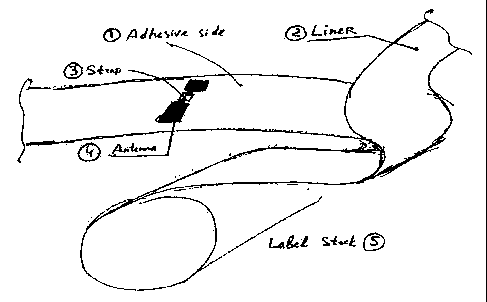
The invention provides a method of manufacturing RFID transponders for
attachment to packages that will be in transit or to packages containing, for
example, medicinal preparations, when information respecting the handling of
the
packages or the timing of removal of the medicinal preparations is required.
The
method utilizes a continuous strip of adhesive backed material, such as an
adhesive
tape supplied on a roll. As the tape is removed from the roll an anti-adhesive
material is applied to predetermined areas of the adhesive surface to render
such
areas non-adhesive. A conductive ink is coated to the non-adhesive areas to
create
spaced apart antenna pads. An RFID chip strap, carrying an RFID chip, and
having
corresponding spaced apart conductive pads is applied to the tape with the
conductive pads thereof contacting the antenna pads. The strap is secured to
the
tape through contact with the adhesive surrounding the antenna pads. Completed
transponders can be severed from the tape and applied via the adhesive thereon
to
the package as desired.


Claims

Note: Claims are shown in the official language in which they were submitted.


Claims
1. A method of manufacturing RFID transponders comprising the steps of:
providing a roll of continuous label or tape material having an adhesive
material
coating one surface thereof;
applying an anti-adhesive coating to predetermined areas of said surface so as
to
deactivate the adhesive in such areas;
printing first spaced-apart conductive pads in said areas using an
electrically
conductive ink;
permitting said conductive ink to cure; and
applying to said first spaced-apart conductive pads a pre-formed RFID chip
strap
having second electrically conductive pads at spaced-apart locations thereon
and supporting
an RFID chip between and in electrical contact with said second conductive
pads;
said strap being adhered to said label or tape material through contact with
said
adhesive material at locations adjacent said predetermined areas so as to
maintain electrical
contact between said first and second conductive pads.
2. The method of claim 1 including the step of applying ultrasonic energy to
said first
and second conductive pads to enhance electrical contact therebetween, the
conductive ink
of said conductive pads being susceptible to ultrasonic welding.
3. The method of claim 1 wherein said first conductive pads are printed so as
to have a
textured surface for exposure to said second conductive pads.

Description

Note: Descriptions are shown in the official language in which they were submitted.


CA 02528797 2005-12-01
RFID TRANSPONDER STRUCTURE OPTIMIZED FOR IN-LINE LABEL CONSTRUCTION
The present invention relates to the manufacture of RFID transponders such as
might be used with medicinal packages containing tablets, when compliance
monitoring is
required, or in other situations in which data pertaining to a shipped article
or package is to
be collected during transit for later downloading or transmission.
The present invention provides a method for manufacturing such transponders
such
that they can be readily adhered to a package, as a label, in a condition
ready for use
therewith.
SUMMARY OF THE INVENTION
In accordance with the present invention RFID transponders are manufactured
using
a continuous roll of pressure sensitive tape or other such material. The tape
is removed
from the roll, exposing the adhesive face thereof. A portion of the adhesive
surface is
coated with an anti-adhesive material and an antenna is printed, using
electrically
conductive ink, on the tape on top of the anti-adhesive coating, providing a
stable
foundation for the antenna. Typically, two spaced apart antenna pads will be
printed on the
tape. An RFID chip strap, carrying the required RFID chip, with suitable
electrical
connections, is adhered to the antenna pads so that the chip is located
between the pads
and electrical connection with the antenna pads is achieved through the strap.
For greater
adhesion, or to promote curing, the strap and pads can be subjected to
ultrasonic
vibrations.
The method of the present invention is suited to high speed automated
equipment
and represents an inexpensive procedure for creating transponders for
subsequent
assembly to packages or other articles. The completed transponders can be
severed from
tape carrying a plurality of the transponders and then adhered to the package
by way of
adhesive on the tape portion thereof surrounding the transponders
BRIEF DESCRIPTION OF THE DRAWINGS
Figure 1 is a sketch showing the basic principles of the present invention.
Figure 2 is an enlarged sketch showing the conductive antenna pads on the
adhesive
tape.
Figure 3 is an enlarged sketch showing the RFID strap in position on the
antenna
1

CA 02528797 2005-12-01
pads.
Figure 4 is a view showing ultrasonic welding of the strap to the pads.
Figure 5 is a sketch showing the RFID chip strap.
Figure 6 shows textured surface of the printing.
DESCRIPTION OF THE PREFERRED EMBODIMENTS
The following sets forth the primary embodiment of the present invention as
well as
several alternative or complementary aspects of the invention.
1. Pressure sensitive label stock adhesive is used for the strap bonding
The transponder (Fig 1) consists of an antenna 4 which is printed on the
adhesive
side 1 of delaminated label stock 5, such as adhesive tape. The label stock is
provided on a
roll thereof and stock is progressively removed from the roll as required. If
the label stock
is provided with a liner, as illustrated, the liner is continuously separated
from the adhesive
surface of the tape, so as to expose the adhesive surface. An RFID chip strap
3 is then
mounted to the antenna 4.
Antenna 4, in the form of a conductive pad, is printed using electrically
conductive
ink on top of the pressure sensitive adhesive tape after delaminating of the
stock liner.
The area of the tape on which the antenna is to be printed is initially
covered with a
printable anti-adhesive coating which promotes a stable foundation for the
conductive ink to
be transferred to.
The pressure sensitive adhesive is deactivated by the anti-adhesive coating,
so that
it no longer performs as an adhesive. The anti-adhesive coating may be applied
in line on a
printing press as a first colour and the conductive ink is printed as a second
colour.
The printed conductive pads 3 and 4 (Fig 2) are antenna areas designed for the
RFID
chip strap to be attached thereto. Conductive pads 3 and 4 have multiple
adhesion
windows 1. Each adhesion window has a central area not covered with any
coating or ink,
so that the pressure sensitive adhesive from the label stock is exposed to the
chip strap
coming on top of the pad.
The strap is bonded to the antenna through the adhesion windows and through
the
area between and around the conductive pads which is not covered with anti-
adhesive
coating (Fig 3). The strap needs to have an extended width to the sides, so
that there is
enough area for bonding outside the perimeter of the conductive pads. The
special shape of
2

CA 02528797 2005-12-01
the conductive antenna pads and of the strap will increase the probability of
a good
electrical connection and strap-to-antenna bonding during registration
variations in the in-
line process.
When the chip strap (which includes the substrate 6 (Fig 4) and its own
printed
conductive pads 5) is pushed against the conductive antenna pads (printed on
substrate 1
with anti-adhesive layer 3 and conductive ink layer 4), a stable electrical
connection is
established.
2. Ultrasonic welding is used to establish electrical connection between RFID
chip strap and
printed antenna
When welding plastics, a temperature rise in the bonding area is produced by
the
absorption of mechanical vibrations, the reflection of the vibrations in the
connecting area,
and the friction of the surfaces of the parts. The vibrations are introduced
vertically. In the
contact area, frictional heat is produced so that material plasticizes
locally, forging an
insoluble connection between both parts within a very short period of time.
The
prerequisite is that both working pieces have a near equivalent melting point.
This process could be used to bond printed conductive pads 5 of the RFID chip
strap
to printed conductive pads 4 of the RFID antenna (Fig 4). The conductive ink
which is used
to print antenna pads and chip strap pads has the ability to be bonded
ultrasonically.
The pad design and location is very important in ultrasonic welding, so that
it will be
accomplished in such a way that there is no interference between welding of
joints (the joint
between the strap pad and antenna pad) which are getting welded.
Ultrasonic welding of the strap to the antenna pads can be used on its own or
it can
be used in conjunction with the first-described method of adhesive bonding, to
improve or
speed up adhesive curing. Ultrasonic welding also enhances electrical
conductivity at the
junction of the conductive pads of the strap and the antenna.
3. Linear array design of antenna with capacitive coupled fingers, one of
which has the RFID
chip strap on it
In the case of RFID UHF antennas, characteristics such as high gain, beam
scanning
or steering capability are possible when discrete fingers are combined to form
arrays. The
center points of the elements (fingers) are adjusted to coincide with the
voltage maxima of
the transmission line feeder so that each element appears as a small load.
3

CA 02528797 2005-12-01
A single finger with strap on it works as an on/off switch for the antenna.
The RFID strap could be attached to a printed antenna array structure without
having any electrical connection to any antenna element. Such RFID transponder
structure
has the advantage of simplified strap attachment in-line with antenna
printing.
The bandwidth and coupling parameters could be adjusted by tapering the width
of
rectangular elements such that it forms a diamond shaped patch.
4. Forming of 3D textured surface of antenna during of printing process
There is a significant improvement of RFID antenna performance if the antenna
surface has 3D textured surface. The sizes and shapes of 3D surface elements
need to be
tuned to the antenna resonance frequency and bandwidth.
Flexographic and gravure printing processes give all required means to control
size
and shape of antenna surface texture elements. For example plate screening
could be used
to control depth and shape of antenna surface texture. Ink viscosity, softness
of plate
material and of sticky back, as well as printing speed are other variables
affecting 3D
antenna surface structure. The antenna could be printed on a textured
substrate which has
surface parameters tuned to the antenna resonance. See for example Fig. 6.
Printing on a substrate with variable ink absorption of the surface gives the
same
effect to the textured substrate. Ink absorption could be controlled by a non-
absorbing
material mask printed as an under layer.
4

Representative Drawing
A single figure which represents the drawing illustrating the invention.
Administrative Status

2024-08-01:As part of the Next Generation Patents (NGP) transition, the Canadian Patents Database (CPD) now contains a more detailed Event History, which replicates the Event Log of our new back-office solution.

Please note that "Inactive:" events refers to events no longer in use in our new back-office solution.

For a clearer understanding of the status of the application/patent presented on this page, the site Disclaimer , as well as the definitions for Patent , Event History , Maintenance Fee  and Payment History  should be consulted.

Event History

Description Date
Application Not Reinstated by Deadline 2010-12-01
Time Limit for Reversal Expired 2010-12-01
Deemed Abandoned - Failure to Respond to Maintenance Fee Notice 2009-12-01
Letter Sent 2008-03-19
Inactive: Transfer reinstatement 2008-02-12
Reinstatement Requirements Deemed Compliant for All Abandonment Reasons 2008-02-12
Inactive: Declaration of entitlement - Formalities 2008-02-12
Inactive: Status info is complete as of Log entry date 2007-06-05
Application Published (Open to Public Inspection) 2007-06-01
Inactive: Cover page published 2007-05-31
Inactive: Abandoned - No reply to Office letter 2007-03-05
Inactive: Filing certificate - No RFE (English) 2006-11-15
Correct Inventor Requirements Determined Compliant 2006-11-15
Inactive: First IPC assigned 2006-08-31
Inactive: IPC assigned 2006-08-31
Inactive: Filing certificate correction 2006-02-10
Inactive: Courtesy letter - Evidence 2006-01-24
Filing Requirements Determined Compliant 2006-01-19
Inactive: Filing certificate - No RFE (English) 2006-01-19
Application Received - Regular National 2006-01-17
Small Entity Declaration Determined Compliant 2005-12-01

Abandonment History

Abandonment Date Reason Reinstatement Date
2009-12-01

Maintenance Fee

The last payment was received on 2008-10-31

Note : If the full payment has not been received on or before the date indicated, a further fee may be required which may be one of the following

  • the reinstatement fee;
  • the late payment fee; or
  • additional fee to reverse deemed expiry.

Please refer to the CIPO Patent Fees web page to see all current fee amounts.

Fee History

Fee Type Anniversary Year Due Date Paid Date
Application fee - small 2005-12-01
MF (application, 2nd anniv.) - small 02 2007-12-03 2007-12-03
Reinstatement 2008-02-12
MF (application, 3rd anniv.) - small 03 2008-12-01 2008-10-31
Owners on Record

Note: Records showing the ownership history in alphabetical order.

Current Owners on Record
INTELLIGENT DEVICES INC.
Past Owners on Record
JAMES NEILSON
MICHAEL PETERSEN
MYKOLA SHERSTYUK
Past Owners that do not appear in the "Owners on Record" listing will appear in other documentation within the application.
Documents

To view selected files, please enter reCAPTCHA code :


To view images, click a link in the Document Description column. To download the documents, select one or more checkboxes in the first column and then click the "Download Selected in PDF format (Zip Archive)" or the "Download Selected as Single PDF" button.

List of published and non-published patent-specific documents on the CPD .

If you have any difficulty accessing content, you can call the Client Service Centre at 1-866-997-1936 or send them an e-mail at CIPO Client Service Centre.


Document
Description 
Date
(yyyy-mm-dd) 
Number of pages   Size of Image (KB) 
Description 2005-12-01 4 172
Abstract 2005-12-01 1 23
Claims 2005-12-01 1 29
Drawings 2005-12-01 3 112
Representative drawing 2007-05-28 1 10
Cover Page 2007-05-28 1 46
Filing Certificate (English) 2006-01-19 1 157
Request for evidence or missing transfer 2006-12-04 1 101
Filing Certificate (English) 2006-11-15 1 158
Courtesy - Abandonment Letter (Office letter) 2007-04-16 1 166
Reminder of maintenance fee due 2007-08-02 1 112
Notice of Reinstatement 2008-03-19 1 171
Courtesy - Abandonment Letter (Maintenance Fee) 2010-01-26 1 171
Reminder - Request for Examination 2010-08-03 1 120
Correspondence 2006-01-19 1 26
Correspondence 2006-02-10 2 116
Correspondence 2008-02-12 2 66