Note: Descriptions are shown in the official language in which they were submitted.
CA 02528977 2005-12-09
WO 2004/112225 PCT/US2004/018304
-1-
HIGH EFFICIENCY OFF-LINE LINEAR POWER SUPPLY
BACKGROUND OF THE INVENTION
The present invention relates to power supplies. More particularly, the
present invention relates to catear power supplies 'used to provide power to
electronic circuits and which may receive their power across a circuit element
disposed in a power line. For example, two wire lamp dimmers which are
disposed in the hot side of an AC line are used to power lamp loads and vary
the
lamp intensity. The neutral line is provided directly to the lamp load and is
not
connected to the dimmer. In this way, a dimmer can be substituted for a single
or
multiple pole switch. The problem arises in such situations that if the dimmer
includes additional circuitry, for example, control circuits or in some more
complex systems, microprocessors and radio frequency circuits for transmitting
and receiving control and status information, it is necessary to derive the
power
for those circuits solely from the hot line, since the neutral is not
available. This
can be done in a conventional way by providing a voltage dropping circuit in
the
hot line. However, this has a deleterious effect on the load and, in
particular,
would reduce the maximum brightness of the lamp c~nnected to the dimmer.
The catear circuit was developed to draw current from the hot AC line in a
two wire dimmer configuration. As shown in Fig. 2, in a conventional dimmer, a
triac (not shown) is turned on at a particular point in.the AC half cycle and
turns
off prior to the next zero crossing. Fig. 2 shows both the AC waveform (marked
AC) and a full wave rectified version of the AC waveform wherein the negative
going half cycles are inverted by a full wave rectifier. The inverted half
cycle is
marked DC in Fig. 2. In the first half cycle, the regions when the triac is
typically
off are shown at 1 and 3. The region marked 2 is when the triac is on. As well
knovcni, dimmers of this type are known as phase-control dimmers and the
intensity of the lamp load is controlled by varying the cut-in point of the
triac,
CA 02528977 2005-12-09
WO 2004/112225 PCT/US2004/018304
-2-
thus varying the amount of power delivered to the load, and thus the intensity
or
brightness level of the lamp load. After the triac turns on (region 2), the
voltage
across the dimmer is substantially zero and it is difficult to obtain power
from the
dimmer itself at this time in the absence of any voltage dropping circuit,
which,
for the reasons discussed above, is undesirable. However, power can be taken
from the AC line in the time period before the triac turns on (region 1)
because at
this point in time, the lamp is off. Similarly, power may be obtained from the
AC
line after the triac goes off before the next zero crossing (region 3). As
shown in
Fig. 2, the distinctive "catears" of regions 1 and 3 of the waveform shown
both
before the triac turns on and after it turns off, give the circuit its name.
It is
during these time periods, i.e., during the "catears" that power can be
derived
from the AC hot line without interfering with the dimmer operation.
Fig. 1 shows a conventional catear circuit. The catear circuit is wired to
receive power from a rectifier circuit (RECT), for example, a full wave
rectifier,
which is wired across a portion of the dimmer circuit to receive rectified AC
power. The rectifier provides current substantially only during the catear
regions
because when the triac of the dirmner circuit is on, there is substantially
zero
voltage across the dimmer. As shown in Fig. 1, a transistor Q206, which may be
an FET, is turned on during the catear portions of the rectified AC, i.e.,
before the
triac turns on and after the triac turns off again. The gate of transistor
Q206 is
provided with a voltage sufficient to turn it on via resistors 8210, 8212 and
8220. When Q206 goes on, a charging capacitor C262 is charged via resistor
8280 and diode D252. The output across capacitor C262 is provided to a voltage
regulator circuit, for example, a linear regulator U203 which provides a
substantially constant DC output to power the circuits connected thereto.
Accordingly, when the rectified line voltage is lower than a selected
voltage, the charging transistor Q206 conducts to allow charging of the energy
storage capacitor C262. The rate of charge of the capacitor is determined by
resistor 8280.
CA 02528977 2005-12-09
WO 2004/112225 PCT/US2004/018304
-3-
When the rectified line voltage exceeds a predetermined value, then
transistor Q204 is turned on by the voltage divider formed by resistors 8214,
8221 and 8276. When transistor Q204 turns on, which time can be set by
voltage divider circuit comprising resistors 8214 and 8221 so that it is just
prior
to the time when the triac of the dimmer circuit turns on, the voltage at the
collector of Q204 goes substantially to circuit common, thereby bringing the
gate
of Q206 substantially to circuit common and turning Q206 off so that Q206
stops
charging capacitor C262 during the time when the triac is on.
Accordingly, capacitor Q262 is utilized as a charge storage element to
charge up during the time prior to the triac turning on during the catear
portion 1
of the rectified AC line voltage. During the time when the triac is on (region
2),
power for the associated electronic circuits connected to the output of
regulator
Q203 is provided by the storage capacitor C262. When the triac turns off in
region 3 of Fig. 2, the voltage at the base of Q204 will again be below its
turn-on
threshold and Q206 will again provide charging current to capacitor C262
during
catear region 3.
In addition, a circuit comprising transistor Q252 is also provided to sense
an overcurrent condition. Should an overcurrent be detected across resistor
8280,
transistor Q252 turns on, thus reducing the gate voltage of transistor Q206 to
near
zero and turning it off. In addition, a bus regulation circuit comprising
zener
diode D207 and resistor 8275 is provided. If the voltage across storage
capacitor
0262 rises too high, the zener diode D207 will avalanche, raising the voltage
across resistor 8276 and turning on Q204 which will thus reduce the gate
voltage
to transistor Q206, turning it off. Accordingly, if C262 exceeds a
predetermined
voltage, Q206 will be turned off in that instance also to stop charging C262.
A problem arises with the conventional catear circuit in that its efficiency
is impaired because transistor Q206 operates for a substantial portion of the
time
during the "catears" in its linear mode of operation, that is, it is not
saturated.
This is due to the drive voltage rising with the line, as well as other
factors. It is
CA 02528977 2005-12-09
WO 2004/112225 PCT/US2004/018304
-4-
thus turned on too slowly which causes the switching FET to operate in the
linear
region for much of the charging time, thereby dissipating power in the FET
itself.
Accordingly, it is desirable to improve the prior art catear power supply
circuit to improve its efficiency and, in particular, to improve its
efficiency by
ensuring that the switching device that charges the charging capacitor
operates in
its saturated region, thereby dissipating the least amount of power in the
switching device and improving the overall efficiency of the catear power
supply.
SUMMARY OF THE INVENTION
The above and other objects of the present invention are achieved by a
power supply circuit comprising: a first switching device having a control
terminal and a control terminal switching threshold, the first switching
device
charging current from a voltage source into a charge storage element, a
control
circuit controlling an on/off operation of the first switching device whereby
the
first switching device is turned on when the voltage of the voltage source is
below a predetermined level and turned off when the voltage of the voltage
source is above the predetermined level, a control voltage supply circuit
providing a control voltage to the control terminal of the first switching
device
substantially in excess of the switching threshold in response to the control
circuit
when the voltage of the' voltage source is below the predetermined voltage
thereby to drive the switching device on in a saturated region of operation;
and a
charge storage element for providing an output voltage of the power supply.
It is desirable to drive the first switching device into saturation, whereby
the voltage across the switching device~is reduced beyond its voltage drop in
the
linear region of operation, thus increasing power supply efficiency.
The above and other objects are also achieved by a catear power supply
circuit comprising a first switching transistor having a control terminal and
a
control terminal switching threshold, the first switching transistor charging
current from a voltage source into a charge storage capacitor, a control
circuit
controlling an on/off operation of the first switching transistor whereby the
first
CA 02528977 2005-12-09
WO 2004/112225 PCT/US2004/018304
-S-
switching transistor is enabled to be turned on when the voltage of the
voltage
source is below a predetermined level and is turned off when the voltage of
the
voltage source is above the predetermined level, a control voltage supply
circuit
providing a control voltage substantially in excess of the switching
threshold, the
control voltage being supplied to the control terminal of the first switching
transistor by the control circuit such that when the voltage of the voltage
source is
below the predetermined level, the control voltage is supplied to the control
terminal of the first switching transistor thereby to drive the first
switching
transistor on in a saturated region of operation and when the voltage of the
voltage source is above the predetermined threshold, the control voltage is
not
supplied to the control terminal, thereby turning the first switching
transistor off;
and a charge storage capacitor for providing an output voltage of the power
supply.
The above and other objects are furthermore achieved by a lighting
dimmer comprising an electronic lamp dimmer circuit providing power to a lamp
load, a catear power supply coupled to the electronic lamp dimmer circuit for
providing power to electronic circuits of the lighting dimmer, the catear
power
supply circuit comprising a switching device having a control terminal and a
control terminal switching threshold, the switching device charging current
from
a voltage source into a charge storage element, a control circuit controlling
the
on/off operation of the switching device whereby the switching device is
turned
on when the voltage of the voltage source is below a predetermined level and
turned off when the voltage of the voltage source is above the predetermined
level, a control voltage supply circuit providing a control voltage to the
control
terminal of the switching device substantially in excess of the switching
threshold
when the voltage of the voltage source is below the predetermined level
thereby
to drive the switching device on in a saturated region of operation; and a
charge
storage element for providing an output voltage of the power supply.
The above and other objects are also achieved by a method of providing
power to an electronic circuit in a two wire dimmer connecting a hot line of
an
CA 02528977 2005-12-09
WO 2004/112225 PCT/US2004/018304
-6-
AC network to a lamp load, the method comprising obtaining power from the two
wire dimmer during regions of an AC waveform formed across a portion of a
circuit of the dimmer when a phase cut switching device of the dimmer
providing
power to the lamp load is substantially off; driving a switching device
providing
charging current to a charge storage capacitor on in a saturated region of
operation of the switching device when a voltage from a voltage source
developed in the dimmer from the AC waveform is less than a predetermined
level, and turning the switching device off when the voltage is .above the
predetermined level, and providing a voltage across the charge storage device
as
an output voltage.
Although the present invention is described herein for use with respect to
lamp loads, the invention can also be used with other loads, e.g., motors and
other
loads. In addition, various lamps can be employed as loads, and the invention
is
not limited to incandescent lamp loads but may be used with fluorescent and
other gas discharge lamps, without limitation. Further, the invention may be
used
in "non-dimmer" or other applications where both a hot and neutral are
available.
Other features and advantages of the present invention will become
apparent from the following detailed description of the invention which refers
to
the accompanying drawings.
BRIEF DESCRIPTION OF THE DR.AWINGfS~
The invention will now be described in greater detail in the following
detailed description with reference to the drawings in which:
Fig. 1 shows a prior art catear power supply;
Fig. 2 shows both the rectified and unrectified AC line waveform showing
the catear portions during which the triac is turned off;
Fig. 2A shows schematically how the power supply of the present
invention is disposed in a circuit including a two wire dimmer connected to a
load
and an AC network;
CA 02528977 2005-12-09
WO 2004/112225 PCT/US2004/018304
_7_
Fig. 2B shows the power supply of Fig. 2A and the electronic circuits of
the dimmer which it powers;
Fig. 3 is a block diagram of the power supply according to the present
invention;
Fig. 4 is a schematic circuit diagram of the power supply according to the
present invention; and
Figs. SA-SE show the gate-drain voltage across the switching FET
charging the storage capacitor, the voltage across the storage capacitor, the
input
current to the power supply and the gate voltage to the switching FET for
respective load currents of SOmA, 75mA, 100mA, 125mA, and 150mA with a
120 VAC input.
DETAILED DESCRIPTION OF THE EMBODIMENT OF THE INVENTION
With reference to the drawings, Fig. 2A shows a dimmer incorporating the
power supply (PS) according to the present invention. As shown, the dimmer
includes a triac and its associated dimmer control circuitry as well known to
those
of skill in the art, as well as additional circuitry to be powered by the
power
supply. As shown in Fig. 2A, the dimmer is wired into the hot side (H) of the
AC
line and provides a dimmed hot (DH) output to the load comprising a lamp load.
Although a lamp load is shown, the circuit could be employed with other loads,
for example, a motor, in which case the speed of the motor is being
controlled.
As shown, the neutral (N> of the AC line is not connected to the dimmer so it
is
not possible to obtain power for the circuits in the dimmer directly across
the AC
line. Instead, as discussed above, the power supply (PS) must obtain its power
across some portion of the dimmer circuit itself.
Fig. 2B shows how the power supply of Fig. 2A is coupled to the hot AC
line and provides power to various low voltage control circuits contained
within
the dimmer, for example, a microprocessor uP, an RF circuit, various displays
and the tx-iac dimmer circuit itself. For example, the power supply according
to
the present invention may be employed with dimmers that incorporate control
CA 02528977 2005-12-09
WO 2004/112225 PCT/US2004/018304
_g_
circuits that receive and provide control and status information via radio
frequencies. An example of such a system is the Lutron RF seeTouch~ system
and for less complex systems, the Lutron RadioRA~ system. In both of these
systems, lighting zones in various parts of a building can be controlled from
a
central or other locations via radio frequency signals.
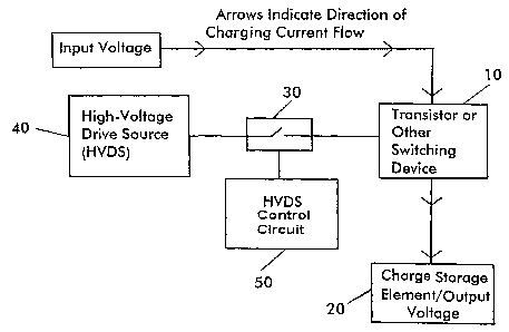
Fig. 3 is a block diagram of the power supply according to the invention.
The circuit includes a switching device 10 coupled to a source of input
voltage, a
charge storage element 20 providing an output voltage, a control switching
device
30 for controlling the on/off operation of the main switching device 10, a
control
voltage supply circuit comprising a high voltage drive source circuit 40 for
driving the charging switch 10 into saturation when the switch 10 is
controlled
on, and a control circuit 50 for controlling the switching circuit 30 to
control the
on/off status of switching device 10.
Turning now to Fig. 4, a circuit diagram for the power supply according to
the present invention is shown. Switching circuit 10 comprises a switching
transistor such, as an FET Q11 having its drain connected to a voltage source
V+
and its source connected through a resistor R9 and diode D 17 to a charging
capacitor C4 in charge of storage circuit 20. Voltage source V+ may be
provided
from a full wave rectifier bridge (RECT), as shown, connected across some
portion of the dimmer. The gate of transistor Q11 is coupled through resistors
R32, R55 and R52 to a high voltage drive source circuit 40. The high voltage
drive source circuit 40 includes a resistor R49, diode D60, capacitor C16 and
a
zener diode Zl connected as shown and coupled between the voltage source V+
and Vc which is the voltage across storage capacitor C4 and ground.
Illustratively, capacitor C 16 may be .luf, resistor R49 may be 110 kohms and
diode Z1 may be a 39 volt zener, so that approximately 40V may be developed
across C16.
The control circuit 50 comprises control circuit portions SOA, SOB, SOC
and SOD. Portion SOA comprises a voltage divider comprising resistors R3 and
R4. The voltage divider output is connected to the base of a transistor Q14,
CA 02528977 2005-12-09
WO 2004/112225 PCT/US2004/018304
-9-
forming the switching circuit 30. Furthermore, the base of transistor Q14 is
connected to circuit SOB which comprises a bus regulation circuit connected
between the base of transistor Q14 and the anode of diode D17 connected in
series with storage capacitor C4.
In addition, control circuit 50 also includes an overcurrent protection and
current limiting circuit SOC and a latch circuit SOD..
The circuit operates as follows. Transistor Q11 charges capacitor C4
through resistor R9 and diode D17. Diode D17 prevents discharging of capacitor
C4 when Ql 1 is off. The gate of transistor Ql 1 is provided with gate voltage
via
gate voltage supply circuit 40 and resistors R52, R55 and R32. Gate voltage
supply circuit 40 is connected between voltage source V+ and voltage Vc across
capacitor C4. Since the voltage across C4 is substantially lower than the
voltage
on the bus V+, capacitor C16 in circuit 40 immediately begins to charge via
resistor R49 and diode D60 as the rectified AC voltage increases during the
catear
region 1 of Fig. 2. Zener diode Z1 limits the voltage across the capacitor C16
and ensures that the capacitor C16 charges quickly because it acts as a
current
divider drawing current from V+ to quickly reach its avalanche voltage.
Capacitor C16 charges quickly through diode D60 and resistor R49, and the
voltage across capacitor C16 plus the voltage across capacitor C4 is provided
to
the gate of transistor Ql 1 via resistors R52, R55 and R32, driving transistor
Q11
into the saturated region very quickly. As an exemplary embodiment, the gate
voltage provided to transistor Q11 may be approximately 15 volts, thus quickly
driving transistor Q11 into saturation. A zener diode Z2 is provided to
prevent
the gate voltage from exceeding a predetermined safe level to protect FET Q11,
for example, to maintain the gate voltage below about 25 volts.
Diode D60 prevents discharge of capacitor C16 when voltage V+ drops to
near zero when the triac turns on.
Once transistor Q11 goes on, it is in its saturated region and the capacitor
C4 is charged with minimal loss in transistor Q11. The charged voltage across
capacitor C4 is provided to a voltage regulator U2, for example, a
conventional
CA 02528977 2005-12-09
WO 2004/112225 PCT/US2004/018304
-10-
linear regulator, similarly as in the prior art, and the output of U2 is
provided to
power the various electronic circuits.
Transistor Q14 performs the function of switch 30 in the block diagram of
Fig. 3. As soon as the voltage V+ exceeds a predetermined level, Q14 is turned
on (the triac turns on at some time thereafter), thus driving the gate of Q11
low
via resistors R55 and R32, and turning Q11 off, preventing charging during the
period of time when the dimmer triac turns on, thereby preventing drawing
current away from the dimmer and lamp load during this time.
Transistor Q14 is turned on by the voltage divider circuit SOA comprising
resistors R3 and R4. .
In addition, circuit SOD includes a latch circuit comprising transistor Q25.
In the circuit shown, the transistor Q25 is a PNP transistor. Q25 functions to
latch transistor Q14 on and therefore the FET Q11 off. When Q14 is turned on
by
the V+ bus voltage exceeding a predetermined level, the collector voltage of
Q14
drops. The collector of Q14 is connected to the base PNP transistor Q25 by
resistor R54. When~the collector of Q14 drops, Q25 turns on thereby increasing
the voltage drop across resistor R4 thus ensuring that transistor Q14 latches
on.
After the triac of the dimmer turns on, the voltage on bus V+ drops
substantially to zero, so no charging current is delivered to the charge
storage
capacitor C4 during this time, which corresponds to region 2 of Fig. 2.
Circuit 50 also includes circuit SOB which comprises a bus regulation
circuit. Should the voltage across capacitor C4 increase above a preset level,
zener diode Z3 avalanches, thereby increasing the voltage across the resistor
R4
and turning transistor Q14 on. This could occur, for example, during the
catear
portions of the input waveform (regions 1 and 3 of Fig. 2) when capacitor C4
is
charging should the charging voltage across capacitor C4 increase_to levels
above
a predetermined voltage.
Circuit 50 also includes an overcurrent protection and current limiting
circuit SOC. Resistor R9 limits the current through the FET at all times. In
addition, transistor Q26 is connected to resistor R9 such that should the
voltage
CA 02528977 2005-12-09
WO 2004/112225 PCT/US2004/018304
-11-
across resistor R9 exceed the threshold of Q26, transistor Q26 will turn on
thereby driving the gate of transistor Q11 toward its source and turning
transistor
Q11 off in the event of an overcurrent.
Once the triac of the dimmer turns off, the voltage across bus V+ is
determined by the catear waveform of region 3 of Fig. 2, and, as soon as the
voltage V+ drops below a certain level so that voltage divider SOA provides a
voltage insufficient to keep transistor Q14 on, Q14 turns off, thus turning on
Q11
and again charging current into capacitor C4 during catear region 3 of Fig. 2.
The present invention thus provide a power supply of the catear type
which is highly efficient because losses in the switching device charging the
charge storage element are reduced by ensuring that the switching device, when
on, is operating in its saturated region. In contrast, prior art catear
topologies turn
the switching device on in dependence on the AC line voltage which dissipates
considerably more energy since the FET is not saturated but instead operating
in
its linear region. The present invention provides for FET saturation at low
line
voltages, which leads to greater efficiency.
Another advantage of the present circuit over other possible power supply
circuits is that the switching device operates at a low frequency. In
contrast, prior
art switching power supplies operate at high frequencies creating substantial
RF
noise which can interfere with RF control circuits with which the present
invention can operate as well as generally radiating substantial EMI which
must
be shielded or otherwise reduced .
Figs. SA-SE show waveforms of the gate-drain voltage across FET Q11,
the voltage across capacitor C4, the input current into the rectifier and the
gate
voltage of FET Q11 measured between the gate and the circuit common ground
connection. Each waveform is based upon a network voltage of 120 volts AC.
Fig. 5A is for a load current of 50 mA; Fig. 5B shows the waveforms for a load
of
75 mA; Fig. SC shows the waveform for a load of 100 mA; Fig. SD shows the
waveforms for a load of 125 mA; and Fig. SE shows the waveforms for a load of
150 mA.
CA 02528977 2005-12-09
WO 2004/112225 PCT/US2004/018304
-12-
As can be seen from the waveforms, the gate waveform to transistor Q11
has a very sharply defined rising edge with the voltage rising quickly to
about 15
volts, thus driving the FET Q11 into saturation very quickly. The gate voltage
rises high enough to turn the FET on quickly into saturation . The V+ voltage
bus
ranges from about 50 volts down to about 45 volts. The capacitor bus voltage
across capacitor C4 ranges between 8.5 to 7.5 volts at 150 mA load and the
input
current essentially follows the line current.
Although the present invention has been described in relation to particular
embodiments thereof, many other variations and modifications and other uses
will become apparent to those skilled in the art. Therefore, the present
invention
should be limited not by the specific disclosure herein, but only by the
appended
claims.