Note: Descriptions are shown in the official language in which they were submitted.
CA 02529579 2005-12-14
WO 2005/012900 PCT/US2004/019652
BIOSENSOR WITH MULTIPLE ELECTRICAL
FUNCTIONALITIES
REFERENCE TO RELATED APPLICATIONS
This application is related to applications entitled TEST STRIP WITH
SLOT VENT OPENING ("Slot Vent Opening") (attorney docket no. 7404-
567), METHOD OF MAKING A BIOSENSOR (attorney docket no. 7404-
480), METHOD AND REAGENT FOR PRODUCING NARROW,
HOMOGENEOUS REAGENT STRIPES ("Reagent Stripes") (attorney
docket no. 7404-475), DEVICES AND METHODS RELATING TO
ELECTROCHEMICAL BIOSENSORS (attorney docket no. 7404-569),
SYSTEM AND METHOD FOR QUALITY ASSURANCE OF A
BIOSENSOR TEST STRIP ("Quality Assurance") (attorney docket no. 7404-
456), SYSTEM AND METHOD FOR CODING INFORMATION ON A
BIOSENSOR TEST STRIP ("Coding Information") (attorney docket no.
7404-562), DISPENSER FOR FLATTENED ARTICLES ("Dispenser")
(attorney docket no. 7404-591), all of which have been filed on even date
herewith and which are all incorporated herein by reference in their
entireties.
This application also is related to an application entitled SYSTEM AND
METHOD FOR ANALYTE MEASUREMENT USING DOSE
SUFFICIENCY ELECTRODES, filed October 17, 2003 and given serial no.
10/687,958 ("Dose Sufficiency"), which is incorporated herein by reference in
its entirety.
CA 02529579 2005-12-14
WO 2005/012900 PCT/US2004/019652
2
FIELD OF THE INVENTION
The present invention relates generally to devices, systems, and
methods for measuring analytes from biological samples, such as from a
sample of bodily fluid. More particularly, the present invention relates to
electrically operable biosensors.
CA 02529579 2005-12-14
WO 2005/012900 PCT/US2004/019652
3
BACKGROUND
Measuring the concentration of substances, particularly in the presence
of other, confounding substances ("interferents"), is important in many
fields,
and especially in medical diagnosis and disease management. For example,
the measurement of glucose in bodily fluids, such as blood, is crucial to the
effective treatment of diabetes.
Multiple methods are known for measuring the concentration of
analytes such as glucose in a blood sample. Such methods typically fall into
one of two categories: optical methods and electrochemical methods. Optical
methods generally involve absorbance, reflectance or laser spectroscopy to
observe the spectrum shift in the fluid caused by the concentration of the
analytes, typically in conjunction with a reagent that produces a known color
when combined with the analyte. Electrochemical methods generally rely
upon the correlation between a charge-transfer or charge-movement property
of the blood sample (e.g., current, interfacial potential, impedance,
conductance, and the like) and the concentration of the analyte, typically in
conjunction with a reagent that produces or modifies charge-carriers when
combined with the analyte. See, for example, U.S. Patent Nos. 4,919,770 to
Preidel, et al., and 6,054,039 to Shieh, which are incorporated by reference
herein in their entireties.
An important limitation of electrochemical methods of measuring the
concentration of a chemical in blood is the effect of confounding variables on
the impedance of a blood sample. For example, the geometry of the blood
sample must correspond closely to that upon which the impedance-to-
concentration mapping function is based.
The geometry of the blood sample is typically controlled by a sample-
receiving chamber of the testing apparatus in which the fluid sample is
received and held during its analysis. In the case.of blood glucose meters,
for
example, the blood sample is typically placed onto a disposable test strip or
biosensor that plugs into the meter. The test strip may have a sample chamber
to define the geometry of the sample. Alternatively, the effects of sample
CA 02529579 2005-12-14
WO 2005/012900 PCT/US2004/019652
4
geometry may be limited by assuring an effectively infinite sample size. For
example, the electrodes used for measuring the analyte may be spaced closely
enough so that a drop of blood on the test strip extends substantially beyond
the electrodes in all directions. Regardless of the strategy used to control
sample geometry, typically one or more dose sufficiency electrodes are used to
assure that a sufficient amount of sample has been introduced into the sample
receiving chamber to assure an accurate test result.
Other examples of limitations to the accuracy of blood glucose
measurements include variations in blood chemistry (other than the analyte of
interest being measured). For example, variations in hematocrit (concentration
of red blood cells) or in the concentration of other chemicals, constituents
or
formed elements in the blood, may affect the measurement. Variation in the
temperature of blood samples is yet another example of a confounding variable
in measuring blood chemistry. In addition, certain other chemicals can
influence the transfer of charge carriers through a blood sample, including,
for
example, uric acid, bilirubin, and oxygen, thereby causing error in the
measurement of glucose.
Efforts to improve test strips have been mainly directed to making
them smaller, faster, and require less sample volume. For example, it is
desirable for electrochemical biosensors to be able to analyze as small a
sample as possible, and it is therefore necessary to minimize the size of
their
parts, including the electrodes. Traditionally, screen-printing, laser
scribing,
and photolithography techniques have been used to form miniaturized
electrodes. These methods are undesirably time-consuming, however, and
screen-printing or laser scribing technologies pose limitations on the edge
quality of the electrical patterns formed, such that gap widths between
electrical elements normally must be 75 microns or more. Further, some of
these techniques make it unworkable on a commercial scale to remove more
than a small fraction, e.g., more than 5-10% of the conductive material from a
substrate to form an electrical pattern.
CA 02529579 2005-12-14
WO 2005/012900 PCT/US2004/019652
The electrode structures in available electrochemical test strips made
by these techniques typically have one or perhaps two pairs of electrodes, and
the measurements obtained by these electrode structures are quite sensitive to
the interferents discussed above. Thus, the signal produced by the analyte
desired to be analyzed must be deconvoluted from the noise produced by the
interfering substances. Many approaches have been employed to
attenuate/mitigate interference or to otherwise compensate or correct a
measured value. Often, multiple design solutions are employed to adequately
compensate for the sensitivities associated with the chosen measurement
method.
One approach involves removing interfering materials such as blood
cells from the fluid sample before it reaches the electrodes by using perm-
selective andlor size-selective membranes, filters or coatings. Multiple
layers
of membranes are often laminated together to achieve the ultimate goal of
delivering a fluid to the electrodes which contains only low levels of
interferents. Unfortunately, however, this approach suffers from incremental
costs of goods, viz., coatings and membranes that must often be pre-treated
prior to assembly. It also incurs additional manufacturing process steps that
further increase manufacturing cost and complexity while decreasing the
speed of manufacture. This approach addresses the attenuation problem by
increasing the complexity and cost of the test strip, thereby reducing the
burden of the meter which reads the strips.
Another general approach involves the use of sophisticated excitation
and signal processing methods coupled with co-optimized algorithms. While
simpler, less complex test strip architectures and manufacturing processes may
be realized, instrumentation costs, memory and processor requirements,
associated complex coding, and calibrated manufacturing techniques are all
increased by this approach. Systems employing this approach address the
attenuation problem by placing a higher computational burden on the meter
that reads the strips.
CA 02529579 2005-12-14
WO 2005/012900 PCT/US2004/019652
6
Yet another more recent approach involves neither the strip nor
instrumentation, per se, but rather exploits the measurement methodology. An
example of this approach is the use of a coulometric method to attenuate the
influence of hematocrit and temperature. This coulometric approach,
however, requires a tight manufacturing tolerance on the volume of the sample
receiving chamber in the test strips produced, since the entire sample is used
during the analysis. Additionally, commercially available test strips using
this
technology require two separate substrates printed with electrodes, which
further increases manufacturing costs. The requirement that much of the
sample volume be interrogated may also limit test speed. Further, this
approach requires relatively large electrodes to provide significant
electrolysis
of the sample in a relatively short time in order to estimate the "endpoint"
of
the coulometric detection.
It is also well known to those skilled in the art that all of the above
approaches are further supported by the initial design of reagent systems. In
the detection of glucose, for example, this may involve the use of selective
redox mediators and enzymes to overcome the detrimental influence of redox-
active species or the presence of other sugars.
It would be desirable to provide a simpler, less costly method for
attenuating the influence of interferents, in a manner that does not suffer
the
demerits associated with the general approaches currently in wide use. It
would also be desirable to provide a more functional, robust and user-friendly
system for analyzing fluid samples, but without increasing the costs.
CA 02529579 2005-12-14
WO 2005/012900 PCT/US2004/019652
7
SUNINIARY OF THE INVENTION
The present invention provides a biosensor having multiple electrical
functionalities located both within and outside of the measurement zone in
which the fluid sample is interrogated. Incredibly small and complex
electrical patterns with high quality edges provide electrical functionalities
in
the biosensor and also provide the electrical wiring for the various other
electrical devices provided in the inventive biosensor. In addition to a
measurement zone with various electrode functionalities, biosensors of the
present invention may be provided with a user interface zone, a digital device
zone and/or a power generation zone.
The inventors of the present invention have taken an entirely different
approach than the schemes discussed above for mitigating interference or
otherwise correcting a value measured by a test strip. Their novel approach
focuses upon (1) enhancing the quality and complexity of the electrical
patterns formed on a biosensor, (2) significantly reducing the size of these
electrical patterns, and at the same time (3) increasing production speeds
while
(4) reducing manufacturing costs. This approach decreases the computational
burden and associated cost of the instruments that read the strips while at
the
same time adding accurate yet cost-effective functionalities to the biosensors
themselves.
In one form thereof, the present invention provides a biosensor for
analyzing a fluid sample. The biosensor includes a biosensor body that
defines a measurement zone having a sample receiving chamber in which is
disposed a measurement electrode for detecting the presence or concentration
of an analyte in the fluid sample. The measurement zone also includes a
reagent that reacts with the fluid sample. The biosensor body further defines
a
user interface zone in which is disposed an electrically driven signal
generator
which emits a visible, audible or tactile signal upon occurrence of a
triggering
event.
In one preferred form, the signal generator comprises a light positioned
on the test strip body which illuminates (or turns off) upon the occurrence of
CA 02529579 2005-12-14
WO 2005/012900 PCT/US2004/019652
8
the triggering event. In another preferred form the signal generator comprises
a light disposed proximate the sample receiving chamber and which
illuminates the sample receiving chamber upon the occurrence of the
triggering event. In another preferred form, the signal generator is a
numerical
display.
Any number of occurrences can constitute a "triggering event,"
including but not limited to insertion of the strip into a meter, a sufficient
size
dose being received in the sample receiving chamber, malfunction of test, non-
functional test strip, etc. Furthermore, there may be a delay between the
occurrence of the triggering event and the signal generator emitting the
signal.
In another preferred form, the signal generator comprises an electrode
set on which the OLED is coated. More preferably, the electrode set
comprises a micro-electrode array with at least two electrode fingers having a
gap of less than about 5 microns between them.
In another preferred form, the biosensor also includes a power
generation zone in which is disposed a power generator. More preferably, the
biosensor additionally includes a digital information zone in which is
disposed
at least one digital device.
CA 02529579 2005-12-14
WO 2005/012900 PCT/US2004/019652
9
BRIEF DESCRIPTION OF THE DRAWINGS
The above-mentioned and other advantages of the present invention,
and the manner of obtaining them, will become more apparent and the
invention itself will be better understood by reference to the following
description of the embodiments of the invention taken in conjunction with the
accompanying drawings, wherein:
Fig. 1 is a perspective view of a biosensor or test strip in accordance
with one embodiment of the present invention;
Fig. 2 is an exploded perspective view of the biosensor of Fig. 1;
Fig. 3 is an exploded perspective view of a biosensor in accordance
with a second embodiment of the present invention;
Fig. 4 is an exploded perspective view of a biosensor in accordance
with a third embodiment of the present invention;
Fig. 5 is a plan view of a base substrate of a biosensor in accordance
with a fourth embodiment of the present invention;
Fig. 6 is a plan view of a base substrate of a biosensor in accordance
with a fifth embodiment of the present invention; and
Fig. 7 is a plan view of a base substrate of a biosensor in accordance
with a sixth embodiment of the present invention.
Corresponding reference characters indicate corresponding parts
throughout the several views.
CA 02529579 2005-12-14
WO 2005/012900 PCT/US2004/019652
DESCRIPTION OF THE PREFERRED EMBODIMENTS
For the purposes of promoting an understanding of the principles of the
invention, reference will now be made to the specific embodiments illustrated
herein and specific language will be used to describe the same. It will
5 nevertheless be understood that no limitation of the scope of the invention
is
thereby intended. Any alterations and further modifications in the described
processes or devices, and any further applications of the principles of the
invention as described herein, are contemplated as would normally occur to
one skilled in the art to which the invention relates.
Introduction
Generally, the test strips embodied by the present invention provide for
testing of an analyte in a bodily or other fluid using multiple electrode
functionalities that are provided on board the test strips. In the sample
receiving chamber, multiple electrode sets can be formed which perform the
same or different functions. The novel electrical features of the embodiments
disclosed herein extend beyond the concept of "measurement functionalities,"
however. Indeed, it is helpful to view test strips embodying the present
invention as having individual "zones," each zone including electrical devices
having a specific functionality. For example, in addition to a measurement
zone in which fluid sample is received and analyzed, test strips disclosed
herein may provide user interface, digital, and power generation zones that
have been hitherto unavailable in test strip architecture.
General Description
Zones.
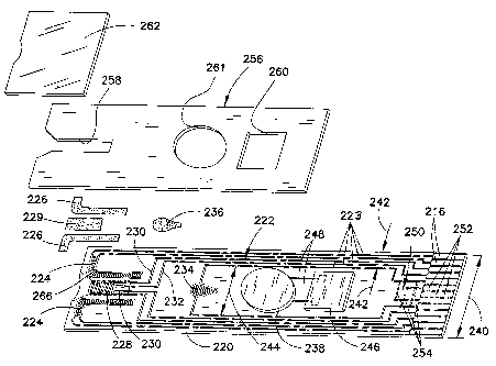
Turning now to Fig. l, strip 200 defines a test strip body that generally
has several zones, including a measurement zone 202, a user interface zone
204, a power generation zone 206, a digital device zone 208 and an instrument
connection zone 210. As indicated in Fig. 1 and as will become clear with the
discussion below, the zones are not limited to specific locations on a given
test
CA 02529579 2005-12-14
WO 2005/012900 PCT/US2004/019652
11
strip 200. Instead, the locations of the various zones will normally overlap
to
varying degrees as shown or may be discontinuous, occupying two or more
different regions of the test strip body. Each zone generally has included
therein electrical devices that perform a specific type or class of function.
For example, the electrical devices included in the measurement zone
typically have functionalities related to the measurement (or correction of
measurement) of the fluid sample being interrogated. Examples of these
electrical devices include macro and micro-electrode sets, dose detection
electrodes, sample sufficiency electrodes, temperature correction or
temperature measurement electrodes, thermistors and the like. While the
measurement zone is illustrated at a dosing end 212 of the strip, it should be
understood that the measurement zone may alternatively occupy other
locations on the strip, e.g., a side of the strip, as is known in the art.
The electrical devices in the user interface zone typically are
electrically driven signal generators which emit a visible, audible or tactile
signal upon occurrence of a "triggering event." As described in more detail
below, the signal generator may be a light that illuminates or turns off after
a
sufficiently sized sample has been received in the measurement zone, the
latter
event being the "triggering event." The user interface zone is in some
embodiments electrically wired to the measurement zone and/or other zones of
the test strip.
The power generation zone includes one or more power generators that
provide power to one or more other electrical devices disposed on or in the
test
strip. Typically, the power generator comprises a battery, but it could also
comprise a capacitor or even a solar cell, depending upon the power
requirements of the electrical device the power generator is going to drive
and
the specific functionality of that device.
Digital devices such as RFID tags, integrated circuits and the like are
disposed within the digital zone and may be wired to the electrical pattern.
In
other embodiments, the electrical pattern that is disposed in the digital zone
is
CA 02529579 2005-12-14
WO 2005/012900 PCT/US2004/019652
12
itself encoded with digital information and thus comprises yet another type of
digital device.
Finally, the instrument connection zone includes electrical devices,
typically contact pads, that electrically link to an instrument (not shown)
which includes driving circuitry and metering circuitry. The driving circuitry
provides a known current and/or potential through contacts 216 and monitors
the current and/or voltage response over a period of time. The metering
circuitry correlates the monitored current, impedance and voltage response to
estimated analyte concentration or other aspect of the analyte. While the
instrument connection zone is preferably disposed on a meter insertion end
214 of the strip, this need not necessarily be the case. The instrument zone
could be located on a side of the strip or could be located on the end as
shown,
but could also include contact pads that are disposed at various locations on
the top, bottom or sides of the test strip.
Strip Architecture and Components.
With further reference to Figs. 1 and 2, strip 200 is generally of a
laminar structure and includes three primary layers. The base substrate layer
220 is generally a flexible polymeric material such as polyester, especially
high temperature polyester materials; polyethylene naphthalate (PEN); and
polyimide, or mixtures of two or more of these. A particularly preferred base
substrate material is a 10 mil thick MELINEX~ 329 layer available from
duPont. Substrate 220 is initially coated with a conductive material such as a
50 nm layer of gold, and the complex electrical pattern 222 can be then
formed therefrom by broad field laser ablation. The broad field laser ablation
method is described in the METHOD OF MAKING A BIOSENSOR
application incorporated above. Materials for the specific biosensor layers
and
the method of assembling those materials is described in the Slot Vent
Opening application, also incorporated above.
The electrical pattern 222 includes contacts or contact pads 216, which,
as described above, can be electrically linked to an instrument that reads
strip
CA 02529579 2005-12-14
WO 2005/012900 PCT/US2004/019652
13
200. Traces 223 run lengthwise along strip 200 and are typically used to
connect electrical devices to the contact pads 216 or to connect two or more
electrical devices on or in strip 200 together. For example, substrate 220
includes a measuring electrode set 228 coated by a reagent 229 and a sample
sufficiency electrode set 230, the operation of which are described in detail
in
the Dose Sufficiency, Slot Vent Opening, and DEVICES AND METHODS
RELATING TO ELECTROCHEMICAL BIOSENSORS applications, all of
which were incorporated by reference above. These electrode sets are
connected to their respective contact pads by traces 230 and 232 and in turn
through traces 223 as shown.
User interface devices comprising L-shaped micro-electrode arrays
224 are formed on base substrate 220 and are coated with organic light
emitting diodes ("OLEDs") 226, which illuminate upon a voltage being
provided across arrays 224. The voltage is applied or removed upon or after
the occurrence of a triggering event, as described in more detail below.
Similarly, micro-electrode set 234 formed on substrate 220 is coated with a
second OLED 236 that illuminates or turns off upon the occurrence of the
same or a different triggering event, as is also described in more detail
below.
A power generator 238 is provided on strip 200 and can be used to
power various other electrical devices present on the strip, as explained
below.
Many suitable power generators are commercially available and can be
employed as power generator 238, but power generator 238 should preferably
be formed as a small and especially thin material so as not to significantly
increase the thickness of test strip 200.
Test strip 200 includes digital device 246, which is shown in Fig. 2
wired to power generator 238 by traces 248. Digital device 246 may be an
integrated circuit, an RFID tag or other digital device, as described in more
detail below. Further, a portion of the electrical pattern may comprise a
digital
device 250, as explained in more detail below.
Laminated to base substrate 220 is a spacer layer 256, formed, e.g.,
from a 4 or 5 mil thick Melinex~ 329, 339 or 453 material available from
CA 02529579 2005-12-14
WO 2005/012900 PCT/US2004/019652
14
DuPont Teijin Films. In certain embodiments, particularly those including
light emitters such as OLEDs 226 and 236, it is preferable that the spacer
layer
material be clear or translucent so that the OLEDs are visible when lit. The
Melinex~ 453 material works well for this purpose. Spacer layer 256 forms a
void 258 that defines the height and perimeter of the sample receiving
chamber 218 (Fig. 1). The precise volume of the sample receiving chamber is
defined in the Slot Vent Opening application, which was incorporated above.
Spacer layer 256 also includes "cut-outs" 260 and 261 that are sized to
receive
digital device 246 and power generator 238, respectively. These devices will
typically be thicker than the spacer layer, such that they may protrude
slightly
from the top of strip 200 as shown in Fig. 1.
A covering layer 262 overlies and is laminated to spacer layer 256.
Covering layer 262 is also preferably made from a transparent Melinex~ film
that is about 4-5 mils thick. Covering layer 262 overlies most of void 258 and
forms the ceiling or top boundary for sample receiving camber 218. The cover
terminates short of the full length of void 258 and thereby forms a vent
opening 264 as shown. Vent 264 allows air to be displaced from chamber 218
as fluid sample enters it. As can be appreciated with respect to Fig. 1, OLED
coatings 226 and 236 are visible when lit through the covering and spacer
layers.
Optionally, to reduce the extent to which devices 238 and 246 protrude
from strip 200, cover layer 262 may extend further toward meter insertion end
214, such that it is coextensive with layer 256. The cover 262 would then be
formed with a hole overlying the void 258 to form the vent. Alternatively, the
cover could be formed in two pieces forming a gap therebetween, as described
in the Slot Vent Opening application, incorporated by reference above. This
longer spacer layer may also include cut-outs that align with cutouts 260 and
261 and reduce the extent to which devices 238 and 246 protrude from strip
200. Typically, however, it is preferable for electrical devices in the user
interface or power generation zones to be sufficiently thin such that they can
CA 02529579 2005-12-14
WO 2005/012900 PCT/US2004/019652
be covered by covering layer 262 for protection from electromagnetic
interference.
Electrical Pattern.
5 The electrical patterns for use with embodiments incorporating the
present invention are typically formed by broad field laser ablation, which is
described in detail in the METHOD OF MAKING A BIOSENSOR
application that was incorporated by reference above. This method allows
several electrical functionalities to be located within and outside of
10 measurement zone 202 -- with room to spare on an already very small test
strip. For example, arrow 240 in Fig. 2 represents the approximate width of
strip 200, which is about 9 mm in the illustrated embodiment. The strip
illustrated in Figs. 1 and 2 is preferably about 33 - 38 mm in length. Arrows
242 illustrate the distance from the edge of the strip to the innermost trace
223,
15 and this width can be configured to be about 1 mrn or even as small as
about
0.2 mm. Remarkably, this means that width 244, which is the width available
for components such as power generator 238 and digital device 246, can be
about 8 mm or more for a 9 mm wide strip having ten electrical traces running
lengthwise along it. One of ordinary skill should readily appreciate that the
electrical patterns embodied by the present invention, while complex, can
nonetheless be advantageously configured into a relatively small space, such
that ample room remains for other devices having relatively large footprints
to
be placed on the strip.
Measurement Zone.
Generally, the measurement zone incorporating the present invention
can vary widely insofar as the type and quantity of functionalities provided
therein. Turning to Figs. 1 and 2, the measurement zone 202 includes a sample
receiving chamber 218 whose periphery is approximately indicated in Fig. 2
by dashed line 266. (As indicated above, the precise volume of the sample
receiving chambers of various embodiments disclosed in this application can
CA 02529579 2005-12-14
WO 2005/012900 PCT/US2004/019652
16
be determined with reference to the Slot Vent Opening application,
incorporated by reference above.) Macro-electrode array 228 includes a
working electrode and a counter electrode, each having one or more
interdigitated fingers as shown. Electrode set 228 estimates the concentration
of analyte based upon the reaction of the analyte with the reagent 229 coated
on the electrode set. Once a sufficient sample has entered chamber 218, a
suitable potential or series of potentials across the working and counter
electrodes are applied, and the impedance or other characteristic is measured
and correlated to the concentration of analyte. Measuring electrodes of this
type and reagent suitable for reagent layer 229 are described in the Slot Vent
Opening and DEVICES AND METHODS RELATING TO
ELECTROCHEMICAL BIOSENSORS applications incorporated above, and
need not be described in further detail herein.
As mentioned, the voltage or potential is preferably not applied across
electrode set 228 until the sample chamber has filled with the requisite
volume
of sample. In this connection, sample sufficiency electrode set 230 is
provided
at a downstream location in chamber 218. When fluid has wetted electrode set
230, its resistance or impedance (which can be intermittently monitored by
applying a voltage to the contact pads 216 connected to electrode set 230)
will
drop, thereby indicating sample has reached the interior end of the chamber
and sufficient sample has thus been received. A potential or series of
potentials can thereafter be driven across electrode set 228 to perform the
measurement. Sample sufficiency electrodes suitable for use with the present
invention are disclosed in the Dose Sufficiency application that was
incorporated by reference above. Additionally, once the sample sufficiency
electrodes indicate that sufficient sample has been received, they can be used
for other measurements, as also disclosed in the Dose Sufficiency application.
It should also be understood that a single sample sufficiency electrode could
be used and a voltage applied across it and one of the measurement electrodes
for testing.
CA 02529579 2005-12-14
WO 2005/012900 PCT/US2004/019652
17
Turning now to Fig. 3, a test strip 300 is shown with a sample
receiving chamber having multiple, redundant functionalities. Strip 300
includes base substrate 302, four sets of micro-electrodes 304, 306, 308 and
310, and a set of sample sufficiency electrodes 312 formed thereon. A reagent
layer whose edges are indicated by dashed lines 314 and 316 is coated onto the
micro-electrode sets. Strip 300 also includes a spacing layer 318 having a
void section 320, which, in cooperation with covering layer 322 and base
substrate 302, partially defines the boundaries of the sample receiving
chamber. The position of the sample receiving chamber is generally indicated
by dashed line 324 on substrate 302, although the void portion beneath the
vent is not part of the sample receiving chamber. The micro-electrode sets and
sample sufficiency electrodes are electrically connected to contact pads 326
through traces 328. The architecture just described is essentially the same as
that described with reference to Figs. 1-2, the difference being the
electrical
devices contained in the sample receiving chamber. Advantageously, a large
central portion 330 of the base substrate 302 is not occupied by the
electrical
pattern and would be available to add additional user interface, power, or
digital devices, as described elsewhere herein.
In the embodiment shown in Fig. 3, identical microelectrodes are
provided to make identical measurements. Sample fluid enters the sample
receiving chamber 324 and is drawn in by capillary action past each of the
micro-electrode arrays until it wets sample sufficiency electrode set 312,
whereupon potentials are applied across each of the microelectrode arrays 304,
306, 308 and 310. The circuitry in the instrument (not shown) that reads the
strips drives a potential across each electrode set through contacts 326 and
traces 328. Alternatively, electrodes sets 304, 306, 308 and 310 could be
wired
in parallel (not shown), in which case a single pair of contact pads would
connect all four electrode sets to the meter. In this case, the parallel
configuration of the four sets would provide an "on strip" average for the
value being measured by the four electrode sets.
CA 02529579 2005-12-14
WO 2005/012900 PCT/US2004/019652
18
Even though it contains five electrode sets, sample receiving chamber
324 nonetheless has a very small volume, on the order of less than about 500
n1.
Turning now to Fig. 4, a test strip 400 is shown having a measurement
zone with multiple, different functionalities. Strip 400 includes base
substrate
402 with four sets of electrodes 404, 406, 408 and 410, and a set of fault
detect
electrode traces 412 and 413 formed thereon. A reagent stripe 414 is coated
onto electrode set 404 and micro-electrode set 406 in this embodiment. Strip
400 also includes a spacing layer 418 having a void section 420, which, in
cooperation with covering layer 422 and base substrate 402, defines the
boundaries of the sample receiving chamber. The position of the sample
receiving chamber is indicated generally by dashed line 424 on substrate 402.
The electrode sets and sample sufficiency electrodes are electrically
connected
to contact pads 426 through traces 428. The architecture just described is
essentially the same as that described with reference to Fig. 2, the
difference
being the electrical devices contained in the measurement zone. Again, a large
central portion 430 of the base substrate 402 is not occupied by the
electrical
pattern and would be available to add additional user interface, power, or
digital devices, as described elsewhere herein.
In the embodiment shown in Fig. 4, The first electrode pair 404
encountered by the sample includes working electrode 432, a single-finger
electrode. First electrode pair 404 also includes counter electrode pair 434,
a
two-finger electrode, with one finger on either side of working electrode 432.
Each finger in first electrode pair 434 is about 250 ~m wide, and a gap of
about 250 ~.m separates each counter electrode finger from the working
electrode finger. The system driver connects to contacts 426 to use the first
electrode pair 404 to obtain an estimated concentration of analyte in the
sample.
The second electrode pair 406 comprises two electrodes of five fingers
each. These fingers are each about 50 ~,m wide with a separation of about 30
~m between them. Each electrode in the second pair connects to a conductive
CA 02529579 2005-12-14
WO 2005/012900 PCT/US2004/019652
19
trace 428 to be electrically connected to a contact 426, which contacts are
used
to drive and measure for a first correction factor such as hematocrit based on
the analyte interaction with the second pair of electrodes.
The third electrode pair 408 is also a micro-electrode configuration,
with each of the two electrodes in the third pair 408 having five fingers
interdigitated with the five in the other electrode. Each finger is again
about
50 ~,m wide, with a gap of about 30 ~,m between them. Each electrode in the
third pair 408 is connected via a conductive trace 428 to a contact 426, which
contacts are used to drive and measure for a second correction factor such as
temperature based on the analyte interaction with the second pair of
electrodes.
The fourth set of electrodes comprises sample sufficiency electrodes
410 that signal when the sample has filled the chamber such that electrode
sets
404, 406 and 408 can then be driven to perform their respective measurement
functions.
The fifth functionality in the measurement zone of strip 400 relates to
fault detect traces 412 and 413 for electrode set 404. Trace 413 connects to
counter electrode 434 and is used to correct variant voltage across the pair,
whereas fault detect trace 412 on working electrode 432 compensates for
measured current. Additionally, traces 412 and 413 can be used to apply a
potential between the primary traces and the fault detect traces to determine
whether there are any defects in the primary traces. This fault detection
feature is fully described in the Quality Assurance application that was
incorporated by reference above.
Even with five electrical devices or functionalities provided in the
measurement zone, the sample receiving chamber 424 nonetheless has a very
small volume, on the order of less than about 500 n1.
Turning now to Fig. 5, a base substrate 502 for a test strip of the type
described above is shown. Substrate 502 includes an electrical pattern 504
formed thereon having contact pads 506 and traces 508 leading to the
electrode sets disposed in the measurement zone 510. Measurement zone 510
CA 02529579 2005-12-14
WO 2005/012900 PCT/US2004/019652
includes a sample receiving chamber 512 having three branches or prongs 514,
516 and 518. Branch 514 includes electrode sets 520 and 522, branch 516
includes electrode sets 524 and 526, and branch 518 includes electrode sets
528 and 530. A reagent layer 532 covers electrode sets 520 and 522, a reagent
5 layer 534 covers electrode sets 524 and 526, and a reagent layer 536 covers
electrode set 528 and 530. A spacing layer (not shown in Fig. 5) as described
above is formed with voids corresponding to and defining the branched
sample receiving chamber, and a covering layer overlies the spacing layer.
Vent holes are formed in the covering layer to allow air to escape each of the
10 branches of the sample receiving chamber.
One advantage of the system shown in Fig. 5 is that it allows multiple
analytes to be tested in a single test strip. For example, reagent layers 532,
534 and 536 can be comprised of three different reagents for testing three
different analytes, e.g., a lipid panel that tests total cholesterol, HDL
15 cholesterol and triglycerides. Reagents with appropriate enzymes and
mediators for these analytes are disclosed in the Reagent Stripes application
that was incorporated by reference above. Alternatively, all three reagents
can
be identical, in which case three of the same tests can be performed in
parallel,
such that each branch of the sample receiving chamber effectively receives its
20 own fresh supply of fluid sample. By contrast, a series of electrode sets
in a
single-branched chamber poses the potential of contamination to the
downstream electrode sets.
As with the embodiments illustrated above, it should be appreciated
that a large portion 538 is available in the middle of substrate 502 and could
be configured to support additional electrical devices.
Power Generation
Returning now to Figs. 1 and 2, a power generator.238 is positioned
centrally on strip 200. The power generator 238 may comprise a battery such
as a commercially available custom made Power Paper brand energy cell,
available from Power Paper, Ltd., Kibbutz, Israel. These cells are preferably
CA 02529579 2005-12-14
WO 2005/012900 PCT/US2004/019652
21
printed on a very thin substrate such as paper or thin polymer. By means of
basic screen-printing techniques, different layers of conductive inks are
printed to form the various components of cell 238, which are then laminated
together and in turn laminated to substrate 220. In the embodiment illustrated
in Fig. 2, battery 238 has a diameter of about 5.3 mm and a thickness of less
than about 0.5 mm. Battery 238 is mounted to substrate 220 by ordinary
adhesives or other suitable means and connects to leads 248 as show,
preferably by conductive epoxy. Battery 238 produces 2.7 - 3.1 Volts, a
current of 4 - 5 mA and has an "on time" of between 5-90 seconds. These
parameters are sufficient for powering one of the inventive OLED circuits
described below, a traditional LED, or a small piezoelectric device which
produces sound, or any number of similar devices. In view of the teachings
herein, which minimize the footprint of even complex electrode patterns, two
or more such batteries 238 could be positioned on strip 200 and wired together
to increase power production.
Other power generators 238 could be substituted for the battery just
described. For example, if only a short burst of energy is needed, for example
to light a diode or produce a short audible sound, a super capacitor or ultra-
cap
modified to have a very slim profile could be used as power generator 238. In
use, for example, in one embodiment, strip 200 would be inserted into the
instrument (not shown) for strip identification, strip integrity checks,
temperature determination, and charging the capacitor or other power storage
element. The self-powered strip is then removed from the instrument, placed
at the dose site, and returned to the instrument for measurement computation
and display.
In view of the teachings herein, one of skill in the art would readily
recognize other power generators that could be employed as power generator
238. It is preferable, however, that the power generator be as thin as
possible
so as not to significantly increase the thickness of the test strip.
CA 02529579 2005-12-14
WO 2005/012900 PCT/US2004/019652
22
Digital Devices.
Still referring to Figs. 1 and 2, a digital device 246 is positioned
adjacent power generator 238 and is wired thereto by traces 248. Device 246
could be a radio frequency identification ("RF)D") tag. RFID 246 is preferably
less than about lmm thick, more preferably less than 0.5 mm thick, and has a
width of less than about 7 mm. In one embodiment, device 246 contains
digital calibration data concerning the test strip and can communicate such
data to an RFID reader (not shown) that is included in the instrument (not
shown). Most commercially available RFID's are typically "passive," i.e.,
they are powered by the radio signal emanating from the reader that reads
them. Thus, if device 246 is an RF>D, it need not be wired to a power
generator such as power generator 238. RFC technology is known in the art
and the details thereof need not be described any further herein.
As noted above, digital device 246 could be provided as an on-board
integrated circuit with computing power, powered by battery 238 and
connected thereto by traces 248. Two commercially available examples
include Texas Instruments MSP430C11 and Microchip PIC12F675 integrated
low power micro-controllers for governing sample acquisition and
rudimentary measurements to support dosing the strip without the strip being
inserted in the meter. As yet another option, device 246 could be provided in
the form of a conventional wired storage device such as a Microchip 24AA01
1I~ bit serial EEPROM, in which event it would include data such as lot code,
calibration data and the like.
As shown in Fig. 2, strip 200 also includes a digital device 250 which
is comprised of a combination of contact pads 252 and conductive links 254 of
electrical pattern 222. Contact pads 252 and conductive links 254 are shown
in phantom because any one (or all) of them may or may not be present in the
finished test strip, depending upon the information that is to be encoded onto
the test strip. Each link or contact pad can be thought of as a binary switch
having a value of 0 (if not present) or 1 (if present). Any given
configuration
of absent/present links and contact pads may include digital information
CA 02529579 2005-12-14
WO 2005/012900 PCT/US2004/019652
23
concerning lot code, expiration date, type of analyte the strip is intended to
analyze and so forth. A detailed enabling description of digital device 250 is
disclosed in an application entitled the Coding Information application that
was incorporated by reference above.
Optionally, a photodiode sensor could be mounted on the test strip in
the digital device zone or elsewhere to detect an environmental condition such
as ambient light. The meter could then apply a voltage to the micro-electrode
arrays such as micro-electrode arrays 224 so that they illuminate the
measurement zone. One of skill in the art should thus appreciate that the term
"digital device" for purposes of this application is somewhat broader than its
common usage in the art, in that it includes devices such as a photodiode or
similar devices that may be provided in the digital zone.
User Interface Devices.
As briefly described earlier, the test strip 200 shown in Figs. 1 and 2
includes a user interface zone 204 that includes OLEDs coated onto micro-
electrode arrays. Specifically, with reference to Fig. 2, OLEDs 226 are coated
onto micro-electrodes 224 and OLED 236 is coated onto micro-electrode array
234.
Electrode arrays 224 are wired through traces 223 to contact pads 216.
Thus, a "triggering event" occurs when strip 200 is inserted into a meter (not
shown), upon which event the circuitry of the meter recognizes that a strip
has
been inserted and produces a voltage across electrode sets 224. In turn, the
coatings 226 illuminate. If the strip 200 is being used in conditions of dim
lighting, the OLED coating advantageously illuminates the sample receiving
chamber 218 so that the user can visually confirm that the fluid sample is
contacting the correct part of the strip 200 and that the sample fluid is
being
drawn into the strip. As noted above, the spacer and covering layers forming
test strip 200 are preferably transparent or translucent such that the light
emitted from the OLEDs is visible through them.
CA 02529579 2005-12-14
WO 2005/012900 PCT/US2004/019652
24
OLED 236 can be configured to illuminate (or turn off) upon sufficient
sample being received in the sample receiving chamber. Sample sufficiency
electrodes 230 are wired through traces 223 to contact pads 216 and in turn to
the meter (not shown) that reads the strips. Once the meter detects from
electrodes 230 that the chamber is filled with the requisite size sample, the
meter can apply a voltage across electrode set 234 through the appropriate
contact pads 216 and traces 223. OLED 236 will then illuminate, thereby
providing the user a positive visual indication that the chamber has been
properly filled.
Fig. 6 shows a base substrate 600 of another test strip embodiment
incorporated by the present invention. The test strip has a measurement zone
602, two user interface zones 604 and 604', a power generation zone 606, and
a meter connection zone 610. This embodiment illustrates the point alluded to
above, viz., that the locations of various "zones" of a particular test strip
embodying the principles of the present invention may overlap, or in the case
of the embodiment illustrated in Fig. 6, may be discontinuous or bifurcated.
The sample receiving chamber 612 includes three different electrical
devices or functionalities: a measurement electrode set 614, a thermistor 616
and a sample sufficiency electrode set 618. Electrode set 614 is connected to
traces 620, which terminate in contact pads 622 disposed at meter connection
zone 610 of the strip.
The sample sufficiency electrode set 618 is part of a circuit which
includes a micro-electrode array 624 having an OLED 626 coated thereon and
a battery 628. Electrical devices 618, 624 and 628 are wired in series by
traces
630, 632 and 634. Traces 630 and 634 terminate in the power generation zone
606 with contact pads 636 (shown in phantom) to which the battery 628 is
connected. The second or bifurcated user interface zone 604' includes a
traditional diode 638 wired by traces 620 to contact pads 622.
In use, the strip is dosed with a sample that is drawn into chamber 612
by capillary action. In the embodiments described above, the sample
sufficiency electrodes were adapted to be driven by circuitry from a meter to
CA 02529579 2005-12-14
WO 2005/012900 PCT/US2004/019652
which the strip is inserted. The embodiment in Fig. 6, however, employs a
different approach. In this embodiment, sample sufficiency electrode set 618
acts as a switch in the circuit containing electrodes 618, electrode array 624
and battery 628. Battery 628 is a Power Paper type battery as described above
5 that produces 2.7 - 3.1 Volts and a current of 4 - 5 mA for about 5-90
seconds.
Once the aqueous fluid sample saturates sample sufficiency electrodes 618,
the circuit closes. If blood is the sample fluid, the ionic strength thereof
should be sufficient to close the circuit. However, one skilled in the art
would
readily recognize numerous coatings that could be applied and dried onto
10 electrode set 618 to ensure sufficient current transfer upon wetting with
other
fluid samples. In any event, closing the circuit is a triggering event which
results in a voltage being produced across micro-electrode array 624, which in
turn causes OLED layer 626 to illuminate. In this manner, the illumination of
OLED 626 provides a positive visual verification to the user that the sample
15 chamber has been filled.
Electrical device 616 is a thermistor that is used to measure the
temperature of the sample receiving chamber. One thermistor suitable for
device 616 is surface mount thermistor available from Vishay Intertechnology,
Inc., Lavern, PA, part no. NTHS-0402NO1N100KJ. Thermistor 618 is driven
20 by electrical circuitry from a meter (not shown) through contacts 622 and
traces 620. If the temperature of the sample receiving chamber is not within a
desired range for testing, the meter circuitry can apply a voltage to
conventional LED 638 through contacts 622 and traces 620 to cause it to
illuminate. This signals the user that the temperature of the sample is
outside
25 of a preferred range, in which event the user may then possibly repeat the
test
under better conditions. An LED that is suitable for mounting on substrate
600 is available from Stanley Electrical Sales of America, Inc., part no.
PY1114CK. This LED is mounted to base substrate 600 preferably by a
conductive epoxy. Optionally, instead of an LED, user interface zone 604'
may include a signal producing device that produces sound, such as a
CA 02529579 2005-12-14
WO 2005/012900 PCT/US2004/019652
26
piezoelectric available from U.S. Electronics, Inc., St. Louis MO., part
number
USE14240ST.
Turning now to Fig. 7, a test strip with yet another innovative
electrically driven signal generator is illustrated. Base substrate 700 of the
test
strip includes a measurement zone that includes a sample fluid receiving
chamber 702 having disposed at least partially therein a measurement
electrode set 704 and sample sufficiency electrode set 706, whose
functionality and operation are described above. Suitable spacing and
covering layers (not illustrated in Fig. 7) cover substrate 700 to form a test
strip, as described above and in the Slot Vent Opening application
incorporated by reference above. Substrate 700 includes a numerical display
712 comprised of individual segments 714 that have a shape not unlike that of
the segments used for traditional LED or LCD displays. The layer or layers of
the test strip (not shown) that cover display 712 are translucent or
transparent
such that display 712 is visible therethrough. Segments 714 include an OLED
coating like that described above overlying a micro-electrode IDA, as also
described above (but not shown in Fig. 7). Each segment 714 has two
electrodes (not shown) having two traces 708 extending therefrom and leading
to respective contact pads 710. Voltages can be applied across selective ones
of the contact pads 710 to illuminate display 712 to produce any of the digits
0
to 9, a "5" being shown illuminated in Fig. 7.
Optionally, additional digits and associated contact pads and traces can
be provided with display 712 on substrate 700. The design of the test strip
with this numerical display should balance (1) the desire to keep the strips
small, (2) the need to make the display large enough to be read by even those
users with impaired vision, and (3) the space required from substrate 700 to
accommodate the traces, contact pads, and digits. A test strip having a base
substrate 700 as shown in Fig. 7 with one digit has a length of about 33-
38mm, a width of less than about 15 mm, preferably about 9rnm, and a
thickness of less than about 1 mm. The other layers that are laminated to
substrate 700 can be configured and assembled in accordance with the Slot
CA 02529579 2005-12-14
WO 2005/012900 PCT/US2004/019652
27
Vent Opening application, incorporated by reference above. It should be
appreciated that the micro-electrode arrays and OLEDs coating them (to form
segments 714 of display 712) do not increase the thickness of the strip.
In use, the test strip having substrate 700 is inserted into a meter (not
shown), a fluid sample is provided to sample receiving chamber 702, and the
meter calculates the numerical estimate of analyte concentration. Thereupon,
the circuitry in the meter drives voltages across selective ones of the
contact
pads 710 to illuminate a number on display 712 that corresponds to the
estimate of analyte concentration. If only one digit were provided in display
712 as shown in Fig. 7, and the analyte whose concentration is being estimated
were glucose from a blood sample, the single digits could be assigned a range.
For example, a "0" might correspond to a 50-100 mg/dl concentration of
glucose, a "1" to 100-150 mgldl, a 2 to 150-200 mgldl and so on. If two digits
were provided in display 712, then the display could simply show the first two
digits of the result. In such case a "10" displayed would mean 100-109 mg/dl,
a "21" would mean 210-219 mg/dl, etc.
Alternatively, the analyte concentration might be displayed by
sequentially displaying digits. For example, "126" mg/dL might be displayed
as a "1" followed by a "2", followed by a "6", and the sequence terminated
with a unique symbol to indicate completion and avoid user confusion. In this
manner, a three-digit whole number can be conveyed to the user with a single
digit display.
With three digits, a whole number for mg/dl concentration can be
displayed all at once, as is typically done with traditional glucose meters.
While Fig. 7 embodies an electrochemical test strip, it should be
understood that the innovative on-board display could be provided on test
strips which employ other measurement techniques, e.g., photometric
principles.
Forming the test strips or biosensors as flattened articles offers several
advantages, especially in terms of storing and dispensing, as described in the
Dispenser application incorporated above, but it is expected that one skilled
in
CA 02529579 2005-12-14
WO 2005/012900 PCT/US2004/019652
28
the art would apply the teachings herein to other test devices. The inventive
display as well as other features described above may be employed in test
devices other than biosensors, e.g., devices for food testing and other
applications. In such other applications, the devices may have, e.g., a
cylindrical or other than a traditional thin test strip type body. Even
biosensors incorporating the inventive features described herein, while
generally comprising a flat and thin shape, may have portions thereof that are
sized and shaped to accommodate various electrical devices, as described
above.
OLED workin _ e~ples.
Polymer light-emitting devices are typically configured as a thin film
(e.g., about 0.1 microns of a polymer such as polyparaphenylene vinylene)
sandwiched between two different metallic electrodes. The anode is
transparent and lies on a transparent substrate. The typical combination is
indium tin oxide on glass. The experiments below, however, employ a light
emitting polymer coated onto a micro-electrode interdigitated array (IDA) in
which the electrodes are co-planar.
Example I
To preparing the coating, 0.012 g of tris (2,2'-bipyridyl)
dichlororuthenium (II) hexahydrate (CAS Registry No. 50525-27-4 ) was
combined with 1 ml of acetonitrile. The compound did not completely
dissolve. Deionized water was then added dropwise until the ruthenium
compound completely dissolved.
Two functional interdigitated micro-electrode arrays (IDAs) were used.
The IDAs had 750 pairs of interdigitated fingers with each finger having a
width of 2~.m, a length of 6mm, and a spacing between the next closest finger
(i.e., gap width) of about 2 ~Cin. The IDAs were custom fabricated on a
silicon
wafer by Premitec Inc., Raleigh, N.C. The IDAs were each coated with 20,1
of the solution just described. The coated IDAs were then placed in a
CA 02529579 2005-12-14
WO 2005/012900 PCT/US2004/019652
29
desiccator and allowed to dry. The reagent coatings did not dry uniformly
and had a ridge around the circumference of the coating.
Using a BAS 100W electrochemical potentiostat, a 3 volt potential was
applied across the micro-electrode arrays, whereupon light was emitted from
the coatings. Both electrodes were tested several times with light being
emitted from the coating on application of about 3 volts. A Keithley 236
"Source Measure Unit" was than setup as a better voltage source for future
measurements.
Example II
In order to obtain a better coating than that obtained in Example I, a
solution of 1°7o PVP 25k (BASF) was prepared in deionized water. The
ruthenium compound used in Example I was then mixed with the PVP
solution in a 1:1 ratio and the resulting solution was applied to several
additional ll~As. The first IDA had a spacing between the interdigitated
fingers of approximately 2,um as described above and the other had a finger
spacing of approximately 21~,m and 50 finger pairs. This second IDA had a
finger width of 21~,rn, a finger length of 6 mm and was formed on a Upilex
substrate also custom fabricated by Premitec. The coating composition
containing the PVP produced a uniform coating on both types of IDA's.
Using the Keithley SMU-236, a three (3) volt potential was applied
across the IDA with the 21 ,um finger spacing, but this voltage was not
sufficient to cause the OLED to illuminate. Three (3) volts was also applied
across the IDA with the 2 ~,m finger spacing, which caused the OLED to
illuminate with good intensity. Increasing the voltage on the 2 ~,m IDA
increased the intensity. Voltages of about 10-20V were required to produce
reasonable intensities in the ll~A with the 21 ~,m gap width between the
fingers.
CA 02529579 2005-12-14
WO 2005/012900 PCT/US2004/019652
Example III
The electrodes used in the preceding examples were left at room
temperature and humidity and the experiments described above repeated at
approximately 1 - 2 month intervals. The OLEDs still illuminated with the
5 same voltages used in the previous examples.
Other OLEDs.
It is anticipated that substituting other polymers in the OLED matrix
used in the experiments above may improve the results, in terms of the voltage
10 required to illuminate and the overall intensity achieved with a given
voltage.
One such compound is Poly(styrenesulfonate)/poly(2,3-dihydrothieno(3,4b) -
1,4-dioxin), available from Aldrich. Other Poly(sodium, 4-styrenesulfonate)
compounds may also perform well or better than the polymer used in the
above examples. One of skill in the art would recognize that many other
15 known light emitting compounds may work suitable as OLEDs for use in the
biosensors disclosed herein.
While a preferred embodiment incorporating the principles of the
present invention has been disclosed hereinabove, the present invention is not
limited to the disclosed embodiments. Instead, as noted above, this
20 application is intended to cover any variations, uses, or adaptations of
the
invention using its general principles. Further, this application is intended
to
cover such departures from the present disclosure as come within known or
customary practice in the art to which this invention pertains and which fall
within the limits of the appended claims.