Note: Descriptions are shown in the official language in which they were submitted.
CA 02529661 2005-12-15
WO 2005/055275 PCT/US2004/020558
NOVEL SUPERCONDUCT1NG ARTICLES, AND METHODS FOR FORMING AND USING SAME
TECHNICAL FIELD
The present invention is generally directed to superconducting or
superconductor components, and in
particular, a novel superconducting tape, power components incorporating same,
and methods for utilizing and
manufacturing same.
BACKGROUND ART
Superconductor materials have long been known and understood by the technical
community. Low-
temperature (low-T~) superconductors exhibiting superconductive properties at
temperatures requiring use of
liquid helium (4.2K), have been known since about 1911. However, it was not
until somewhat recently that
oxide-based high-temperature (high-T~) superconductors have been discovered.
Around 1986, a first high-
temperature superconductor (HTS), having superconductive properties at a
temperature above that of liquid
nitrogen (77K) was discovered, namely YBaZCu30~_X (YBCO), followed by
development of additional
materials over the past 15 years including Bi2Sr2Ca2Cu301o+y (BSCCO), and
others. The development of high-
T~ superconductors has brought potential, economically feasible development of
superconductor components
incorporating such materials, due partly to the cost of operating such
superconductors with liquid nitrogen,
rather than the comparatively more expensive cryogenic infrastructure based on
liquid helium.
Of the myriad of potential applications, the industry has sought to develop
use of such materials in the
power industry, including applications for power generation, transmission,
distribution, and storage. In this
regard, it is estimated that the native resistance of copper-based commercial
power components is responsible
for quite significant losses in elecixicity, and accordingly, the power
industry stands to gain significant
efficiencies based upon utilization of high-temperature superconductors in
power components such as
transmission and distribution power cables, generators, transformers, and
fault current interrupters. In
addition, other benefits of high-temperature superconductors in the power
industry include an increase in one
to two orders of magnitude of power-handling capacity, significant reduction
in the size (i.e., footprint) of
electric power equipment, reduced environmental impact, greater safety, and
increased capacity over
conventional technology. While such potential benefits of high-temperature
superconductors remain quite
compelling, numerous technical challenges continue to exist in the production
and commercialization of high-
temperature superconductors on a large scale.
Among the many challenges associated with the commercialization of high-
temperature
superconductors, many exist around the fabrication of a superconducting tape
that can be utilized for formation
of various power components. A first generation of HTS tapes includes use of
the above-mentioned BSCCO
high-temperature superconductor. This material is generally provided in the
form of discrete filaments, which
are embedded in a matrix of noble metal, typically silver. Although such
conductors may be made in extended
lengths needed for implementation into the power industry (such as on the
order of kilometers), due to
materials and manufacturing costs, such tapes do not represent a commercially
feasible product.
CA 02529661 2005-12-15
WO 2005/055275 PCT/US2004/020558
Accordingly, a great deal of interest has been generated in the so-called
second-generation HTS tapes
that have superior commercial viability. These tapes typically rely on a
layered structure, generally including
a flexible substrate that provides mechanical support, at least one buffer
layer overlying the substrate, the
buffer layer optionally containing multiple films, an HTS layer overlying the
buffer film, and an electrical
stabilizer layer overlying the superconductor layer, typically formed of at
least a noble metal. However, to
date, numerous engineering and manufacturing challenges remain prior to full
commercialization of such
second generation-tapes.
Accordingly, in view of the foregoing, various needs continue to exist in the
art of superconductors, and
in particular, provision of commercially viable superconducting tapes, methods
for forming same, and power
components utilizing such superconducting tapes.
DISCLOSURE OF INVENTION
According to a first aspect of the present invention, a superconducting
article is provided, which
includes a substrate, a buffer layer overlying the substrate, a superconductor
layer overlying the buffer layer,
and an electroplated stabilizer layer overlying the superconductor layer.
According to a particular feature, the
stabilizer layer may be formed principally of non-noble metals, such as
copper, aluminum, and alloys and
mixtures thereof. A noble metal cap layer may be provided between the
stabilizer layer and the
superconductor layer. The electroplated stabilizer layer may overlie one of
the two opposite major surfaces of
the substrate, both major surfaces, or may completely encapsulate the
substrate, buffer layer, and
superconductor layer. The article may be in the form of a relatively high
aspect ratio tape.
According to another aspect of the present invention, a method for forming a
superconducting tape is
provided, which includes providing a substrate, depositing a buffer layer
overlying the substrate, and
depositing a superconductor layer overlying the buffer layer. Further, an
electroplating step is carried out to
deposit a stabilizer layer overlying the superconductor layer.
According to another aspect of the present invention, a power cable is
provided including a plurality of
superconductive tapes, the superconductive tapes being provided in accordance
with the first aspect of the
present invention described above.
According to yet another aspect of the present invention, a power transformer
is provided including
primary and secondary windings, at least one of the windings including a wound
coil of superconductive tape
provided in accordance with the first aspect of the present invention.
According to yet another aspect of the present invention, a power generator is
provided including a
shaft coupled to a rotor that contains electromagnets comprising rotor coils,
and a stator comprising a
conductive winding surrounding the rotor. The rotor coils and/or the
conductive winding include a
superconductive tape generally in accordance with the first aspect of the
present invention described above.
CA 02529661 2005-12-15
WO 2005/055275 PCT/US2004/020558
According to yet another aspect of the present invention a power grid is
provided, which includes
multiple components for generation, transmission and distribution of
electrical power. Namely, the power grid
includes a power generation station including a power generator, a
transmission substation including a
plurality of power transformers for receiving powex from the power generation
station and stepping-up voltage
for transmission, and a plurality of power transmission cables for
transmitting power from the transmission
substation. Distribution of the power is provided by utilization of a power
substation for receiving power from
the power transmission cables, the power substation containing a plurality of
power transformers for stepping-
down voltage for distribution, and a plurality of power distribution cables
for distributing power to end users.
According to a particular feature of this aspect of the present invention, at
least one of the power grid elements
described above includes a plurality of superconductive tapes, provided in
accordance with the first aspect of
the present invention described above.
Still further, another aspect of the present invention provides a method for
laying power cable,
sometimes also referred to generically as "pulling" cable. The method calls
for providing a coil of power
cable, and unwinding the coil while inserting the power cable into a conduit,
wherein the conduit is an
underground utility conduit. The structure of the power cable is described
above, namely, includes a plurality
of superconductive tapes in accordance with the first aspect of the present
invention.
BRIEF DESCRIPTION OF THE DRAWINGS
The present invention may be better understood, and its numerous objects,
features, and advantages
made apparent to those skilled in the ark by referencing the accompanying
drawings.
FIG. 1 illustrates an HTS conductive tape according to an embodiment of the
present invention.
FIG. 2 illustrates a cross-section of a HTS tape according to another
embodiment of the present
invention in which the entire superconductive tape is encapsulated by
electroplated stabilizer.
FIG. 3 a cross-section of a dual-sided HTS conductive tape according to
another embodiment of the
present invention.
FIG. 4 illustrates an electroplating process according to an embodiment of the
present invention.
FIG. 5 illustrates the results of a current overloading test.
FIG. 6 illustrates the results of testing conducted to evaluate the effect of
overloading on the critical
current of the HTS tape.
FIGS. 7 and 8 illustrate power cables incorporating superconductive tapes.
FIG. 9 illustrates a power-transformer according to an aspect of the present
invention.
FIG. 10 illustrates a power generator according to an aspect of the present
invention
CA 02529661 2005-12-15
WO 2005/055275 PCT/US2004/020558
FIG. 11 illustrates a power grid according to another aspect of the present
invention.
The use of the same reference symbols in different drawings indicates similar
or identical items.
MODES FOR CARRYING OUT THE INVENTION
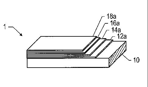
Turning to FIG.1, the general layered structure of an HTS conductor according
to an embodiment of the
present invention is depicted. The HTS conductor includes a substrate 10, a
buffer layer 12a overlying the
substrate 10, an HTS layer 14a, followed by a capping layer 16a, typically a
noble metal layer, and a stabilizer
layer 18a, typically a non-noble metal.
The substrate 10 is generally metal-based, and typically, an alloy of at least
two metallic elements.
Particularly suitable substrate materials include nickel-based metal alloys
such as the known Inconel~ group
of alloys. The Inconel~ alloys tend to have desirable thermal, chemical and
mechanical properties, including
coefficient of expansion, thermal conductivity, Curie temperature, tensile
strength, yield strength, and
elongation. These metals are generally commercially available in the form of
spooled tapes, particularly
suitable for HTS tape fabrication, which typically will utilize reel-to-reel
tape handling.
The substrate 10 is typically in a tape-like configuration, having a high
aspect ratio. For example, the
width of the tape is generally on the order of about 0.4 -10 cm, and the
length of the tape is typically at least
about 100m, most typically greater than about SOOm. Indeed, embodiments of the
present invention provide
for superconducting tapes that include substrate 10 having a length on the
order of lkm or above.
Accordingly, the substrate may have an aspect ratio which is fairly high, on
the order of not less than 103, or
even not less than 104. Certain embodiments are longer, having an aspect ratio
of 105 and higher. As used
herein, the term 'aspect ratio' is used to denote the ratio of the length of
the substrate or tape to the next
longest dimension, the width of the substrate or tape.
In one embodiment, the substrate is treated so as to have desirable surface
properties for subsequent
deposition of the constituent layers of the HTS tape. For example, the surface
may be lightly polished to a
desired flatness and surface roughness. Additionally, the substrate may be
treated to be biaxially textured as is
understood in the art, such as by the known RABiTS (roll assisted biaxially
textured substrate) technique.
Turning to the buffer layer 12a, the buffer layer may be a single layer, or
more commonly, be made up
of several films. Most typically, the buffer layer includes a biaxially
textured film, having a crystalline texture
that is generally aligned along crystal axes both in-plane and out-of plane of
the film. Such biaxial texturing
may be accomplished by IBAD. As is understood in the art, IBAD is acronym that
stands for ion beam
assisted deposition, a technique that may be advantageously utilized to form a
suitably textured buffer layer for
subsequent formation of an HTS layer having desirable crystallographic
orientation for superior
superconducting properties. Magnesium oxide is a typical material of choice
for the IBAD filin, and may be
on the order or 50 to 500 Angstroms, such as 50 to 200 Angstroms. Generally,
the IBAD film has a rock-salt
like crystal structure, as defined and described in US Patent 6,190,752,
incorporated herein by reference.
CA 02529661 2005-12-15
WO 2005/055275 PCT/US2004/020558
The buffer layer may include additional films, such as a barrier film provided
to directly contact and be
placed in between an IBAD film and the substrate. In this regard, the barrier
filin may advantageously be
formed of an oxide, such as yttria, and functions to isolate the substrate
from the IBAD film. A barrier film
may also be formed of non-oxides such as silicon nitride and silicon carbide.
Suitable techniques for
deposition of a barrier film include chemical vapor deposition and physical
vapor deposition including
sputtering. Typical thicknesses of the barrier film may be within a range of
about 100-200 angstroms. Still
further, the buffer layer may also, include an epitaxially grown film, formed
over the IBAD film. In this
context, the epitaxially grown film is effective to increase the thickness of
the IBAD film, and may desirably
be made principally of the same material utilized for the IBAD layer such as
MgO.
In embodiments utilizing an Mg0-based IBAD filin and/or epitaxial film, a
lattice mismatch between
the Mg0 material and the material of the superconductor layer exists.
Accordingly, the buffer layer may
further include another buffer film, this one in particular implemented to
reduce a mismatch in lattice constants
between the HTS layer and the underlying IBAD film and/or epitaxial filin.
This buffer film may be formed of
materials such as YSZ (yttria-stabilized zirconia) strontium ruthenate,
lanthanum manganate, and generally,
perovskite-structured ceramic materials. The buffer film may be deposited by
various physical vapor
deposition techniques.
While the foregoing has principally focused on implementation of a biaxially
textured filin in the buffer
stack (layer) by a texturing process such as 1BAD, alternatively, the
substrate surface itself may be biaxially
textured. In this case, the buffer layer is generally epitaxially grown on the
textured substrate so as to preserve
biaxial texturing in the buffer layer. One process for forming a biaxially
textured substrate is the process
known in the ark as RABiTS (roll assisted biaxially textured substrates),
generally understood in the art.
The high-temperature superconductor (HTS) layer 14a is typically chosen from
any of the high-
temperature superconducting materials that exhibit superconducting properties
above the temperature of liquid
nitrogen, 77K. Such materials may include, for example, YBaZCu30~_X,
BiZSr2Ca2Cu301o+y,
TiZBaZCaZCu3Olo.,.y, and HgBaz CaZCu3 O8+y. One class of materials includes
REBa2Cu30~_X, wherein RE is a
rare earth element. Of the foregoing, YBazCu30~_X, also generally referred to
as YBCO, may be
advantageously utilized. The HTS layer 14a may be formed by any one of various
techniques, including thick
and thin film forming techniques. Preferably, a thin film physical vapor
deposition technique such as pulsed
laser deposition (PLD) can be used for a high deposition rates, or a chemical
vapor deposition technique can
be used for lower cost and larger surface area treatment. Typically, the HTS
layer has a thickness on the order
of about 1 to about 30 microns, most typically about 2 to about 20 microns,
such as about 2 to about 10
microns, in order to get desirable amperage ratings associated with the HTS
layer 14a.
The capping layer 16a and the stabilizer layer 18a are generally implemented
for electrical stabilization,
to aid in prevention of HTS burnout in practical use. More particularly,
layers 16a and 18a aid in continued
flow of electrical charges along the HTS conductor in cases where cooling
fails or the critical current density is
exceeded, and the HTS layer moves from the superconducting state and becomes
resistive. Typically, a noble
metal is utilized for capping layer 16a to prevent unwanted interaction
between the stabilizer layers) and the
CA 02529661 2005-12-15
WO 2005/055275 PCT/US2004/020558
HTS layer 14a. Typical noble metals include gold, silver, platinum, and
palladium. Silver is typically used
due to its cost and general accessibility. The capping layer 16a is typically
made to be thick enough to prevent
unwanted diffusion of the components from the stabilizer layer 18a into the
HTS layer 14a, but is made to be
generally thin for cost reasons (raw material and processing costs). Typical
thicknesses of the capping layer
16a range within about 0.1 to about 10.0 microns, such as 0.5 to about 5.0
microns. Various techniques may
be used for deposition of the capping layer 16a, including physical vapor
deposition, such as DC magnetron
sputtering.
According to a particular feature of an embodiment of the present invention, a
stabilizer layer 18a is ,
incorporated, to overlie the superconductor layer 14a, and in particular,
overlie and directly contact the
capping layer 16a in the particular embodiment shown in FIG. 1. The stabilizer
layer 18a functions as a
protection/shunt layer to enhance stability against harsh environmental
conditions and superconductivity
quench. The layer is generally dense and thermally and electrically
conductive, and functions to bypass
electrical current in case of failure in the superconducting layer.
Conventionally, such layers have been
formed by laminating a pre-formed copper strip onto the superconducting tape,
by using an intermediary
bonding material such as a solder or flux. Other techniques have focused on
physical vapor deposition,
typically, sputtering. However, such application techniques are costly, and
not particularly economically
feasible for large-scale production operations. According to a particular
feature of the embodiment, the
stabilizer layer 18 is formed by electroplating. According to this technique,
electroplating can be used to
quickly build-up a thick layer of material on the superconducting tape, and it
is a relatively low cost process
that can effectively produce dense layers of thermally and electrically
conductive metals. According to one
feature, the stabilizer layer is deposited without the use of or reliance upon
and without the use of an
intermediate bonding layer, such as a solder layer (including fluxes) that
have a melting point less than about
300°C.
Electroplating (also known as electrodeposition) is generally performed by
immersing the
superconductive tape in a solution containing ions of the metal to be
deposited. The surface of the tape is
connected to an external power supply and current is passed through the
surface into the solution, causing a
reaction of metal ions (M~-) with electrons (e ) to form a metal (M).
M~-+ze'=M
The capping layer 16a functions as a seed layer for deposition of copper
thereon. In the particular case
of electroplating of stabilizer metals, the superconductive tape is generally
immersed in a solution containing
cupric ions, such as in a copper sulfate solution. Electrical contact is made
to the capping layer 16a and
current is passed such that the reaction Cu2++2e -j Cu occurs at the surface
of the capping layer 16a. The
capping layer 16a functions as the cathode in the solution, such that the
metal ions are reduced to Cu metal
atoms and deposited on the tape. On the other hand, a copper-containing anode
is placed in the solution, at
which an oxidation reaction occurs such that copper ions go into solution for
reduction and deposition at the
cathode.
CA 02529661 2005-12-15
WO 2005/055275 PCT/US2004/020558
In the absence of any secondary reactions, the current delivered to the
conductive surface during
electroplating is directly proportional to the quantity of metal deposited
(Faraday's Law of Electrolysis).
Using this relationship, the mass, and lience thickness of the deposited
material forming stabilizer layer 18a
can be readily controlled.
While the foregoing generally references copper, it is noted that other
metals, including aluminum,
silver, gold, and other thermally and electrically conductive metals may also
be utilized. However, it is
generally desirable to utilize a non-noble metal to reduce overall materials
cost for forming the
superconductive tape.
While the foregoing description and FIG. 1 describe electroplating to form a
stabilizer layer 18a along
one side of the superconductive tape, it is also noted that the opposite,
major side of the superconductive tape
may also be coated, and indeed, the entirety of the structure can be coated so
as to be encapsulated. In this
regard, attention is drawn to FIG. 2.
FIG. 2 is a cross-sectional diagram illustrating another embodiment of the
present invention, in which
the entire superconductive tape is encapsulated with first stabilizer layer
18a, second stabilizer layer 18b
disposed on an opposite major surface of the superconductive tape, the first
and second stabilizer layers 18a,
18b, joining together along the side surfaces of the superconductive tape,
forming generally convex side
portions or side bridges 20a and 20b. This particular structure is desirable
to further improve current flow and
further protect the HTS layer 14a, in the case of cryogenic failure,
superconductivity quench, etc. By
essentially doubling the cross-sectional area of the deposited stabilizer
layer by forming first and second
stabilizer layers 18a and 18b, a marked improvement in current-carrying
capability is provided. Electrical
continuity between stabilizer layers 18a and 18b ma.y be provided by the
lateral bridging portions 20a and 20b.
In this regard, the lateral bridging portions 20a anel 20b may desirably have
a positive radius of curvature so as
to form generally convex surfaces, which may fixrther reduce build up of
electrical charge at high voltages that
HTS electric power devices will experience. Additionally, to the extent that a
suitably electrically conductive
material is utilized for the substrate 10, further current-carrying capability
can be provided by encapsulation as
illustrated in FIG.2. That is, the bridging portions extending laterally and
defining side surfaces of the tape
may provide electrical connection to the substrate itself, which can add to
the current carrying capability of the
coated conductor (tape).
While not shown in FIG. 2, it may be generally desirable to deposit a noble
metal layer along the
entirety of the superconductive tape, particularly along the side surfaces of
the superconductive tape, to isolate
the superconductor layer 14a from the material of the bridging portions 20a
and 20b, which may be a non-
noble metal such as copper or aluminum as described above.
FIG. 3 illustrates yet another embodiment of the present invention. The
embodiment is somewhat
similar to that shown in FIG. 2, but essentially forms a double-sided
structure, including first and second
buffer layers 12a and 12b, respectively overlying first and second surfaces l
la and l 1b of the substrate 10.
Further, first and second superconductor layers 14a and 14b are provided,
along with first and second capping
CA 02529661 2005-12-15
WO 2005/055275 PCT/US2004/020558
layers 16a and 16b. This particular structure provides an advantage of further
current-carrying capability by
utilizing both sides of the substrate for coating of the superconductor layers
14a and 14b.
FIG. 4 schematically illustrates an electroplating process according to an
embodiment of the present
invention. Typically, electroplating is carried out in a reel-to-reel process
by feeding a superconductive tape
through an electroplating solution 27 by feeding the tape from feed reel 32
and taking up the tape at take-up
reel 34. The tape is fed through a plurality of rollers 26. The rollers may be
negatively charged so as to impart
a negative charge along the capping layers) and/or the substrate for
electrodeposition of the metal ions
provided in solution. The embodiment shown in FIG. 4 shows two anodes 28 and
30 for double-sided
deposition, although a single anode 28 may be disposed for single-sided
electroplating. As discussed above,
the electroplating solution 27 generally contains metal ions of the desired
species for electrodeposition. In the
particular case of copper, the solution may be a copper sulfate solution
containing copper sulfate and sulfuric
acid, for example. The anodes 28, 30 provide the desired feedstock metal for
electrodeposition, and may be
simply formed of high-purity copper plates. It is noted that while the rollers
26 may be electrically biased so
as to bias the superconductive tape, biasing may take place outside of the
solution bath, to curtail unwanted
deposition of metal on the rollers themselves.
A particular example was created utilizing the electroplating technique
described above. In particular,
samples were subjected to DC magnetron sputtering of silver to form 3 micron-
thick capping layers. Those
samples were placed in a copper-sulfate solution and biased such that the
capping layers formed a cathode, the
anode being a copper plate. Electroplating was carried out to form a copper
layer having a nominal thickness
of about 40 microns. Testing of the samples is described hereinbelow.
Namely, a sample that is lcm wide, 4cm long and with 1.7 micron thick YBCO HTS
layer having a
critical current I~ of about 111 A was subjected to a current load of 326 A,.
The sample was overloaded and
voltage data was gathered as illustrated in FIG. 5. The voltage recorded was
44.4mV at 326 A, which
corresponds to heat dissipation of 3.6 W/cm2 -- lower than the critical heat
flux density in LNZ cooling
condition 5 - 20 W/cm2. This means that this coated conductor with 50 micron
stabilizer may carry a current
higher than 326A in LNZ without experiencing burning out. Without the
stabilizer, the estimated power
dissipation is higher than 62.5 I~W/cm2 at 326 A. The foregoing indicates that
the electroplated stabilizer
layer acted as a robust shunt layer to protect the superconducting film from
burning out during the overloading
event.
Subsequently, the sample was then subjected to a second load, following the
overloading event. As
illustrated in FIG. 6, the curves show the same I~ of about 111 A before and
after overloading. The foregoing
indicates that the HTS tape retained its critical current even after the
overloading.
In order to provide adequate current-carrying capability in the stabilizer
layer, typically the stabilizer
layer has a thickness within a range of about 1 to about 1,000 microns, most
typically within a range of about
10 to about 400 microns, such as about 10 to about 200 microns. Particular
embodiments had a nominal
thickness at about 40 microns and about 5~ microns.
CA 02529661 2005-12-15
WO 2005/055275 PCT/US2004/020558
Moving away from the particular structure of the superconducting tape, FIGS. 7
and 8 illustrate
implementation of a superconducting tape in a commercial power component,
namely a power cable. FIG. 7
illustrates several power cables 42 extending through an underground conduit
40, which may be a plastic or
steel conduit. FIG. 7 also illustrates the ground 41 for clarity. As is shown,
several power cables may be run
through the conduit 40.
Turning to FIG. 8, a particular structure of a power cable is illustrated. In
order to provide cooling to
maintain the superconductive power cable in a superconducting state, liquid
nitrogen is fed through the power
cable through LN2 duct 44. One or a plurality of HTS tapes 46 is/are provided
so as to cover the duct 44. The
tapes may be placed onto the duct 44 in a helical manner, spiraling the tape
about the duct 44. Further
components include a copper shield 48, a dielectric tape 50 for dielectric
separation of the components, a
second HTS tape 52, a copper shield 54 having a plurality of centering wires
56, a second, larger LN2 duct 58,
themlal insulation 60, provided to aid in maintaining a cryogenic state, a
corrugated steel pipe 62 for structural
support, including skid wires 64, and an outer enclosure 66.
FIG. 9 illustrates schematically a power transformer having a central core 76
around which a primary
winding 72 and a secondary winding 74 are provided. It is noted that FIG. 9 is
schematic in nature, and the
actual geometric configuration of the transformer may vary as is well
understood in the art. However, the
transformer includes the basic primary and secondary windings. In this regard,
in the embodiment shown in
FIG. 9, the primary winding has a higher number of coils than the secondary
winding 74, representing a step-
down transformer that reduces voltage of an incoming power signal. In reverse,
provision of a fewer number
of coils in the primary winding relative to the secondary winding provides a
voltage step-up. In this regard,
typically step-up transformers are utilized in power transmission substations
to increase voltage to high
voltages to reduce power losses over long distances, while step-down
transformers are integrated into
distribution substations for later stage distribution of power to end users.
At least one of and preferably both
the primary and secondary windings comprise superconductive tapes in
accordance with the foregoing
description.
Turning to FIG. 10, the basic structure of a generator is provided. The
generator includes a turbine 82
connected to a shaft 84 for rotatably driving a rotor 86. Rotor 86 includes
high-intensity electromagnets,
which are formed of rotor coils that form the desired electromagnetic field
for power generation. The turbine
82, and hence the shaft 84 and the rotor 86 are rotated by action of a flowing
fluid such as water in the case of
a hydroelectric power generator, or steam in the case of nuclear, diesel, or
coal-burning power generators. The
generation of the electromagnetic field generates power in the stator 88,
which comprises at least one
conductive winding. According to a particular feature of the embodiment, at
least one of the rotor coils and
the stator winding comprises a superconductive tape in accordance with
embodiments described above.
Typically, at least the rotor coils include a superconductive tape, which is
effective to reduce hysteresis losses.
Turning to FIG. 11, a basic schematic of a power grid is provided.
Fundamentally, the power grid 110
includes a power plant 90 typically housing a plurality of power generators.
The power plant 90 is electrically
connected and typically co-located with a transmission substation 94. The
transmission substation contains
CA 02529661 2005-12-15
WO 2005/055275 PCT/US2004/020558
generally a bank of step-up power transformers, which are utilized to step-up
voltage of the generated power.
Typically, power is generated at a voltage level on the order of thousands of
volts, and the transmission
substation functions to step-up voltages are on the order of 100,000 to
1,000,000 volts in order to reduce line
losses. Typical transmission distances are on the order of 50 to 1,000 miles,
and power is carried along those
S distances by power transmission cables 96. The power transmission cables 96
are routed to a plurality of
power substations 98 (only one shown in FIG. 10). The power substations
contain generally a bank of step-
down power transformers, to reduce the transmission level voltage from the
relatively high values to
distribution voltages, typically less than about 10, 000 volts. A plurality of
fiwther power substations may also
be located in a grid-like fashion, provided in localized areas for localized
power distribution to end users.
10 However, for simplicity, only a single power substation is shown, noting
that downstream power substations
may be provided in series. The distribution level power is then transmitted
along power distribution cables
100 to end users 102, which include commercial end users as well as
residential end users. It is also noted that
individual transformers may be locally provided for individual or groups of
end users. According to a
particular feature, at least one of the generators provided in the power plant
90, the transformers and the
transmission substation, the power transmission cable, the transformers
provided in the power substarion, and
the power distribution cables contain superconductive tapes in accordance with
the present description.
While particular aspects of the present invention have been described herein
with particularity, it is well
understood that those of ordinary skill in the art rnay make modifications
hereto yet still be within the scope of
the present claims.