Note: Descriptions are shown in the official language in which they were submitted.
CA 02530658 2012-06-04
MICROELECTROMECHANICAL MAGNETIC SWITCHES HAVING
ROTORS THAT ROTATE INTO A RECESS IN A SUBSTRATE, AND
METHODS OF OPERATING AND FABRICATING SAME
Field of the Invention
This invention relates to magnetic switches and fabrication methods therefor,
and more particularly to microelectromechanical system (MEMS) magnetic
switches
and fabrication methods therefor.
Background of the Invention
Magnetic switches are used to make or break electrical connections using a
local permanent and/or electro-magnetic field. A "normally open" type of
magnetic
switch closes when brought into close proximity to a suitably oriented
magnetic field,
while a "normally closed" type opens when subjected to a magnetic field. Such
switches may be used in a variety of industrial, medical, and security
applications, and
may be particularly advantageous in situations where opening or closing of a
circuit
may be accomplished without physical contact with the switch. For example, in-
vivo
medical devices may be sealed to provide biocompatibility and to protect the
device.
Such devices may not have an external "on-off' switch to activate the device.
A
magnetic switch sealed within the device and controlled by an external magnet
can
provide a switch to activate the device.
Many commercially available magnetic switches are based on "reed switches"
constructed of thin elastic reeds made of a ferromagnetic material. These
reeds may
be tipped with noble metal films to provide low contact resistance and sealed
into a
1
CA 02530658 2005-12-23
WO 2005/006365
PCT/US2004/018576
glass and/or other tube. When a permanent magnet or electromagnet is brought
into
close proximity with the tube, the reeds either move toward or away from one
another, making or breaking the contact. When the magnet is removed, the reeds
return elastically to their original position, resetting the switch. One
potential
disadvantage of conventional reed-based magnetic switches is that they may be
relatively large, for example about one inch in length and about 1/8" to 1/4"
in
diameter. For applications where small size is desired, such as in-vivo
medical
devices, conventional reed magnetic switches may be too large. Moreover, reed
switches may be undesirably fragile.
MEMS devices have been recently developed as alternatives for conventional
electromechanical devices, in-part because MEMS devices are potentially low
cost,
due to the use of simplified microelectronic fabrication techniques. New
functionality
may also be provided because MEMS devices can be much smaller than
conventional
electromechanical systems and devices. MEMS devices are described, for
example,
in U.S. Patent Application Publication No. 2002/0171909 Al to Wood et al.,
entitled
MEMS Reflectors Having Tail Portions That Extend Inside a Recess and Head
Portions That Extend Outside the Recess and Methods of Forming Same, and U.S.
Patent 6,396,975 to Wood et al., entitled MEMS Optical Cross-Connect Switch.
MEMS devices and manufacturing methods have been used to provide
magnetic switches. For example, Integrated Micromachines Inc. (IMMI) developed
a
reed-like magnetic switch using MEMS technology. See Figure 1. It is a
normally
open switch with approximate dimensions 2.5x2x1 mm and contact resistance in
closed state of about 500,. Unfortunately, the reed configuration may
inherently lead
to poor shock/vibration resistance and/or high contact resistance. It also may
be
difficult to build a normally closed switch based on this technology. The
switch also
may only be configured as Single Pole Single Throw (SPST), but it may be
difficult to
provide Double Pole Single Throw (DPST) or Single Pole Double Throw (SPDT)
versions. Reed switches also generally do not have a wiping action, i.e., they
generally are not self-cleaning and contact resistance may go up with time.
Published U.S. Patent Application Publication No. 2002/0140533 Al to
Miyazaki et al., entitled Method of Producing An Integrated Type Microswitch,
also
describes a MEMS-based microswitch. As described in the Abstract of this
patent
application publication, an integrated type microswitch with high durability
is
provided. The integrated type microswitch is of the construction through micro-
2
CA 02530658 2005-12-23
WO 2005/006365
PCT/US2004/018576
machining process in which a movable plate is provided above a fulcrum means
movable in seesaw movement by means of either electrostatic or magnetic force,
so
that either one of movable contacts mounted on opposite free ends thereof is
on-off
connected to fixed contact disposed in opposite relation due to seesaw
movement of
the movable plate. See the Abstract of this publication.
U.S. Patent 6,320,145 to Tai et al., entitled Fabricating and Using a
Micromachined Magnetostatic Relay or Switch, also describes a MEMS-based
micro switch. As described in the Abstract of this patent, a micromachined
magnetostatic relay or switch includes a springing beam on which a magnetic
actuation plate is formed. The springing beam also includes an electrically
conductive
contact. In the presence of a magnetic field, the magnetic material causes the
springing beam to bend, moving the electrically conductive contact either
toward or
away from another contact, and thus creating either an electrical short-
circuit or an
electrical open-circuit. The switch is fabricated from silicon substrates and
is
particularly useful in forming a MEMs commutation and control circuit for a
miniaturized DC motor. See the Abstract of this patent. A similar
configuration is
described in a publication entitled Microniachined Magnetostatic Switches, to
Tai et
al., Jet Propulsion Laboratory, California Institute of Technology, October
1998, pp. i,
1-7, lb-3b.
A MEMS micromagnetic actuator is also described in U.S. Patent 5,629,918 to
Ho et al., entitled Electromagnetically Actuated Micromachined Flap. As noted
in
the Abstract of this patent, a surface micromachined micromagnetic actuator is
provided with a flap capable of achieving large deflections above 100 microns
using
magnetic force as the actuating force. The flap is coupled by one or more
beams to a
substrate and is cantilevered over the substrate. A Permalloy layer or a
magnetic coil
is disposed on the flap such that when the flap is placed in a magnetic field,
it can be
caused to selectively interact and rotate out of the plane of the magnetic
actuator. The
cantilevered flap is released from the underlying substrate by etching out an
underlying sacrificial layer disposed between the flap and the substrate. The
etched
out and now cantilevered flap is magnetically actuated to maintain it out of
contact
with the substrate while the just etched device is dried in order to obtain
high release
yields. See the Abstract of this patent.
Finally, an implantable medical device that includes a MEMS magnetic switch
is described in U.S. Patent 6,580,947 to Thompson, entitled Magnetic Field
Sensor
3
CA 02530658 2005-12-23
WO 2005/006365
PCT/US2004/018576
for an Implantable Medical Device. As described in the Abstract of this
patent, an
implantable medical device (IMD) uses a solid-state sensor for detecting the
application of an external magnetic field, the sensor comprises one or more
magnetic
field responsive microelectromechanical (MEM) switch fabricated in an IC
coupled to
a switch signal processing circuit of the IC that periodically determines the
state of
each MEM. The MEM switch comprises a moveable contact suspended over a fixed
contact by a suspension member such that the MEM switch contacts are either
normally open or normally closed. A ferromagnetic layer is formed on the
suspension
member, and the suspended contact is attracted or repelled toward or away from
the
fixed contact. The ferromagnetic layer, the characteristics of the suspension
member,
and the spacing of the switch contacts may be tailored to make the switch
contacts
close (or open) in response to a threshold magnetic field strength and/or
polarity. A
plurality of such magnetically actuated MEM switches are provided to cause the
IMD
to change operating mode or a parameter value and to enable or effect
programming
and uplink telemetry functions. See the Abstract of this patent.
Summary of the Invention
Magnetic switches according to some embodiments of the present invention
comprise a substrate including therein a recess. A rotor is provided on the
substrate.
The rotor includes a tail portion that overlies the recess, and a head portion
that
extends on the substrate outside the recess. The rotor comprises ferromagnetic
material, and is configured to rotate the tail in the recess, in response to a
changed
magnetic field, including application of a magnetic field and/or removal of a
magnetic
field. First and second magnetic switch contacts also are provided that are
configured
to make or break electrical connection between one another in response to
rotation of
the tail in the recess, in response to the changed magnetic field. Analogous
methods
of operating a magnetic switch are also provided.
In some embodiments, a hinge is coupled to the rotor, to define an axis about
which the tail is configured to rotate in the recess in response to the
changed magnetic
field. In some embodiments, the recess includes a wall that intersects with
the
substrate at the axis. In some embodiments, the hinge is a torsional hinge
that is
configured to allow the rotor to rotate about the axis. Other conventional
MEMS
hinges also may be provided.
4
CA 02530658 2005-12-23
WO 2005/006365
PCT/US2004/018576
Many configurations of the first and second magnetic switch contacts may be
provided according to various embodiments of the present invention. For
example, in
some embodiments, the first contact is on the head portion and the second
contact is
on the substrate adjacent the head portion. In other embodiments, the first
contact is
on the tail portion and the second contact is in the recess adjacent the tail
portion. In
still other embodiments, a cap is provided on the substrate that is spaced
apart from
the rotor, to allow rotation thereof. In some of these embodiments, the first
contact is
on the head portion, and the second contact is on the cap adjacent the head
portion. In
other embodiments, the first contact is on the tail portion, and the second
contact is on
the cap adjacent the tail portion. Combinations and subcombinations of these
embodiments may be provided.
In still other embodiments of the present invention, the first contact and the
second contact are on the substrate adjacent the head portion. In other
embodiments,
the first contact and the second contact are in the recess adjacent the tail
portion. In
still other embodiments, a cap is provided as described above, and the first
contact
and the second contact are on the cap adjacent the head portion. In still
other
embodiments, the first contact and the second contact are on the cap adjacent
the tail
portion. Combinations and subcombinations of these and/or the previously
described
embodiments may be provided.
In embodiments of the present invention where the first and second contacts
are on the rotor (head portion or tail portion) and the substrate, first and
second vias
maybe provided that extend through the substrate. First and second conductors
also
may be provided that extend through the respective first and second vias. A
respective one of the first and second conductors is electrically connected to
a
respective one of the first and second contacts, to provide external contacts
for the
magnetic switch on the substrate. In other embodiments, where one contact is
provided on the substrate (including on the head or tail portion of the
rotor), and a
second contact is provided on the cap, a via and a first conductor that
extends through
the via may be provided to provide an external contact for the magnetic switch
on the
substrate. Moreover, a second conductor may be provided on the cap that is
electrically connected to the second contact, to provide an external contact
for the
magnetic switch on the cap. In yet other embodiments, when the first and
second
contacts are provided on the cap, first and second electrical conductors also
may be
provided on the cap, a respective one of which is electrically connected to a
respective
5
CA 02530658 2005-12-23
WO 2005/006365
PCT/US2004/018576
one of the first and second contacts, to provide external contacts for the
magnetic
switch on the cap. Accordingly, external contacts for the magnetic switch may
be
provided on the substrate and/or on the cap.
In still other embodiments of the present invention, the first and/or second
contacts are on the substrate outside the head portion, and are configured to
move
beneath the head portion. In some embodiments, the first and/or second
contacts are
configured to inelastically deform, to move beneath the head portion and
remain
beneath the head portion. In some embodiments, first and second beams are
provided
having fixed ends, and movable ends that are connected to the first (or
second)
contact. The first and/or second beams are configured to move, and in some
embodiment to inelastically deform, upon application of heat thereto, to move
the first
(or second) contact beneath the head portion. In still other embodiments, a
beam
having a fixed end and a movable end that is connected to the first (or
second) contact
is provided. The beam is configured to move, and in some embodiments to
inelastically deform, upon application of heat thereto, to move the first (or
second)
contact beneath the head portion. In still other embodiments, an actuator is
provided
on the substrate that is configured to move the first and/or second contacts
beneath the
head portion.
In still other embodiments of the present invention, the rotor is configured
to
rotate the tail in the recess and also to wipe the first and/or second contact
in response
to the changed magnetic field. A contact cleaning or wiping action thereby may
be
provided.
In other embodiments, a permanent magnet also is provided that generates a
constant magnetic field, to maintain the rotor in a predetermined position. In
these
embodiments, the rotor is configured to rotate from the predetermined position
in
response to the changed magnetic field. Moreover, other embodiments can
provide a
latch, such as a snapping tether, that is coupled to the rotor. The latch is
configured to
maintain the rotor such that the first and second contacts continue to make or
break
electrical connection between one another. A bistable switch thereby may be
provided.
In yet other embodiments of the present invention, a housing is provided and a
permanent magnet is coupled to the housing. The magnetic switch is removably
coupled to the housing, and configured such that removal of the magnetic
switch
from the housing causes the first and second magnetic switch contacts to make
or
6
CA 02530658 2012-06-04
break electrical connection between one another. In still other embodiments,
an
electrical device is electrically connected to the first and/or second
contacts, and is
configured to become operative upon the first and second magnetic switch
contacts
making or breaking electrical connection between one another. In still other
embodiments, an encapsulating structure is provided wherein the magnetic
switch and
the electrical device are encapsulated by the encapsulating structure.
Magnetic switches may be fabricated according to some embodiments of the
present invention, by forming on a substrate a rotor comprising ferromagnetic
material and including a tail portion and a head portion at opposite ends
thereof, and a
contact that is outside the rotor. A recess is formed in the substrate beneath
the tail
portion. The contact that is outside the rotor is moved to beneath the rotor.
In some
embodiments, prior to moving the contact, the tail is rotated into the recess
to provide
a gap between the head portion and the substrate. The contact is then moved
along
the substrate into the gap between the head portion and the substrate. In
other
embodiments, the recess may be formed prior to forming the rotor, such that
the tail
portion is formed above the recess.
In some embodiments, the contact is moved by using an external probe. In
other embodiments, a beam is provided on the substrate having a free end that
is
connected to the contact and a fixed end remote from the free end, and the
contact is
moved by deforming the free end of the beam. The beam may be deformed
inelastically using a probe, using heat and/or using an actuator that is also
provided on
the substrate.
Other method embodiments of the present invention place a cap on the
substrate that is spaced apart from the rotor, to allow rotation thereof.
Still other
embodiments form a via that extends through the substrate and form a conductor
that
extends through the via and is electrically connected to the contact, to
provide an
external contact for the magnetic switch on the substrate. Still other
embodiments
electrically connect an electrical device to the contact, and encapsulate the
electrical
device and the substrate. In still other embodiments, the substrate and the
electrical
device that are encapsulated are removably placed into a housing that includes
a
permanent magnet therein, to cause the contact to electrically connect to or
electrically disconnect from the rotor. In still other embodiments, the
substrate and
the
7
CA 02530658 2012-06-04
electrical device that are encapsulated are removed from the housing, to cause
the
contact to electrically disconnect from or electrically connect to the rotor.
According to an aspect, there is provided a magnetic switch comprising:
a substrate including therein a recess;
a rotor that includes a tail portion that overlies the recess and a head
portion
that extends on the substrate outside the recess, the rotor comprising
unmagnetized
ferromagnetic material, being configured to rotate the tail portion in the
recess in
response to a changed magnetic field and the rotor being balanced in relation
to a
torsional hinge used to mount the rotor to the substrate;
first and second magnetic switch contacts that are configured to make or break
electrical connection between one another in response to rotation of the tail
in the
recess in response to the changed magnetic field; and
at least one deformable beam having a fixed end attached to the substrate and
a
movable end extending beneath the head portion to allow for contact with the
head
portion in its rest position and/or to provide the torsional hinge with
mechanical bias.
According to another aspect, there is provided a magnetic switch comprising:
a substrate including therein a recess;
a rotor that includes a tail portion that overlies the recess and a head
portion
that extends on the substrate outside the recess, the head portion and the
tail portion of
the rotor comprising ferromagnetic material and being configured to rotate the
tail in
the recess in response to a changed magnetic field the rotor being balanced in
relation
to a torsional hinge used to mount the rotor to the substrate; and
first and second magnetic switch contacts that are configured to make or break
electrical connection between one another in response to rotation of the tail
in the
recess in response to the changed magnetic field, and at least one deformable
beam
having a fixed end attached to the substrate and a movable end extending
beneath the
head portion to allow for contact with the head portion in its rest position
and/or to
provide the torsional hinge with mechanical bias.
According to another aspect, there is provided a magnetic switch comprising:
a substrate including therein a recess;
7a
CA 02530658 2012-06-04
a rotor connected to the substrate by torsional hinge means for mechanically
biasing the rotor to a first position in relation to the substrate in the
absence of a
magnetic field, the rotor being balanced in relation to the torsional hinge,
the rotor
including a tail portion that overlies the recess and a head portion that
extends on the
substrate outside the recess, the rotor comprising unmagnetized ferromagnetic
material and being configured to rotate the rotor to a second position in
response to a
changed magnetic field, the tail being in the recess when the rotor is in the
second
position; and
first and second magnetic switch contacts that are configured to make or break
electric connection between one another in response to rotation of the tail in
the recess
in response to the changed magnetic field, and at least one deformable beam
having a
fixed end attached to the substrate and a movable end extending beneath the
head
portion to allow for contact with the head portion in its rest position and/or
to provide
the torsional hinge with mechanical bias.
According to another aspect, there is provided a method of fabricating a
magnetic switch comprising:
forming on a substrate, a rotor comprising ferromagnetic material and
including a tail portion and a head portion at opposite ends thereof, and a
contact that
is outside the rotor;
forming a recess in the substrate beneath the tail portion; and
moving the contact that is outside the rotor, to beneath the rotor;
wherein the rotor is configured to rotate the tail portion in response to a
charged magnetic field.
According to another aspect, there is provided a method of operating a
magnetic switch comprising:
rotating a ferromagnetic rotor that includes a tail portion that overlies a
recess
in a substrate and a head portion that extends on the substrate outside the
recess, in
response to a changed magnetic field, such that the tail portion rotates in
the recess
and causes first and second magnetic switch contacts to make or break
electrical
connection between one another.
7b
CA 02530658 2005-12-23
WO 2005/006365
PCT/US2004/018576
Brief Description of the Drawings
Figure 1 illustrates a conventional reed-like magnetic switch using MEMS
technology.
Figures 2-5 are cross-sectional views of magnetic switches according to
various embodiments of the present invention.
Figures 6-9 are top plan views of magnetic switches according to various
embodiments of the present invention.
Figures 10-11 are cross-sectional views of magnetic switches according to
various embodiments of the present invention.
Figures 12A-12B and 13A-13B are top plan views of magnetic switches
according to various embodiments of the present invention.
Figure 14 is a cross-sectional view of a magnetic switch according to various
embodiments of the present invention.
Figure 15 is a conceptual view of an encapsulated magnetic switch in a
removable housing according to various embodiments of the present invention.
Figure 16 is a cross-sectional view of a pop-up structure for an optical
switch
according to U.S. Patent 6,396,975 and U.S. Patent Publication 2002/0171909.
Figures 17A-17B are top plan views of magnetic switches according to
various embodiments of the present invention, during fabrication thereof,
according to
various embodiments of the present invention.
Figures 18A-18B are perspective views of magnetic switches according to
various embodiments of the present invention.
Figure 19A is a top view of a magnetic switch and Figure 19B is a perspective
of a mating cap, according to various embodiments of the present invention.
Figures 20A-20D are cross-sectional views of packaging of magnetic switches
according to various embodiments of the present invention.
Figure 21 is a perspective view of a packaged magnetic switch according to
various embodiments of the present invention.
Figures 22A and 22B are top plan views of magnetic switches according to
other embodiments of the present invention.
Figures 23A and 23B are cross-sectional views of magnetic switches
according to other embodiments of the present invention.
8
CA 02530658 2005-12-23
WO 2005/006365
PCT/US2004/018576
Figure 24A is a top plan view of a magnetic switch according to other
embodiments of the present invention.
Figures 24B and 24C are cross-sectional views taken along the line A-A of
Figure 24A during operation of the switch of Figure 24A.
Figure 25A is a top plan view of a magnetic switch according to other
embodiments of the present invention.
Figures 25B and 25C are cross-sectional views taken along the line A-A of
Figure 25A during operation of the switch of Figure 25A.
Detailed Description
The present invention now will be described more fully hereinafter with
reference to the accompanying drawings, in which embodiments of the invention
are
shown. This invention may, however, be embodied in many different forms and
should not be construed as limited to the embodiments set forth herein.
Rather, these
embodiments are provided so that this disclosure will be thorough and
complete, and
will fully convey the scope of the invention to those skilled in the art. In
the
drawings, the size and relative sizes of layers and regions may be exaggerated
for
clarity. Moreover, each embodiment described and illustrated herein includes
its
complementary conductivity type embodiment as well. Like numbers refer to like
elements throughout.
It will be understood that when an element such as a layer, region or
substrate
is referred to as being "on" another element, it can be directly on the other
element or
intervening elements may also be present. It will be understood that when an
element
is referred to as being "connected" or "coupled" to another element, it can be
directly
connected or coupled to the other element or intervening elements may be
present. In
contrast, when an element is referred to as being "directly on", "directly
connected" or
"directly coupled" to another element, there are no intervening elements
present. It
will also be understood that although the terms first and second are used
herein to
describe various elements, these elements should not be limited by these
terms. These
terms are only used to distinguish one element from another element. Thus, a
first
element could be termed a second element, and similarly, a second element may
be
termed a first element without departing from the teachings of the present
invention.
As used herein, the term "and/or" includes any and all combinations of one or
more of
the associated listed items. It will be understood that if part of an element,
such as a
9
CA 02530658 2005-12-23
WO 2005/006365
PCT/US2004/018576
surface of a conductive line, is referred to as "outer," it is closer to the
outside of the
device than other parts of the element. Furthermore, relative terms such as
"beneath"
or "above" may be used herein to describe a relationship of one layer or
region to
another layer or region relative to a substrate or base layer as illustrated
in the figures.
It will be understood that these terms are intended to encompass different
orientations
of the device in addition to the orientation depicted in the figures.
Figure 2 is a cross-sectional view of a magnetic switch according to various
embodiments of the present invention. As shown in Figure 2, these embodiments
of
magnetic switches include a substrate 200, having a recess 200a therein. The
substrate may comprise a conventional microelectronic substrate, such as a
silicon,
compound semiconductor, semiconductor-on-insulator or other non-semiconductor
substrate that is used to fabricate MEMS devices. In Figure 2, the recess 200a
is
shown as being triangular is cross-section. However, other circular,
elliptical,
ellipsoidal and/or polygonal cross-section shapes may be used. Moreover, in
Figure
2, the recess 200a does not include a separate floor. However, in other
embodiments,
a floor may be provided.
Still referring to Figure 2, a rotor 210 also is provided. Although the rotor
210
is shown as being straight, a curved and/or segmented rotor may be provided.
The
rotor includes a tail portion 210a that overlies the recess 200a, and a head
portion
210b that extends on the substrate 200 outside the recess. The rotor 210
comprises
ferromagnetic material, also referred to as a ferromagnetic rotor. In
particular, the
rotor may be fabricated entirely of ferromagnetic material, or only a portion
thereof
may comprise ferromagnetic material. The rotor 210 is configured to rotate the
tail
210a in the recess 200a in the directions shown by arrows 220 in response to a
changed magnetic field, shown schematically at 230. It will be understood that
the
changed magnetic field may comprise a change in the strength and/or direction
of a
magnetic field, the application of a magnetic field and/or the withdrawal of
the
magnetic field. The magnetic field 230 may be generated by a permanent
magnetic
and/or an electromagnet.
Still referring to Figure 2, first and second magnetic switch contacts 240a
and
240b also are provided. These magnetic switch contacts may be referred to
simply as
"contacts", and are configured to make or break electrical connection between
one
another in response to rotation of the tail 210a in the recess 200a, in
response to the
changed magnetic field 230. It will be understood by those having skill in the
art that
CA 02530658 2005-12-23
a contact may be a separate element, as shown by contact 240b, or may be a
portion
of a larger element, as shown by contact 240a, which comprises a portion of
the head
210b of the rotor 210. Thus, the term ''contact" as used herein encompasses a
separate contact region or a portion of a larger region that functions as a
contact.
Still referring to Figure 2, a hinge (not shown in Figure 2) is coupled to the
rotor 210, to define an axis 250 about which the tail 210a is configured to
rotate in the
recess 200a in response to the changed magnetic field 230. The hinge can
comprise a
torsional hinge and/or other conventional MEMS hinge that allows rotation
about an
axis. In some embodiments, as shown in Figure 2, the recess 210a includes a
wall
200b that intersects with the substrate 200, at the axis 250.
In embodiments of Figure 2, the first contact 240a is on the head portion
210b,
and the second contact 240b is on the substrate 200 adjacent the head portion
210b.
Figure 3 is a cross-sectional view of other embodiments, wherein the first
contact
240a is on the tail portion 210a, and the second contact 240b is in the recess
200a
adjacent the tail portion. Specifically, as shown in Figure 3, the second
contact 240b
is on the wall 200b.
Figure 4 is a cross-sectional view of other embodiments of the present
invention. In Figure 4, a cap 410 also is provided on the substrate 200, and
is spaced
apart from the rotor 210, to allow rotation thereof. In embodiments of Figure
4, the
first contact 240a is on the head portion 210b, and the second contact 240b is
on the
cap 410 adjacent the head portion 21.0b. It will be understood by those having
skill in
the art that the cap 410 may be a single piece cap or multi-piece cap and may
have
various configurations. The cap may act to hermetically seal the device or may
be a
non-hermetic cap.
Figure 5 illustrates other embodiments of the invention, wherein the first
contact 240a is on the tail portion 210a, and the second contact is on the cap
410
adjacent the tail portion.
It also will be understood by those having skill in the art that the various
contact configurations of Figures 2-5 may be combined in various combinations
and
subcombinations. Moreover, depending upon the action of the hinge and the
orientation magnetic field 230, normally open and/or normally closed magnetic
switches may be provided in any of the embodiments of Figures 2-5. Moreover,
in
any of the embodiments of Figures 2-5, external connections for the magnetic
switches may be provided for the first contact by an electrical connection
through the
11
CA 02530658 2005-12-23
WO 2005/006365
PCT/US2004/018576
hinge and/or using other conventional electrical connections, and may be
provided for
the second contact 240b using conductors that are placed on the substrate 200
and/or
on the cap 410, as will be described in detail below.
Figures 6-9 are top plan views of magnetic switches according to other
embodiments of the present invention. In embodiments of Figures 2-5, the first
contact 240a was attached to the rotor 210 and was, therefore, movable,
whereas the
second contact 240b was attached to the substrate 200 or cap 410, and was
fixed. In
contrast, in embodiments of Figures 6-9, both of the contacts are fixed, and
movement
of the rotor electrically connects the contacts to one another or electrically
disconnects
the contacts from one another.
More specifically, in Figure 6, the first contact 240a and the second contact
240b are on the substrate 200 adjacent the head portion 210b. A hinge 252 also
is
illustrated. In Figure 7, the first contact 240a and the second contact 240b
are in the
recess 200a adjacent the tail portion 210a, and, specifically, are on the
recess wall
200b. In Figure 8, the first and second contacts 240a, 240b are on the cap 410
adjacent the head portion 210b. In Figure 9, the first and second contacts
240a, 240b
also are on the cap 410 adjacent the tail portion 210a. It will be understood
by those
having skill in the art that combinations and subcombinations of embodiments
of
Figures 6-9 may be provided, along with combinations and subcombinations of
these
embodiments with embodiments of Figures 2-5, according to various embodiments
of
the present invention.
Figure 10 illustrates other embodiments of the present invention wherein
external contacts are provided for the magnetic switch on the substrate. More
specifically, embodiments of Figure 10 may correspond to Figure 2, except that
Figure 10 also includes first and second vias 1000a, 1000b, that extend
through the
substrate 200. First and second conductors 1010a, 1010b also are provided,
that
extend through the vias 1000a, 1000b. The first conductor 1010a is
electrically
connected to the first contact 240a, for example through the hinge and/or
using other
conventional electrical connections. The second conductor 1010b is
electrically
connected to the second contact 240b. It will be understood by those having
skill in
the art that, in Figure 10, the first and second conductors 1010a, 1010b are
shown as
filling the respective vias 1000a, 1000b. However, in other embodiments, the
first
and second conductors 1010a, 1010b need not fill the entire via 1000a, 1000b.
It also
12
CA 02530658 2005-12-23
WO 2005/006365
PCT/US2004/018576
will be understood that at least one via and at least one conductor may be
provided in
the substrate 200 in embodiments of Figures 3-7.
Figure 11 is a cross-sectional view of other embodiments of the present
invention. Embodiments of Figure 11 may correspond to embodiments of Figure 4,
except that an external contact is provided for the magnetic switch on the cap
410. In
particular, as shown in Figure 11, a conductor 1100 is provided that is
connected to
the second connector 240b, and extends from an inner surface of the cap 410 to
an
outer surface of the cap 410, to provide an external contact for the magnetic
switch on
the cap 410. It will be understood that, in other embodiments, conductor 1110
may
extend through a via in the cap 410 adjacent the second contact 240b. The
conductor
1100 may be formed using conventional screening, plating and/or other
conventional
techniques for selectively metallizing a cap. It also will be understood that
conductors
1100 may be used with embodiments of Figure 5, 8 and/or 9. Moreover,
combinations of embodiments of Figures 10 and 11 may be used to provide
external
contacts for the magnetic switch on the substrate and on the cap. Accordingly,
many
different configurations of external contacts may be provided.
Figures 12A and 12B are top plan views of magnetic switches according to
other embodiments of the present invention. These embodiments may correspond
to
embodiments of Figure 6, but illustrate how the contacts 240a, 240b may be
configured to move during fabrication of the magnetic sensor. In particular,
referring
to Figure 12A, the contacts 240a, 240b may be fabricated from the same layer
as the
rotor 210 and/or the hinges 252, and may thereby be outside the head portion
210b of
the rotor 210. As shown in Figure 12B, forces may be applied in the direction
shown
by arrows 1210a, 1210b, to move the first and/or second contacts 240a, 240b
beneath
the head portion 210b. The forces 1210a, 1210b may be provided by mechanical
probes, by an actuator that is on the substrate 200 and/or using other
techniques. In
some embodiments, the contacts, and/or an element connected thereto, are
configured
to inelastically deform, so that the contacts remain beneath the rotor. It
will be
understood that embodiments of Figures 12A and 12B also may be applied to
embodiments of Figures 2, 3, 6 and/or 7 with respect to the head and/or tail
portions
of the rotor.
As was described above, in some embodiments of Figures 12A and 12B, the
first and/or second contacts are configured to inelastically deform, to move
beneath
the head portion 210b and remain beneath the head portion 210b.
13
CA 02530658 2005-12-23
WO 2005/006365
PCT/US2004/018576
In some embodiments of the invention, the forces 1210a, 1210b may be
provided by actuators that are provided on the substrate 200. Actuators
according to
some embodiments of the present invention may be provided by a thermal arched
beam actuator as described, for example, in U.S. Patent 5,909,078 to Wood et
al.,
entitled Thermal Arched Beam Microelectromechanical Actuators, the disclosure
of
which is hereby incorporated herein by reference in its entirety as if set
forth fully
herein. In other embodiments, an actuator may be provided that uses one or
more
beam members that are responsive to temperature as described, for example, in
U.S.
Patent 6,407,478, entitled Switches and Switching Arrays That Use
Microelectroniechanical Devices Having One or More Beam Menibers That Are
Responsive To Temperature, the disclosure of which is hereby incorporated
herein by
reference in its entirety as if set forth fully herein. As noted in the '478
patent, these
beam members that are responsive to temperature also may be referred to as
"heatuators". Other actuators also may be used.
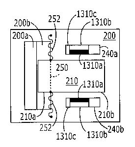
Figures 13A and 13B illustrate embodiments of the invention that may use
heatuators and/or other inelastically deformable beams to move the first
and/or second
contacts from outside the rotor to beneath the rotor. In particular, as shown
in Figure
13A, first and second beams 1310a, 1310b are provided, having fixed ends 1310c
and
movable ends that are connected to the first or second contact 240a, 240b. As
also
shown in Figure 13A, the second beams 1310b are thinner than the first beams
1310a.
Thus, as shown in Figure 13B, upon application of heat such as current through
the
beams, the second beams 1310b inelastically deform to cause the first and
second
contacts to move beneath the rotor in the direction shown by arrows 1210a,
1210b.
The design of heatuator structures are well known to those having skill in the
art and
need not be described further herein. Other deflectable/deformable beam
structures
may be used in other embodiments of the present invention.
Figures 22A and 22B illustrates other embodiments of the invention that may
use heatuators and/or other inelastically deformable beams, to move the
contacts from
outside the rotor to beneath the rotor. In Figure 22A, after current exceeding
a certain
value is applied between the pads 1310c for a short duration while the rotor
210 is
tilted into the trench 200b, the heatuator permanently deforms and the contact
tip
240a slides under the rotor 210.
Figures 23A and 23B are cross-sectional views of magnetic switches
according to other embodiments of the present invention. These embodiments
14
CA 02530658 2005-12-23
WO 2005/006365
PCT/US2004/018576
employ a permanent magnet 2310. Embodiments of Figures 23A and 23B can
provide a normally open switch with a permanent magnetic layer. Normally
closed
switches also may be provided. The permanent magnet 2310 can comprise an
electroplated or screen printed permanent magnet layer and/or other
conventional
permanent magnets. As shown in Figures 23A and 23B, this layer is magnetized
orthogonal to the substrate 200 and generates a constant magnetic field, shown
at 230
in Figure 23A, that maintains the rotor 210 in a predetermined position, shown
as the
open position in Figure 23A.
As shown in Figure 23B, upon application of the changed magnetic field, such
as caused by a second magnet 2320, the rotor 210 is configured to rotate from
the
predetermined position shown in Figure 23 in response to the changed magnetic
field
indicated by 230 in Figure 23B. Thus, in Figure 23B, the switch is closed upon
insertion of the switch in a magnetic field parallel to the substrate 200. In
some
embodiments, this field is stronger than the field from the permanent magnet
2310.
Figures 24A-24C illustrate other embodiments of the present invention,
wherein a latch is provided that is configured to maintain the rotor such that
the first
and second contacts continue to make or break electrical connection between
one
another. A bistable switch may thereby be provided. More specifically, as
shown in
Figure 24A, a latch, which may comprise a snapping or flexible tether 2410,
overlaps
with the rotor 210. As shown in Figures 24B and 24C, as the rotor rotates, the
flexible tethers 2410 bend down and snap above the rotor 210, thereby holding
the
rotor up at a distance from the contact 240a. A horizontal magnetic field can
overcome the tethers 2410, and return the switch to its closed state. Bistable
switches
thereby may be provided.
Figure 14 is a cross-sectional view of other embodiments of the present
invention. Embodiments of Figure 14 may be similar to embodiments of Figure 2,
except embodiments of Figure 14 illustrate that the rotor is configured to
rotate the
tail in the recess and to wipe a contact in response to the changed magnetic
field. In
particular, as shown in Figure 14, upon movement of the rotor 210 clockwise in
the
direction shown by arrow 1410, to hit the contact 240b, the momentum of the
rotor
combined with the flexibility of the hinge can cause the rotor to continue
moving
laterally to the right in Figure 14, and then back to its equilibrium
position, as shown
by arrow 1420, to thereby cause a rubbing or wiping action across the contact
240b.
This wiping action can increase the reliability of magnetic switches according
to some
CA 02530658 2005-12-23
WO 2005/006365
PCT/US2004/018576
embodiments of the present invention. It also will be understood that wiping
action
according to embodiments of the present invention may be provided in any of
the
embodiments described in Figures 1-13B.
Figure 15 is a cross-sectional view of magnetic switches according to other
embodiments of the present invention. As shown in Figure 15, a magnetic
switch,
including a substrate 200 and other elements described above, according to any
of the
embodiments that were described in connection with Figures 1-14, is provided.
A
housing 1520 also is provided including a permanent magnet 1530 that is
coupled to
the housing 1520. The magnetic switch including the substrate 200 is removably
coupled to the housing 1520 and configured such that removal of the magnetic
switch
from the housing 1520, as shown by arrow 1540, causes the first and second
contacts
to electrically connect to and/or electrically disconnect from one another. In
other
embodiments, an electrical device 1550, such as a camera, detector, processor,
storage
device, battery and/or other electrical device is electrically connected to
the magnetic
switch by electrical connection to the first and/or second contacts, and is
configured to
become operative upon a first or second contact electrically connecting to
and/or
electrically disconnecting from one another. In still other embodiments, an
encapsulating structure 1510 may be provided, wherein the substrate 200 and
the
electrical device 1550 are encapsulated by the encapsulating structure 1510.
Accordingly, embodiments of Figure 15 can allow a magnetic switch and an
electrical
device to be encapsulated and activated upon removal of the encapsulated
structure
from the housing 1520.
Figures 2-15 also illustrate methods of fabricating a magnetic switch
according to embodiments of the present invention. According to some
embodiments
of the present invention, a magnetic switch may be fabricated by forming on a
substrate, a rotor comprising ferromagnetic material and including a tail
portion and a
head portion at opposite ends thereof and a contact that is outside the rotor,
as
illustrated, for example, at Figures 12A or 13A. A recess is formed in the
substrate
beneath the tail portion, as also shown in Figures 12A and 13A. In some
embodiments, the recess is fabricated after forming the rotor and/or other
structures.
In other embodiments, the recess is fabricated before forming the rotor, such
that the
tail portion is formed above the recess. Then, the contact(s) that is outside
the rotor is
moved to beneath the rotor as shown, for example, in Figures 12B and 13B. In
some
embodiments, the tail is rotated into the recess, as shown in Figures 2-5, to
provide a
16
CA 02530658 2005-12-23
WO 2005/006365
PCT/US2004/018576
gap between the head portion and the substrate, and then the contact(s) is
moved
along the substrate into the gap between the head portion and the substrate.
In other
methods, a cap may be placed on the substrate as was shown, for example, in
Figures
4, 5, 8, 9 and 11. In still other embodiments, a via is formed that extends
through the
substrate and a conductor is formed that extends through the via, to provide
an
external contact for the magnetic switch on the substrate, as was illustrated,
for
example, in Figure 10. In still other embodiments, as is illustrated in Figure
15, an
electrical device is connected to the contact and the electrical device and
the substrate
are encapsulated. The encapsulated substrate and electrical device are
removably
placed into a housing and, for use, are removed from the housing.
In some embodiments of the present invention, the vias and the conductors
may be fabricated by masking the backside of the substrate according to a
desired via
pattern, and then etching through the substrate from the backside using the
masking.
A KOH etch may be performed. A plating seed layer, such as a Cr/Ni/Ti seed
layer,
may then be formed on the sidewalls of the vias and on the back face of the
substrate,
and the vias may then be filled with a conductor by plating nickel and/or gold
on the
seed layer. The seed layer may then be etched between the vias, lead-tin
solder
bumps may be formed in the vias.
Additional discussion of other embodiments of the present invention now will
be provided. As was described above, magnetic switches according to some
embodiments of the invention can be configured for normally closed and/or
normally
open operations, can have low thresholds of switching magnetic field, can have
high
shock and vibration reliability, and/or low contact resistance. Embodiments of
the
invention can utilize torsional forces acting on a ferromagnetic plate element
tilted in
relation to the magnetic flux lines. Utilizing torsional forces can provide
mass-
balanced design that can have better shock and/or vibration resistance than
comparable reed-like or cantilever-like designs.
As was also described above, in some embodiments, a magnetic switch
includes at least one substrate that can be fabricated from semiconductive
material,
and a ferromagnetic rotor attached to a torsional hinge and/or cantilevers
acting like a
torsional hinge. Two electrically conductive contacts can define open and
closed
states of the switch. In some embodiments, one of the contacts is formed on
the
ferromagnetic rotor. In some embodiments, the second contact is formed on a
contact
arm that is mechanically moved beneath the rotor after tilting it in relation
to the
17
CA 02530658 2005-12-23
WO 2005/006365
PCT/US2004/018576
substrate. In other embodiments, the second contact is formed on a cap that
can
hermetically seal the device, and can provide electrical connections from the
switch
itself to external pad(s) on the other side of the cap. In some embodiments,
the cap
may be used to provide initial tilt to the rotor. In some embodiments,
mechanical bias
of the torsional hinge or cantilevers can determine the contact force and
closed state
resistance of the normally closed configuration. In some embodiments, the
closed
state resistance of the normally open configuration may be determined by an
applied
magnetic field.
As was also described above, other embodiments of the invention can
fabricate a magnetic switch. These embodiments can include forming a torsional
hinge or cantilevers, interconnect lines, hermetic packaging of the switch, a
sacrificial
layer, contact surfaces, and/or a ferromagnetic rotor attached to the
torsional hinge or
cantilevers. In some embodiments, fabrication includes forming a cap from
nonconductive or isolated semiconductive material with conductive vias
providing
electrical interconnects to external pads and a hermetic seal for the moving
components of the switch. In other embodiments, a cap can serve only as a
hermetic
cover and electrical interconnects are formed into the device substrate prior,
parallel
to and/or after the device fabrication.
Some embodiments of the present invention can make use of micromechanical
"pop-up" structures as previously described in U.S. Patent 6,396,975 (Wood et
al.)
and U.S. Patent publication 2002/0171909 Al (Wood), the disclosures of which
are
hereby incorporated herein by reference in their entirety as if set forth
fully herein.
The Wood et al. patent and the Wood patent publication provide optical
switches
based on magnetically actuated 1"pop-up" mirrors to redirect light paths
within the
switch. A plate made of ferromagnetic material such as nickel is fabricated on
the
surface of a silicon wafer and attached to the wafer through a flexible
torsion hinge.
A trench on one side of the hinge allows the "tail" of the plate to rotate
beneath the
plane of the substrate while the "tip" of the plate rotates upward off the
wafer surface.
A voltage can be applied across a first electrode on the tail and a second
electrode on
the trench wall to electrostatically latch the reflector in the up position,
as noted in
Paragraph [0034] of the Wood et al. patent publication. The basic action of
these
devices is shown in Figure 16.
Some embodiments of the invention may arise from recognition that a device
of Figure 16 may be modified to include contacts and contact metallurgy in
order to
18
CA 02530658 2005-12-23
WO 2005/006365
PCT/US2004/018576
produce a magnetic switch, as shown in Figures 17A-17B. In some embodiments of
the invention, as shown in Figure 17A, a rotor plate is provided comprising
one or
more layers of ferromagnetic materials such as electroplated nickel, permalloy
and/or
other magnetic alloys. The rotor is connected to the substrate via an elastic
torsion
hinge, cantilevers and/or other structure comprising silicon nitride, silicon,
polysilicon, silicon oxide and/or similar suitable material. In some
embodiments, as
shown in Figure 17A, to form a switch contact, slender contact arms are co-
fabricated
on both sides or in the center of the rotor tip.
In some embodiments, as shown in Figure 17B, using an automated robotic
assembly process, these contact arms are mechanically bent under the rotor to
allow
contact with the rotor tip in its rest position and/or to provide the hinge
with
mechanical bias for switch closure. To facilitate the arm-bending process, the
rotor
tail is pushed downward, rotating the mirror tip upward and out of the way. A
trench
beneath the rotor tail provides clearance for the rotor tail as it is pushed
down. The
trench edge acts as a fulcrum or axis for rotation of the rotor. The contact
arms
remain in the bent position due to plastic deformation of the nickel. The arms
may be
configured to control the bending action and limit their bending mode to the
substrate
plane. Suitable mechanical "stops" and latches can be employed to limit the
amount
of bending of the contact arms during robotic assembly. Figures 18A-18B are
perspective views of different embodiments of the mechanically microassembled
contact arms, after assembly and during actuation, respectively.
In some embodiments of the invention, restoring force produced by the elastic
hinge brings the bottom surface of the rotor into contact with the upper
surface of the
contact arms. These surfaces may be coated with a noble metal such as gold,
platinum and/or rhodium in order to produce a suitable electrical contact.
Contact
force may be determined through a combination of hinge elasticity, angular
bias of the
rotor at its new rest position, and/or distance of switch arms from the hinge
rotational
axis.
As shown in Figure 18B, in some embodiments, the switch is actuated by
applying a local magnetic field with its flux lines oriented perpendicular to
the
substrate. The field produces torque on the rotor due to the tendency of the
rotor to
orient its long axis with the magnetic lines of force. A rotor that is
perfectly
perpendicular to the field lines may not be compelled to rotate in a
particular
direction, since either clockwise or anticlockwise rotation will align the
mirror to the
19
CA 02530658 2005-12-23
WO 2005/006365
PCT/US2004/018576
field lines. However, because of the placement of the trench and the
counterclockwise rotational bias imposed by the contact arms, the device in
Figure
18B can rotate preferentially in the counterclockwise direction. The rotor
plate may
also be made asymmetrical with respect to the hinge axis, i.e., the section
that rotates
upward can be longer than the section that rotates downward. This can cause
the rotor
to rotate upwardly preferentially. With sufficiently strong field, rotation
takes the
rotor out of contact with the contact arms, interrupting the circuit and
opening the
switch. When the magnetic field is removed, the restoring force produced by
the
hinge brings the rotor back into contact with the contact arms, completing the
circuit
once again.
Embodiments of the present invention can make use of the reluctance effect,
i.e., the torque produced is due to lowest-energy alignment of a ferromagnetic
plate in
a uniform field. Using soft magnetic materials such as Permalloy (80/20 NiFe
alloy)
can make this effect independent of the polarity of magnetic field. In other
embodiments, it is also possible to employ a remnant field effect, i.e., to
permanently
magnetize the plate with a North and South Pole, and/or by electrodepositing
an array
of poles with their fields oriented perpendicular to the substrate. This could
be done,
for example, by electroplating the plate or array of poles in a suitable
magnetic field,
and/or by magnetizing the plate/poles after fabrication. A remnant field rotor
may
produce higher torque that could be exploited to produce a more compact
device,
higher closure force, and/or greater sensitivity to the applied external
magnetic field.
However, devices utilizing remnant field effect may operate only with one
polarity of
magnetic field.
The embodiments of Figures 18A-18B show a "shorting bar" style of switch,
i.e., a broken circuit that is closed at two points of contact by the rotor.
It will be
appreciated by those skilled in the art that other switch types, including
those that use
one point of contact, may be constructed according to other embodiments of the
invention.
Other embodiments of the invention can provide Normally Closed MEMS
Magnetic Switch (NCMS) which can have high contact force provided by a
mechanically biased torsional hinge or cantilevers, which can be
microassembled and
tested on fully automated probe station before packaging, and/or which can be
mechanically biased during packaging. Low contact resistance can be provided
in the
closed state due to the high contact force and use of noble highly conductive
non-
CA 02530658 2005-12-23
WO 2005/006365
PCT/US2004/018576
corrosive metals such as gold, platinum, palladium, and/or rhodium for contact
surfaces. Some embodiments can provide torsional hinges or cantilevers made of
silicon nitride that can be about 10 times stronger than steel and can have
little or no
creep to provide performance over, for example, billions of cycles.
Other embodiments can provide wiping action closure as a self-cleaning
mechanism. The wiping action can come from the complex motion of the rotor
during the closure. First, the rotor turns around the hinge axis. Then, it
hits the contact
point located close to the initial axis of rotation (relative to the rotor
size) and starts
rotating around the contact point. Finally, it comes to the rest position that
is
deteimined by rotor friction at the contact point, hinge torque, and hinge
bending in
planes normal and parallel to the rotor. This motion can result in a desirable
wiping
action. Other embodiments can provide mechanically balanced moving components
and mechanically biased torsional springs to reduce or minimize shock and
vibration
sensitivity and to reduce or eliminate bouncing of the switch after closure.
Embodiments of the invention can be used as a SPST switch, a DPST switch
and/or Multiple Pole- Single Throw configurations. SPDT, DPDT and/or Single
Pole-Multiple Throw configurations also may be provided. Double or multiple
poles
may be provided by arraying single pole configurations, by providing multiple
isolated contacts on a rotor, by providing a split rotor on a common hinge
and/or by
other techniques.
For example, referring to Figures 25A-25C, SPDT or normally open magnetic
switches may be provided, wherein the rotor is divided into two parts 210,
210' that
may be connected by a nitride or other insulating common hinge 252b that does
not
include interconnecting metal. Alternatively, the two rotors 210, 210' can be
mechanically independent and pre-tilted individually. One of the rotors 210
can have
a stiffer outer hinge 252a than the other hinge 252c and can have a contact
flap 240a
under the tail part. The flap can be anchored at 240a' and can be moved down
away
from the other rotor after assembly as shown in Figure 25B. A magnetic field
230 can
turn both rotors up as shown in Figure 25C, but one rotor can go up faster
than other
due to varying stiffness of the outer hinges 252a, 252c. Moreover, a "make
before
break" or "break before make" configuration may be provided, depending on the
relative hinge stiffness. Magnetic sensitivity can be determined by the
difference in
stiffness between the hinges 252a, 252e and/or the difference in size between
the two
rotors 210, 210'.
21
CA 02530658 2005-12-23
WO 2005/006365
PCT/US2004/018576
Inexpensive MEMS processing techniques may be used, and, in some
embodiments, deep Reactive Ion Etching may not be needed. In some embodiments,
performance that can be enhanced or altered by using hard magnetic materials
for the
rotor instead of soft magnetic nickel or permalloy. Finally, magnetic switches
according to embodiments of the invention can be wafer-level chip-scale
heimetically
packaged in a Surface Mount Technology (SMT)-compatible package suitable for
high-volume production.
Normally Open MEMS Magnetic Proximity Switch (NON/TS) also can be
provided according to one or more of the mentioned above embodiments. In some
embodiments, its resistance in the closed state may be determined by magnetic
force
pushing the rotor against the contact located on the cap. Normally Open MEMS
Magnetic Switch (NOMS) also may be provided, which has a ferromagnetic rotor
mass-balanced in relation to weak torsional hinge that can achieve high
magnetic
sensitivity and can achieve good shock and vibration reliability at the same
time.
Magnetic switches according to embodiments of the invention may be used
where a small magnetic switch is desired. Because of its potentially small
package
size and potentially exceptionally low contact resistance, promising
applications for
the normally closed embodiments may be in battery-powered devices that are
activated upon separation from the parent system or a certain object. These
devices
may be very small and/or they could be in a "sleep" mode, without consuming
energy,
for a long time. Implantable or other in-vivo medical devices have been
mentioned
above. Other applications may include underwater devices, space satellites,
structural
monitoring systems utilizing multiple sensors for detection of major cracks or
movements of the structural elements of buildings, bridges, etc. due to
overload or
earthquakes.
In other embodiments, the contact arm may be bent by passing current through
it. This "heatuator" design was described in the US Patent No. 6,407,478.
Embodiments shown in Figure 19 can use plastic deformation resulting from
heating
asymmetric shapes with electric current.
Figure 19A is a top view of magnetic switch layouts according to various
embodiments of the present invention. A rotor 210, a first contact 240a, a
second
contact 240b and trench 200a are shown. The first contact 240a is electrically
connected to a seal ring 1910a on the substrate which can mate with a seal
ring 1910b
on a cap 410. The second contact 240b is electrically connected to a contact
pad
22
CA 02530658 2005-12-23
WO 2005/006365
PCT/US2004/018576
1100a, which can mate with the contact pad 1100b on the cap 410. The cap 410
of
Figure 19B can be mounted on the substrate 210 of Figure 19A. In some
embodiments, the cap 410a of Figure 19B may include one or more through-holes
as
described in U.S. Patent Application Publication No. 2003/0071283, published
April
17, 2003, entitled Semiconductor Structure With One or More Through-Holes.
However, many other configurations of caps may be provided, as was already
described.
Other embodiments of the present invention can make use of existing Chip-
Scale, Chip-on-Flex, and TAB (Tape Automated Bonding) Packaging approaches to
develop non-hermetic packaging of MEMS devices with low I/O count. These
embodiments may be especially suitable for MEMS devices with "pop-up" elements
that can raise about 100-500 m above the silicon level. Some embodiments can
use a
magnetically actuated microelectromechanical magnetic switch as described
above.
Other embodiments can be used to package other MEMS devices.
Embodiments of Figures 18A-18B can provide a Normally-Closed (NC)
MEMS magnetic switch as was described above. A device shown in Figure 10 can
be
about 1.5x2.0 mm in size in some embodiments, and its rotor's upper end can be
as
high as about 200p,m above the surface of the substrate and contact pads.
According
to some embodiments of the invention, it may be packaged in an SMT-compatible
package with maximum footprint of 2x3 mm. There may be two contact pads on the
substrate.
A packaging sequence according to some embodiments of the invention is
described in Figures 20A-20D. As shown in Figure 20A, a Known Good Die (KGD)
is covered by an optional thermally oxidized silicon cap. The cap is picked up
by a
standard vacuum tool, then it touches 1-2 mils thick adhesive, then mounted on
the
chip as shown in Figure 20A. The optional silicon cap is used to protect the
MEMS
chip and to pick it up. An alternative might involve usage of miniature spring-
loaded
suction caps.
As shown in Figure 20B, the MEMS chip is attached to a bottom rigid flex
board by a single drop of adhesive in the center. The bottom board has through-
plated
1/4 or 1/2 vias and may be made by laminating about 16 mils FR4 board to
Kapton
flex. The top surface of the chip should be about 1 mil higher than FR4.
As shown in Figure 20C, a bead or drops of conductive adhesive is deposited
along the edges of the chip on the gold contact pads.
23
CA 02530658 2005-12-23
WO 2005/006365
PCT/US2004/018576
Finally, as shown in Figure 20D, the top board is attached (laminated) on the
top. It includes (top to bottom): copper pads; Kapton or thin FR4 board (if
the
optional silicon cap is not used); thick, 1kFR4 (8-16 mils); copper flex
fingers (similar
to TAB contacts) coated with adhesive on the bottom side; plated through 1/4
vias or
1/2 vias; and copper can be coated by immersion gold.
Figure 21 shows the profile and the top view of the section of a silicon cap
wafer. In Figure 21, the cap is shown as semi-transparent to show the internal
features. Some embodiments may provide a packaged component of 1.6 x 1.6 x
0.8mm. Front-end processes may increase dimensions up to 0.2 mm.
As shown in Figure 21, routing from the MEMS contact points can be made
through the 2-layer L TCC ceramic lid. Soldering/interconnection pad
coplanarity
can be provided by standard LTCC process well below SMD requirements. Both
solder pads have sidewall metallization, so visual solder meniscus can be
visually
inspected as for most SMT components. Component delivery may be on industry
standard tape and reel. The metal sealing ring (200 urn width) assembly
process can
be dry-flux / flux-less. The cavity is dry air or neutral gas filled to
provide both low
dew point and high reliability of MEMS over time. The failure mode may be
c(jet
damage / subsequent sticking. An arc constraining gas may not be needed due to
low
current and voltage conditions along with the number of cycles in operation of
the
switch. MEMS assembly may be done with lid arrays. Dicing / die separation may
occur after the device has been sealed, which can offer the high cleanliness
inside the
device cavity.
In the drawings and specification, there have been disclosed embodiments of
the invention and, although specific terms are employed, they are used in a
generic
and descriptive sense only and not for purposes of limitation, the scope of
the
invention being set forth in the following claims.
24