Note: Descriptions are shown in the official language in which they were submitted.
CA 02532033 2006-O1-10
WO 2005/008849 PCT/US2004/022227
METHOD OF FORMING A SCRIBE LINE
ON A PASSIVE ELECTRONIC COMPONENT SUBSTRATE
Technical Field
[0001] The present invention relates to a method ofi forming a scribe line in
a
passive electronic component substrate, and more particularly to a method of
using an ultraviolet laser to ablate a passive electronic component substrate
and thereby form a scribe line along which the substrate may be broken into
multiple pieces.
Background of the Invention
[0002j As is well known to those of skill in the art, passive and hybrid
microelectronic circuit components (hereinafter circuit "components"), are
fabricated in an array on a ceramic substrate. The ceramic substrate is cut,
sometimes called diced, to singulate the circuit components from one another.
[0003] For the past 30 years, the predominant method of singulating ceramic
substrates involved using a pulsed C02 laser dicing process in which a pulsed
laser was aligned with and then directed along a street to form a "post hole"
scribe line. Fig. 1 is a scanning electron micrograph (SEM) of a post hole
scribe line 2 formed by pulsed C02 laser cutting. As shown in Fig. 1, post
hole
scribe line 2 includes spaced-apart vias 4 that extend into the thickness of a
ceramic substrate 6 along the length of scribe line 2. Following formation of
the
post hole scribe line, force is applied to the ceramic substrate portions on
either
side of the scribe line to effect fracture of the ceramic substrate into
separate
pieces.
CA 02532033 2006-O1-10
WO 2005/008849 PCT/US2004/022227
2
[0004] Although pulsed C02 laser cutting offers advantages in speed,
cleanliness, accuracy, and reduced kerf, the use of the post hole scribe line
creates separate ceramic pieces having jagged and uneven side edges as well
as significant melted slag residue. As shown in the SEM of Fig. 2, ceramic
substrate piece 6 formed in accordance with the post hole scribe line method
has sinusoidal-shaped side edges 8 rather than the preferred straight and
smooth side edges. Further, ceramic substrate piece 6 includes slag residue 7.
[0005] Pulsed C021aser cutting also leads to distortion of the interior
structure of the ceramic surface, resulting in structurally weak components.
Specifically, the strength of the ceramic substrate is reduced, decreasing its
ability to withstand thermal or mechanical stress. The structural weakness of
the interior often evidences itself in an increased number of microcracks
present near the laser scribe line. Figs. 3A and 3B are SEMs showing cross-
sections of ceramic substrate pieces formed using pulsed C02 laser cutting.
Fig. 3A shows a ceramic substrate piece at 10x magnification, and Fig. 3B
shows the side edge of a ceramic substrate piece at 65x magnification. Both
figures show multiple microcracks 9 extending from side edge 8 into the
interior
of the ceramic substrate piece 6. According to Weibull's strength theory, the
flexural strength of the ceramic substrate decreases as the density of
microcracks increases (Weibull, W., Proc. R~y. Sinredish Inst. Engrg.
Research,
193.151 (1939)). Manufacturing costs increased because many of the circuit
components were discarded as a consequence of their insufficient flexural
strength.
[0006] Until recently, fired ceramic substrates had length and width
dimensions of about 6 x 8 inches and a thickness of about 1 mm. The uneven
side edges, slag residue, and microcracks formed as a result of pulsed C02
laser cutting were tolerable when scribing ceramic substrates having these
specifications.
[0007] However, recent technological advances in component
miniaturization necessitate singulation of circuit components having length
and
width dimensions of about 1 mm x 0.5 mm (0402) or 0.5 mm x 0.25 mm (0201 )
and a thickness of between about 80 microns and about 300 microns. Circuit
CA 02532033 2006-O1-10
WO 2005/008849 PCT/US2004/022227
3
components of this density and/or thickness cannot tolerate such uneven side
edges, slag residue, and microcracks resulting from either pulsed COZ or
Nd:YAG laser cutting because these methods of laser cutting adversely affect
the specified circuit component values and/or subsequent component
processing.
[0008] One prior art attempt to singulate these smaller and thinner circuit
components entailed sawing through the ceramic substrate using a saw blade
that had been aligned with a "street" created by the thick and thin film
patterns
formed on the ceramic substrate as part of the process of forming the circuit
components. Alignment of the saw blade and street was achieved using an
alignment system. Tape was preferably attached to the ceramic substrate
before sawing to provide support for the singulated circuit components upon
completion of sawing. Problems with this prior art method include inexact
positioning and alignment of the saw blade, mechanical wobbling of the saw
blade, and uneven or rough surfaces resulting from the mechanical nature of
cutting with a saw blade. Further, the width of the scribe line had to be
sufficiently large to accommodate the width of the saw blade. A typical saw
blade is 75-150 microns wide along its cutting axis, producing cuts that are
about 150 microns wide. Because the resulting scribe lines had relatively
large
widths and therefore occupied a greater portion of substrate surFace, fewer
components could be produced for any given size of ceramic substrate. This
resulted in more wasted surface area, less surface area available for circuit
component parts, and a greater than optimal cost of each circuit component.
[0009] The method by which most large-sized chip resistor components are
formed involves initially precasting the scribe lines into a ceramic substrate
in
an unfired state. The resistor components are then printed on the fired
ceramic
substrate, and the substrate is broken along the scribe lines to form separate
circuit components. Due to normal variations in the positional accuracy of the
precast scribe lines and unpredictable variation in the amount of ceramic
substrate shrinkage during firing, subsequent printing of the resistor
components often results in inadequate alignment with the precast scribe
lines.
CA 02532033 2006-O1-10
WO 2005/008849 PCT/US2004/022227
4
This inadequacy of alignment is indirectly proportional to the size of the
component parts.
[0010] For smaller circuit components, a YAG laser may be used to form the
scribe lines in a fired ceramic substrate. These scribe lines are used to
align
subsequent printing steps. For example, an IR-YAG laser operated at a
wavelength of about 1.O,um can be used to form a scribe line in a ceramic
substrate. The method of forming the scribe line involves imparting relative
motion between the IR-YAG laser beam and each of the top and bottom
surfaces of the ceramic substrate to form trenches in them. When a breakage
force is applied to either side of a trench, cracks propagate into the length
and
thickness of the substrate, resulting in fracture of the ceramic substrate
into
multiple pieces.
[0011] Some drawbacks of using this method include: (1) thermal damage
caused by use of an IR-YAG laser results in de-lamination of the metal
conductor pads; (2) misalignment of the top and bottom surface scribe lines
resulting in non-uniform side margins of the diced ceramic substrate pieces;
and (3) inefficiency resulting from the necessary flipping, realigning, and
sequential scribing of the top and bottom surfaces and consequent
consumption of more than twice the time required to scribe a single surface.
[0012] One of the popular scribing methods used in the past has been to
first pre-scribe the fired chip resistor ceramic substrates and then align the
screen printing of the conductor patterns and resistor patterns to the scribe
lines. However, as circuit component size further decreases, aligning the
screen printing patterns to the previously formed scribe lines becomes very
difficult to accomplish.
[0013] It consequently became necessary to form off axis scribe lines in the
printed and fired finished chip resistor pattern. This need was also evident
for
ceramic components (chip capacitors, conductors, filters, etc.) that had been
fired, a process that entails exposing the ceramic substrate to temperatures
of
between about 750° C and about 1100° C. Prolonged exposure to
these high
temperatures causes the ceramic substrates to warp along one or both axis,
resulting in the formation of a non-standard shaped ceramic substrate. Thus, a
CA 02532033 2006-O1-10
WO 2005/008849 PCT/US2004/022227
need arose for a laser that could align with and accurately scribe these
nonstandard-shaped ceramic substrates to form multiple nominally identical
circuit components. Those skilled in the art will understand that the printing
and
scribing sequence can be interchanged without affecting the end result.
[0014] Additionally, many circuit components have a top layer that includes
metal. This layer can extend into either or both of the streets extending
along
the x-axis or the y-axis. Those of ordinary skill will readily recognize that
the
existence of metal in the top layer prevents the use of a C02 laser since the
metal reflects the C02 laser beam. Further, mechanically sawing a metal-
containing layer is undesirable because the ductile nature of many metals,
such
as copper, make mechanical sawing of a metal-containing layer an extremely
slow and difficult process.
[0015] Via drilling using an UV-YAG laser has been used extensively in the
printed wiring board (PWB) industry. Specifically, a UV-YAG laser emits a
laser
beam that cuts through the top, metal-containing layer before the underlying
organic material is drilled. Thus UV laser drilling of copper, and other
metals
used in the fabrication of circuit components, is well understood by those of
ordinary skill in the art.
[0016] What is needed, therefore, is an economical method of forming in a
substrate made of ceramic or ceramic-like material a scribe line that
facilitates
the clean fracture of the substrate into separate circuit component parts
having
clearly defined side margins, minimal slag residue, and a reduced incidence of
microcracking.
Summary of the Invention
[0017] An object of the present invention is, therefore, to provide a method
by which a passive electronic component substrate, onto which has been
affixed multiple evenly-spaced electronic components, may be cleanly
singulated into separate circuit components, including, e.g. resistors,
capacitors, inductors, filters, varistors, and thermistors.
[0018] The method of the present invention entails directing a UV laser
beam to form a scribe line along a passive electronic component substrate such
that a portion of the thickness of the substrate is removed to form a trench.
The
CA 02532033 2006-O1-10
WO 2005/008849 PCT/US2004/022227
6
trench has a width that converges from the substrate surface to the bottom of
the trench to define a sharp snap line.
[0019] The term "passive electronic component substrate" is used herein to
refer to a single layer structure and consolidated stack, multi-layer, and
laminated multi-layer structures. Passive electronic component substrates are
of different types including, but not limited to, preferred ceramic or ceramic-
like
materials described below.
[0020] A first type is a ceramic substrate constructed in either single layer
or
multi-layer plate form. The scribe lines can be formed in green (soft) or
fired
(hard) plates, including high temperature co-fired ceramic (HTCC) and low
temperature co-fired ceramic (LTCC) materials.
[0021] A second type is a single layer fired ceramic substrate patterned with
individual (chip) resistors, resistor networks, or hybrid resistor networks
(i.e.,
those having more than one sheet resistivity value); piezoelectric, electro-
optic,
or opto-electronic devices; inductors; or other individual components built on
the larger multi-element ceramic substrate.
[0022] A third type is implemented with multi-layer ceramic technology,
including, for either HTCC or LTCC materials, chip capacitors, chip arrays,
networks composed of arrays of multiple component types (e.g., resistors,
capacitors, and inductors), and HTCC and LTCC electronic packages
containing passive components or electronic packages for use as interposers
connecting semiconductor (e.g., silicon) devices to other electronic packages.
[0023] A fourth type is a specialized ceramic substrate, either fired or
unfired, and of either single layer or multi-layer construction, such as, for
example, a substrate of a varistor or a thermistor. Single layer construction
of
thermistor and varistor substrates is referred by skilled persons to any one
of
discs, rods, washers, slabs, plates, tubular shapes, and beads.
[0024] The UV laser emits a laser beam characterized by an energy and
spot size sufficient to form a scribe line in the substrate without
appreciable
substrate melting so that the clearly defined, sharp snap line forms a region
of
high stress concentration extending into the thickness of the substrate and
along the length of the snap line. Consequently, multiple depthwise cracks
CA 02532033 2006-O1-10
WO 2005/008849 PCT/US2004/022227
7
propagate into the thickness of the substrate in the region of high stress
concentration in response to a breakage force applied to either side of the
trench to effect clean fracture of the substrate into separate circuit
components
having side margins defined by the snap line.
[0025] The formation of a region of high stress concentration facilitates
higher precision fracture of the substrate while maintaining the integrity of
the
interior structure of the substrate of each circuit component during and after
application of the breakage force. This is so because the multiple depthwise
cracks that form in the substrate as a result of the application of the
breakage
force propagate depthwise through the thickness of the substrate in the region
of high stress concentration rather than lengthwise throughout the interior
structure of each piece of ceramic substrate. Formation of depthwise cracks in
this manner facilitates cleaner fracture of the substrate to form multiple
nominally identical circuit components.
[0026] The laser beam cutting process results in minimal resolidification of
the substrate material, thereby decreasing the degree to which the side walls
of
the trench melt during application of the UV laser beam to form slag residue.
The lack of significant resolidification and consequent formation of clearly
defined trench side walls results in higher precision fracture of the
substrate
along the length of the scribe line because the nature of the laser beam
weakens the substrate without disturbing the interior structure of the
substrate.
[0027] Additional aspects and advantages of this invention will be apparent
from the following detailed description of preferred embodiments thereof,
which
proceeds with reference to the accompanying drawings.
Brief Description of the Drawings
[0028] Fig. 1 is a scanning electron micrograph showing a top view of a post
hole scribe line formed in a ceramic substrate using prior art CO~ laser
cutting.
[0029] Fig. 2 is a scanning electron micrograph of a top view showing for a
scribe line cut into a ceramic substrate the slag residue from C021aser
cutting
and the jagged and uneven ceramic substrate side edge that was formed upon
application of a breakage force on opposing sides of the post hole scribe line
shown in Fig. 1.
CA 02532033 2006-O1-10
WO 2005/008849 PCT/US2004/022227
8
[0030] Figs. 3A and 3B are scanning electron micrographs showing at,
respectively, 10x magnification and 65x magnification, cross sections of
ceramic substrate pieces having microcracks extending through the interior of
the substrate piece and formed using prior art C02 laser cutting.
[0031] Fig. 4 is a pictorial schematic diagram of a laser scribe machine
emitting a laser beam that impinges a ceramic substrate surface to form a
scribe line in accordance with the present invention.
[0032] Fig. 5A is a schematic diagram of a passive electronic component
substrate for use as a chip capacitor that has been scribed on only one
surface.
[0033] Fig. 5B is a schematic diagram of a passive electronic component
substrate for use as a chip capacitor that has been scribed on both surfaces.
[0034] Fig. 6 is a top view of a scribe grid composed of multiple streets on
the surface of a ceramic substrate onto which have been affixed multiple
electronic components, such as resistors, along which the scribe line may be
formed in accordance with the present invention.
[0035] Fig. 7 is a scanning electron micrograph showing at 65x
magnification the smooth and even side edges of a ceramic substrate piece
scribed in accordance with the present invention.
[0036] Fig. 8 is a side view, pictorial schematic diagram of a ceramic filter
including a top metal layer that has been scribed using the method of the
present invention.
[0037] Fig. 9 is a scanning electron micrograph showing a side view of a
scribe line formed in a green (unfired) ceramic substrate.
[0038] Fig. 10 is a scanning electron micrograph of the side margins of a
singulated chip capacitor formed on the ceramic substrate of Fig. 9.
[0039] Fig. 11 is a scanning electron micrograph of an alignment hole
formed in a ceramic substrate.
Detailed Description of Preferred Embodiments
[0040] The present invention entails directing a laser beam emitted by a
solid-state ultraviolet laser to form a scribe line on a passive electronic
component substrate. The preferred embodiments described are directed to
substrates made of ceramic material; however, the process of forming a scribe
CA 02532033 2006-O1-10
WO 2005/008849 PCT/US2004/022227
9
line in a substrate may be carried out in substrates made of other suitable
ceramic-like materials such as electronic ceramics, ceramic semiconductors,
ceramic conductors, dielectrics, piezoelectrics, pyroelectrics, electro-optic
ceramics, opto-electronic materials, magnetic ceramics (ferrites), glass
ceramics, insulators and ceramic superconductors. In the preferred
embodiments, the ceramic substrate absorbs the energy from the emitted laser
beam, thereby effecting depthwise removal of a portion of the substrate to
form
a trench along the streets created by patterns formed on the ceramic substrate
as part of the process of forming the circuit components. Depending on the
type of circuit components being fabricated, the patterns are typically formed
by
thick film processing (e.g., by screen printing for thick film resistors or
multi-
layer chip capacitors (MLCCs)) or by thin film processing (e.g., by vacuum
deposition). The trench includes two side walls extending from the ceramic
substrate surface and converging to form a clearly defined snap line at the
bottom of the trench such that the trench has a cross section that is
approximately triangular in shape (a wide opening and an apex). The depth of
the trench is preferably sufficiently shallow such that the trench does not
appreciably penetrate the thickness of the ceramic substrate, thereby
minimizing the formation of microcracks extending in a direction generally
perpendicular to the scribe line formed in the substrate and maintaining
substrate structural integrity during fracture of the substrate. Further, the
laser
beam preferably has a wavelength that is sufficient to minimize
resolidification
of the substrate along the sidewalls of the scribe line.
[0041] A preferred laser for use in the method of the present invention is a
Q-switched, diode-pumped, solid-state UV laser that includes a solid-state
lasant, such as Nd:YAG, Nd:YLF, Nd:YAP, or Nd:YV04, or a YAG crystal doped
with holmium or erbium. (A UV laser is defined as one that emits light having
a
wavelength of less than 400 nm.) UV lasers are preferred because (1 ) ceramic
substrates exhibit strong absorption in the UV range; (2) UV laser scribing is
fast because it does not require scribing both sides of the substrate; (3)
since
UV laser scribing is a largely non-thermal process, very sharp kerfs are
created
which produce clean and straight vertical breaks with tapers typically less
than
CA 02532033 2006-O1-10
WO 2005/008849 PCT/US2004/022227
3 degrees; (4) UV laser cutting removes metal exceptionally well (the cuts are
clean with little to no material left in the kerf to hinder the break or de-
lamination
of the metal pads).
[0042] A preferred laser provides harmonically generated UV laser output of
one or more laser pulses at a wavelength such as 355 nm (frequency tripled
Nd:YAG) or 266 nm (frequency quadrupled Nd:YAG) with primarily a near
TEMoo spatial mode profile. Laser output having a wavelength of 355 nm is
especially preferred because the crystals used to generate the third harmonic
make available a higher power and a higher pulse repetition rate. The laser is
preferably operated at a power of between about 0.5 W and about 10 W and a
repetition rate of between about 15 kHz and about 100 kHz. The pulse width is
preferably about 15 ns and about 100 ns, but can be any appropriate pulse
width.
[0043] The UV laser pulses may be converted to expanded collimated
pulses by a variety of well-known optical devices including beam expander or
upcollimator lens components (with, for example, a 2x beam expansion factor)
that are positioned along a laser beam path. A beam positioning system
typically directs collimated pulses through an objective scan or cutting lens
to a
desired laser target position on the ceramic substrate.
[0044] The beam positioning systems incorporated in Mode! Series
Nos. 4370 and 4420 small area micromachining systems manufactured by
Electro Scientific Industries, Inc., Portland, Oregon, the assignee of this
patent
application, are suitable for implementing the present invention to scribe
smaller
(i.e., smaller than 10.2 cm x 10.2 cm (4 in x 4 in)) ceramic substrates. The
beam positioning systems incorporated in Model Series Nos. 52xx and 53xx
large area micromachining systems manufactured by Electro Scientific
Industries, Inc. are suitable for implementing the present invention to scribe
larger ceramic substrates (i.e., larger than 10.2 cm x 10.2 cm (4 in x 4 in)).
Also, a compound beam positioning system, such as that described in U.S.
Patent Nos. 5,847,960, entitled MULTI-TOOL POSITIONING SYSTEM, and
5,754,585, entitled HIGH SPEED, HIGH ACCURACY MULTI-STAGE TOOL
POSITIONING SYSTEM, both to Cutler et al. Some of these systems, which
CA 02532033 2006-O1-10
WO 2005/008849 PCT/US2004/022227
11
use an X-Y linear motor for moving the workpiece and an X-Y stage for moving
the scan lens, are cost effective positioning systems for making long,
straight
cuts. Skilled persons will also appreciate that a system with a single X-Y
stage
for workpiece positioning with a fixed beam position and/or stationary
galvanometer for beam positioning may alternatively be employed.
[0045] The method of the present invention can be used in connection with
multiple laser systems operating under various parameters. Because the
operating parameters of each specific laser system work in cooperation to form
the clearly defined scribe line, the operational parameters can be tailored to
the
laser system, the substrate, or the manufacturing constraints. For example, a
thick substrate may be effectively scribed according to the method of the
present invention using any, or a combination, of the following operational
parameters: a high power laser, a high repetition rate, multiple passes, or
high
energy per pulse. Conversely, a thinner substrate may be effectively scribed
according to the method of the present invention using any, or a combination,
of
the following operational parameters: a low power laser, a low repetition
rate, a
single pass, or low energy per pulse.
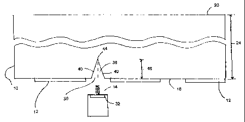
[0046] Fig. 4 shows one exemplary passive electronic component substrate,
a ceramic substrate 10, onto which a laser beam 14 is aimed. Ceramic
substrate 10 includes a first surface 18 and a second surface 20 that define
between them a substrate thickness 24. Ceramic substrate 10 also includes a
street 28 (shown in Fig. 6) and multiple electronic components 12, e.g.
resistors, that have been affixed on one of first substrate surface 18 or
second
substrate surface 20. The scribing method of the present invention can be
performed on either side of ceramic substrate 10 or both sides of ceramic
substrate 10. Single-sided substrate scribing (shown in Fig. 5A) is preferred
when scribing chip resistor substrates, and double-sided substrate scribing
(shown in Fig. 5B) is preferred when scribing chip capacitor substrates.
(0047] A laser scribe machine including a laser 32 is aligned with street 28
using a beam positioning system as described above. The portion of ceramic
substrate 10 coextensive with street 28 is then ablated to form a trench 36.
Trench 36 may be formed by a single pass or multiple passes of laser beam 14,
CA 02532033 2006-O1-10
WO 2005/008849 PCT/US2004/022227
12
depending on the operational parameters of the laser system, the thickness,
density, and type of ceramic substrate being scribed, and any manufacturing
constraints. The length of trench 36 typically runs the entire usable length
or
width of the ceramic substrate surface. Trench 36 includes a trench length
that
is preferably coextensive with street 28 and a trench width that is preferably
less than about 30,~m and more preferably between about 20,~m and about
30 Nm, as established by the laser beam spot size.
[0048] Multiple trenches may be created along streets 28 to form a grid on
the ceramic substrate surface as shown in Fig. 6. The multiple trenches may
be formed in any of the ways commonly known to those skilled in the art,
including scribing one scribe line with multiple passes before scribing
additional
scribe lines, scribing each scribe line in the grid with a first pass before
scribing
each line with additional passes, and scribing using an alternate pattern
approach. (An example of alternate pattern scribing would be, for a set of
multiple streets arranged side-by-side lengthwise, forming scribe lines in
alternating sequence along streets from two nonoverlapping subsets of the
streets in the set.) Because ceramic substrates retain heat, the preferred
method of scribing grids having a tight pitch (grids in which adjacent scribe
lines
are positioned less than 400 microns apart) involves scribing, in an alternate
pattern, each individual scribe line with a first pass before scribing each
line
with additional passes. The time elapsed between the first and second passes
for each scribe line facilitates heat dissipation and thereby minimizes the
incidence of heat build-up-based chipping and cracking of the ceramic
substrate.
[0049] Trench 36 further includes two inclined side walls 40 extending from
the ceramic substrate surface 18 and converging to form a clearly defined snap
line 44 at the bottom of trench 36 such that it has a cross section that is
approximately triangular in shape (a wide opening and an apex 44). In Fig. 4,
trench 36 has a trench depth 48 extending from either first surface 18 (Fig.
4) or
second surface 20 of ceramic substrate 10 to the bottom of trench 36 where the
two side walls 40 converge to form snap line 44 having a high stress
concentration. Trench depth 48 is preferably sufficiently shallow such that
CA 02532033 2006-O1-10
WO 2005/008849 PCT/US2004/022227
13
trench 36 does not appreciably penetrate ceramic substrate thickness 24,
thereby minimizing the formation of microcracks extending perpendicular to the
scribe line. Trench depth 48 is dependent on the circuit size and substrate
thickness and is preferably between about 5% and 40% of substrate thickness
24. Trench depth 48 can be controlled by selecting the appropriate power
setting and duration of application for laser beam 14. Optimal scribe line
depth
is dependent on the substrate materials) into which the scribe line is formed.
Thus the optimal value will be established by the properties of each substrate
material and each set of laser operating parameters.
[0050] Ceramic substrate 10 is then broken into multiple pieces by
application of a tensile breakage force perpendicular to the scribe line.
Trench 36 preferably has a triangular cross-sectional shape such that the
application of a breakage force on both sides of trench 36 causes ceramic
substrate 10 to cleanly break along snap line 44. The resulting multiple
circuit
components include side margins that were originally trench side walls 40.
[0051] A plurality of trenches 36 may be formed on ceramic substrate 10
using the method of the present invention. One exemplary method by which a
plurality of circuit components can be made is shown in Fig. 6, showing a
scribe
grid 56 on a surface of ceramic substrate 10. Scribe grid 56 includes
horizontal
(x-axis) 28h and vertical (y-axis) 28v streets that define an array of
separate
regions, each corresponding to an individual circuit component. Scribe grid 56
also includes trenches 36 that are coextensive with horizontal (x-axis) 28h
and
vertical (y-axis) 28v streets.
[0052] Instead of, or in addition to, covering with a sacrificial layer the
ceramic substrate surface that will be impinged by laser beam 14, as is well
known to persons skilled in the art, laser cutting may be performed from the
backside 20 of the ceramic surface so that laser-generated debris becomes
irrelevant. Backside alignment can be accomplished with laser or other
markings or alignment through-holes made from front side 18 of ceramic
substrate 10. An exemplary alignment hole is shown in Fig. 11. Alternatively,
backside alignment can be accomplished using edge alignment and/or
calibration with a camera view, as are known to persons skilled in the art.
CA 02532033 2006-O1-10
WO 2005/008849 PCT/US2004/022227
14
[0053] The following examples demonstrate exemplary lasers and
operational parameters that cooperate to effect the depthwise removal of fired
and green (unfired) ceramic substrate materials to form the clearly defined,
snap line of the present invention.
EXAMPLE 1. Lower Power, Higher Repetition Rate Micromachinina
[0054] A scribe line was formed on a fired ceramic substrate material having
a thickness of 0.913 mm using a Model No. V03 laser, manufactured by
LightWave Electronics of Mountain View, CA, emitting a 25 micron Gaussian
beam and positioned in a Model No. 5200 laser system, manufactured by
Electro Scientific Industries. The process was run at an effective rate of 0.5
mmls (actual rate = 25mmls l repetitions). The operational parameters used
are listed in Table I.
Table I. Operational Parameters.
PRF 3 kHz
Avg. Power 1.4 W
Min. Power 1.4 W
Max. Power 1.4 W
Wavelength 355 nm
Stability* 100%
Energy/Pulse 466.7 uJ
Fluence 95 Jicm2
Speed 25 mmls
Bite Size 8.33 microns
Spot Diameter 25 microns
No. of 1 to 50
Repetitions
* stability
is a measure
of pulse-to-pulse
laser stability.
$ Repetitions
are the number
of passes the
laser beam makes
over a specific
area.
(0055] Following formation of the scribe line, the ceramic material was
broken along the line to form two singulated circuit components that were
CA 02532033 2006-O1-10
WO 2005/008849 PCT/US2004/022227
examined with a light microscope to evaluate cut quality, depth, and features.
The circuit component side edges were clean and had no debris. The walls of
the cut were slightly tapered due to the Gaussian beam profile. Overall, the
process produced a clean cut having good edges and a clean break. Data
relating to the depth of the cut vs. the number of repetitions and the
percentage
of cut (cut/total thickness of the fired ceramic material) are shown in Table
Il,
which suggests that multiple repetitions are preferred when using these
operational parameters.
Table II. Tesf Results for Depth of Cut, Percent Gut, and Depth per Pass
Pass Depth of Cut Percent Depth per Pass
(mm) Cut (mm)
4 0.014 1.53% 0.014
5 0.017 1.86% 0.003
6 0.023 2.52% 0.006
7 0.029 3.18% 0.006
8 0.029 3.18% 0
9 0.031 3.40% 0.002
10 0.032 3.50% 0.001
11 0.038 4.16% 0.006
12 0.038 4.16% 0
13 0.046 5.04l0 0.008
0.08 8.76% 0.034
50 0.165 18.07% 0.085
EXAMPLE 2. Higher Power, Lower Repetition Rate Micromachinine~
[0056 A scribe line was formed on a fired ceramic substrate material having
a thickness of 0.962 mm using a Model No. Q301 laser, manufactured by
LightWave Electronics of Mountain View, CA, emitting a 25 micron Gaussian
beam and positioned in a Model No. 5200 laser system, manufactured by
Electro Scientific Industries. The operational parameters used are listed in
Table III.
CA 02532033 2006-O1-10
WO 2005/008849 PCT/US2004/022227
16
Table III. Operational Parameters
PRF 15 kHz
Avg. Power 7.27 W
Min. Power 7.25 W
Max. Power 7.29 W
Wavelength 355nm
Stability* 99.3%
EnergylPulse 484.7 uJ
Fluence 98.7 Jlcm2
* Stability
is a measure
of pulse-to-pulse
laser stability.
[0057] Three separate trials were performed at varying speeds and bite
sizes as indicated in Tables IV, V, and VI.
Table IV. Trial #7
Speed 25 mm/s
Bite Size 1.667 microns
Spot Diameter 25 microns
No. of Repetitions1 to 2
Effective Speed12.5 mm/s
Table V. Trial #2
Speed 50 mm/s
Bite Size 3.33 microns
Spot Diameter 25 microns
No. of Repetitions2
Effective Speed25 mm/s
CA 02532033 2006-O1-10
WO 2005/008849 PCT/US2004/022227
17
Table VI. Trial #3
Speed 100 mm/s
Bite Size 6.66 microns
Spot Diameter 25 microns
No. of Repetitions3
Effective Speed33 mm/s
[0058] Following formation of each scribe line, the ceramic material was
broken along the line to form two singulated circuit components that were
examined with a light microscope to evaluate cut quality, depth, and features.
The edge break areas on the scribed circuit components formed by lasers
scribing at speeds of 50mm/s and 100mm/s produced very clean edges along
the snap line. An edge taper of approximately 20 microns was seen on the
edges, which may be attributed to a scribe line width of approximately
45 microns.
[0059] Data regarding the depth of cut vs. the number of repetitions (passes)
for each of the three trials described in Tables IV to VI are shown in Table
VII.
CA 02532033 2006-O1-10
WO 2005/008849 PCT/US2004/022227
18
Table VII. Depth of Cut per Repetition for Lasers Operating at Speeds of
25 mm/s, 50 mmls, and 700 mmls.
25 mm/s
Pass Depth of Cut Percent Cut Depth per Pass
(mm) (mm)
1 0.019 1.98% 0.019
2 0.027 2.81 % 0.008
3 0.038 3.95% 0.011
50 mm/s
Pass Depth of Cut Percent Cut Depth per Pass
(mm) (mm)
1 0.014 1.46% 0.014
2 0.017 1.77% 0.003
3 0.023 2.39% 0.006
100 mmis
Pass Depth of Cut Percent Cut Depth per Pass
(mm)~ (mm)
1 0.01 1.04% 0.01
2 0.021 2.18% 0.011
[0060] A comparison of Tables II and VII shows that the increased power
used in Example 2 results in an increased ceramic material removal rate.
Consequently, a higher power per pulse laser system operating at a higher
repetition rate is preferred.
EXAMPLE 3. HicLher Power, Lower Repetition Rate Micromachinina
(0061] A scribe line was formed on a fired ceramic substrate material having
a thickness of approximately 100 microns using a Model No. Q302 laser,
manufactured by LightWave Electronics of Mountain View, CA, emitting a 25
micron Gaussian beam and positioned in a Model No. 5200 laser system,
manufactured by Electro Scientific Industries. The operational parameters used
are listed in Table VIII.
CA 02532033 2006-O1-10
WO 2005/008849 PCT/US2004/022227
19
Table VIII. Operational Parameters
Effective
Wave- Avg. RepetitionEnergy/No. Pulse Max. Spot ,
of
lengthPower Rate Pulse Repe-Width Power Diameter Fluence
(nm) (W) (kHz) (,uJ) titions(ns) (kw) (,um) (J/cm~)
355 3.9 50 78 1 25 3.12 30 1.10
[0062] The laser beam was moved at a programmed speed of 100 mm/s
and an effective speed of 50 mmls. The total depth of the scribe line was
approximately 28 microns. Because the bite size was approximately 2 microns,
there was significant overlap in each of the two repetitions. Following
formation
of the scribe line, the ceramic material was broken along the line to form two
singulated circuit components that were examined with a light microscope to
evaluate cut quality, depth, and features. The edge break areas on the scribed
circuit components lacked significant slag residue.
EXAMPLE 4. UV Laser Scribing of a Green Ceramic Substrate
[0063] A scribe line was formed in a green (unfired) MLCC substrate having
a thickness of 800 pm using a Model No. Q301 laser, manufactured by
LightWave Electronics, emitting a 25 micron Gaussian beam that was
positioned in a Model No. 4420 laser system, manufactured by Electro
Scientific Industries. The operational parameters used are listed in Table IX.
Table IX. Operational Parameters
Wave- Avg. RepetitionRepetitionNo. Bite Beam Cut Lens
of
length Power Rate Rate Repe- Size Speed Depth
(nm) (W) (kHz) (kHz) titions(um) (mmls) (um)
355 8.1 10 10 5-10 5 50 60 25
mm
[0064] Fig. 9 is a scanning electron micrograph showing a side view of a
scribe line that was formed in the green (unfired) MLCC substrate. As shown in
Fig. 9, the trench has clearly defined side walls that converge to form a
sharp
snap line. The cross-sectional shape of the trench is triangular.
CA 02532033 2006-O1-10
WO 2005/008849 PCT/US2004/022227
(0065] Following fiormation ofi the scribe line, the green MLCC substrate is
fired. Firing of the substrate plate results in shrinkage ofi the substrate.
Ceramic substrates typically undergo between about 10% and about 20%
shrinkage, dependent on numerous variables, such as particle size, particle
shape, distribution of dielectric and internal electrode metal powders, green
density of the substrate, method and operating parameters used to form the
plate (e.g., tape casting or screen printing), and dielectric formulation
composition. The applicants have found that the effective kerf depth of the
scribe line increases when the MLCC substrate is fired.
[0066] Following formation of the scribe line and firing of the substrate, the
MLCC material was broken along the scribe line to form multiple rows of
circuit
components (e.g., chip capacitors) that were examined with an optical
microscope to evaluate cut quality, depth, and features. Fig. 10 shows in the
plane of the figure the side margins of a row of chip capacitors. The chip
capacitor side edges were clean and had no debris. Overall, the process
produced a clean cut having good edges and a clean break. One advantage of
scribing green ceramic substrates is that deeper scribe lines can be formed in
green ceramic material because it is softer.
[0067] When forming chip capacitors, the ceramic substrate is preferably
scribed on both of the first and second substrate surfaces such that the
scribe
line on the first surface is spatially aligned with the scribe line on the
second
surface. This double-sided scribing is effected as follows: (1 ) alignment
holes
are drilled into the substrate, (2) a scribe line is formed on the first
surface using
the above-described method, (3) the substrate is flipped over and re-aligned
using the alignment holes, (4) a scribe line is formed on the second surface
using the above-described method such that the scribe line on the second
surface is spatially aligned with the scribe line on the first surface.
[0068] Multiple alignment holes are typically formed in the corners of the
substrate to facilitate alignment of the substrate when it is flipped over and
the
second surface is scribed. An exemplary alignment hole 80 is shown in Fig. 11.
Alignment hole 80 of Fig. 11 was formed on a green (unfired) MLCC substrate
having a thickness of 800 pm using a Model No. Q301 laser, manufactured by
CA 02532033 2006-O1-10
WO 2005/008849 PCT/US2004/022227
21
Lightwave Electronics, emitting a 25 micron Gaussian beam and positioned in a
Model No. 4420 laser system, manufactured by Electro Scientific Industries.
The operational parameters used are listed in Table X.
Table X. Operating Parameters.
Power Level Bite Size Beam Speed Repetition
(W) (um) (mm/s) Rate (kHz)
8.1 3 um 30 10
[0069] Alternative alignment methods, as described above, may be used in
connection with the formation of a scribe line on green material.
[0070] When the singulated circuit components form chip capacitors, edges
70 of trench 36 formed in substrate 10 are preferably edge rounded (as shown
in Figs 5B, 9, and 10). More specifically, side walls 40 meet first substrate
surface 18 to form edges 70 at first substrate surface 18 of substrate 10. It
is
the industry standard for these edges to be rounded. Edge rounding is
performed for two main reasons: (1 ) to round off the edges of the chips which
represent the primary source of mechanical stress concentration at the sharp
regions, thereby lowering the stress concentration in the edges and lessening
the chance of the termination coating chipping during processing and/or
handling and exposing the internal electrodes, and (2) facilitating uniform
end
termination chip coverage at the edges. Such rounding is effected by directing
the ultraviolet laser beam to remove substrate material at the edges to impart
curved shapes to them. Exemplary specifications for edge rounding are: an
apex-to-side ratio of <3 um and corner coverage of <20 um.
[0071] Examples 1-4 show that the formation of a region of high stress
concentration facilitates higher precision fracture of the ceramic substrate
such
that the interior integrity of each resulting ceramic substrate piece remains
substantially unchanged during and after application of the breakage force.
The ceramic substrate interior remains intact because the multiple depthwise
cracks that form in the ceramic substrate as a result of the application of
the
CA 02532033 2006-O1-10
WO 2005/008849 PCT/US2004/022227
22
breakage force propagate depthwise through the thickness of the ceramic
substrate in the region of high stress concentration rather than lengthwise
throughout the interior structure of each piece of ceramic substrate. This
facilitates cleaner fracture of the ceramic substrate into multiple circuit
components.
[0072] Also, the operating parameters of the laser beam minimize the
incidence of resolidification of the ceramic substrate material, decreasing
the
degree to which the side walls of the trench melt during application of the
laser
beam and thereby minimizing the formation of slag residue. Specifically, the
laser scribe method of the present invention causes absorption of most of the
laser energy by the portion of the ceramic substrate thickness removed by the
laser pulse. Such energy absorption ensures that virtually no heat is left
behind
to cause melting of the sidewalls of the trench. The lack of significant
resolidification and consequent clearly defined trench side walls results in
higher precision fracture of the ceramic substrate along the scribe line
because
the ablative (non-thermal) nature of the laser beam weakens the ceramic
substrate without disturbing the interior structure of the ceramic substrate.
The
minimal resolidification also results in superior and consistent edge quality;
the
smoother edges eliminate points of weakness from which microcracks may
originate. Fig. 7 is a SEM showing at 65x magnification the smooth and even
side edges of a ceramic substrate piece that was scribed in accordance with
the method of the present invention.
[0073] One benefit of UV laser cutting is that it consumes significantly less
material (kerfs of less than 50,~m wide and preferably less than 30,~m wide)
than does mechanical cutting (slicing lanes of about 300,um and dicing paths
of
about 150,~m) so that more circuit components can be manufactured on a
single substrate.
[0074] The method of the present invention also facilitates scribing a
substrate having an irregular shape that required off-axis alignment of the
substrate and the laser beam. Specifically, the method of the present
invention
can be used to form off axis scribe lines positioned at azimuthal angles
relative
to the normal. When forming a scribe line on non-orthogonal or offset
patterns,
CA 02532033 2006-O1-10
WO 2005/008849 PCT/US2004/022227
23
inspection of the passive electronic component substrate at various points may
be required. One exemplary beam positioning system for use in scribing this
type of passive electronic component is the beam positioning system in a Model
4420 or 4370 UV-YAG Laser Scribing System manufactured by Electro
Scientific Industries, of Portland, Oregon, the assignee of the present
application.
(0075] Further, multi-layer ceramic components, such as MLCCs including a
copper, silver, or nickel layer, can be scribed using the method of the
present
invention without destroying the integrity of the other layers. In one
embodiment, the green layers may be stacked and then the resulting ceramic
filter structure may be fired. As shown in Fig. 8, ceramic filter 48 may
include a
chip 50 that is coated with a laminate 52 and a copper, silver, or nickel
hermetic
coating 54. Chip 50 sits atop a ceramic substrate 62. Prior art methods of
mechanically sawing through copper hermetic coating 54 unacceptably
damaged laminate 52. Also, due to the ductile nature of copper, mechanically
sawing the top layer is unacceptably slow. The method of the present invention
allows copper hermetic layer 54 of ceramic filter 48 to be cut with a UV laser
beam having an energy and spot size sufficient to singulate copper hermetic
coating 54 and ceramic substrate 62 without damaging laminate 52. The UV
laser used in connection with the method of the present invention may be
programmed to cut through copper hermetic coating 54 and to leave in ceramic
substrate 62 a trench having a snap line along which ceramic substrate 62 may
be singulated into separate, nominally identical circuit components.
Alternatively, the UV laser used in connection with the method of the present
invention may be programmed to cut through copper hermetic coating 54
without affecting ceramic substrate 62. The laser may then be reprogrammed
to have an energy and spot size sufficient to form a scribe line in accordance
with the method of the present invention along which ceramic substrate 62 may
be singulated into separate, nominally identical circuit components.
(0076] In summary, the method of the present invention can be used to form
scribe lines in various types of passive electronic component substrates and
singulated to form various electronic components. A list of exemplary
electronic
CA 02532033 2006-O1-10
WO 2005/008849 PCT/US2004/022227
24
components includes chip resistors: chip capacitors; inductors; filters;
varistors
(including, but not limited to, metal oxide varistors, multilayer varistors,
and disc
varistors); thermistors; electronic components based on magnetic materials
such as ferrite beads and transformers; electronic components based on
piezoelectric ceramics such as transducers and sensors; electronic
components based on opto-electronic ceramics such as optical switches and
color filters; and LTCC and HTCC packages.
[0077] Lastly, ceramic substrates having metal-laden streets extending
along either, or both, of the x- and y-axis may similarly be singulated using
the
method of the present invention.
[0078] It will be obvious to those having skill in the art that many changes
may be made to the details of the above-described embodiment of this
invention without departing from the underlying principles thereof. The scope
of
the present invention should, therefore, be determined only by the following
claims.