Note: Descriptions are shown in the official language in which they were submitted.
CA 02533191 2006-01-20
WO 2005/008711 PCT/IL2004/000671
-1-
ELECTRON EMISSION DEVICE
FIELD OF THE INVENTION
This invention relates to an electron emission device, such as a diode or
triode structure.
BACKGROUND OF THE INVENTION
Diode and triode devices are widely used in the electronics. One class of
these devices utilize the principles of vacuum microelectronics, namely, their
operation is based on ballistic movement of electrons in vacuum [Brodie,
Keynote
address to the first international vacuum microelectronics conference, June
1988,
IEEE Trans. Electron Devices, 36, 11 pt. 2 2637, 2641 (1989); I. Brodie, C.A.
Spindt, in "Advances in Electronics and Electron Physics", vol. 83 (1992), p.
1-
106]. According to the principles of vacuum microelectronics, electrons are
ejected
from a cathode electrode by field emission and tunnel through the barrier
potential,
when a very high electric field (more than 1 V/nm) is locally applied [R.H.
Fowler,
L.W. Nordheim, Proc. Royal Soc. London Al19 (1928), p. 173].
U.S. Patent No. 5,834,790 discloses a vacuum microdevice having a field-
emission cold cathode. This device includes first electrode and second
electrodes.
The first electrode has a projection portion with a sharp tip. An insulating
film is
formed in the region of the first electrode, excluding the sharp tip of the
projection
portion. The second electrode is formed in a region on the insulating film,
excluding the sharp tip of the projection portion. A structural substrate is
bonded to
the lower surface of the first electrode and has a recess portion in the
bonding
surface with the lower surface of the first electrode. The recess portion has
a size
CA 02533191 2006-01-20
WO 2005/008711 PCT/IL2004/000671
-2-
large enough to cover a recess reflecting the sharp tip of the projection
portion
formed on the lower surface of the first electrode. The interior of the recess
portion
formed in the structural substrate communicates with the atmosphere outside
the
device. A support structure is formed on the surface of the second electrode
to
surround each projection portion formed on the first electrode. With this
structure, a
vacuum microdevice can be provided which can suppress variations in
characteristics due to voids and exhibit excellent long-term reliability.
Triodes (transistors) of another class are semiconductor devices based on the
principles of "solid state microelectronics", where the charge carriers are
confined
within solids and are impaired by interaction with the lattice [S.M. Sze,
Physics of
semiconductor devices, Interscience, 2nd edition, New York]. In the devices of
this
kind, a current is conducted within semiconductors, so the moving velocity of
electrons is affected by the crystal lattices or impurities therein. A
fundamental
drawback of active electronic devices based on semiconductors is that
electrons
transport is impeded by the semiconductor crystal lattice, which places a
limit on
both the miniaturization and the switching speed of such devices.
Vacuum microelectronic devices have potential advantages over solid-state
microelectronic devices. Vacuum microelectronic devices have a high degree of
immunity to hostile environment conditions (such as temperature and radiation)
since they are based only on metals and dielectrics. These devices can achieve
very
high operation frequencies, because the electrons' velocity is not limited by
interactions with the lattice [T. Utsumi, IEEE Tans. Electron Devices, 3
8,10,2276
(1991)]. In general, vacuum microelectronics devices have excellent output
circuit
(power delivery loop) characteristics: low output conductance, high voltage
and
high power handling capability. However, their input circuit (control loop)
characteristics are relatively poor: they have low current capabilities, low
transconductance, high modulation/turn-on voltage and poor noise
characteristics.
As a result, despite the tremendous research efforts in this field, these
devices found
only very few applications, especially as RF signal amplifiers and sources [S.
lannazzo, Solid State Electronics, 36, 3, 301 (1993)].
CA 02533191 2006-01-20
WO 2005/008711 PCT/IL2004/000671
-3-
Most of the current electronics is based on devices which are made from
Si or compound semiconductor based structures. Because of the intrinsic
resistivity of these devices, the electrons' transmission through the device
causes
the creation of heat. This heat is the main obstacle in the attempts to
maximize
the number of transistors within an integrated circuit per a given area.
Semiconductor devices utilizing microtip type vacuum transistors have
been developed. Here, electrons move in vacuum and thus, at the highest speed.
Therefore, the vacuum transistors can be operated at ultra speeds. However,
they
suffer from disadvantages in that they are unstable, have relatively short
lifetime,
and require relatively high voltages for their operation.
U.S. Patent No. 6,437,360 discloses a MOSFET-like flat or vertical
transistor structure presenting a Vacuum Field Transistor (VFT), in which
electrons travel a vacuum free space, thereby realizing the high speed
operation
of the device utilizing this structure. The flat type structure is formed by a
source
and a drain, made of conductors, which stand at a predetermined distance apart
on a thin channel insulator with a vacuum channel therebetween; a gate, made
of
a conductor, which is formed with a width below the source and the drain, the
channel insulator functioning to insulate the gate from the source and the
drain;
and an insulating body, which serves as a base for propping up the channel
insulator and the gate. The vacuum field transistor comprises a low work
function material at the contact regions between the source and the vacuum
channel and between the drain and the vacuum channel. The vertical type
structure comprises a conductive, continuous circumferential source with a
void
center, formed on a channel insulator; a conductive gate formed below the
channel insulator, extending across the source; an insulating body for serving
as a
base to support the gate and the channel insulator; an insulating walls which
stand over the source, forming a closed vacuum channel; and a drain formed
over
the vacuum channel. In both types, proper bias voltages are applied among the
gate, the source and the drain to enable electrons to be field emitted from
the
source through the vacuum channel to the drain.
CA 02533191 2006-01-21
21-11-2005 EPO -DG J IL0400671
21, 11. 2005
3a- '03
GB 347544 describes a gas or vapour filled photo-electric cell. The cell
has a grid at a distance from a cathode equal to or less than the free path of
an
electron in the filling. An anode consists of a ring through which light
passes.
The grid is raised to a potential not greater than 10 volts, and preferably 1-
5
volts, so as to prevent electrons returning to the cathode. The filling may be
argon or neon at a pressure of 1 mm of mercury.
US 4,721,885 discloses very high speed integrated microelectronic tubes.
An array of microelectronic tubes includes a plate-like substrate upon which
an
array of sharp needle-like cathode electrodes is located. Each tube in the
array
includes an anode electrode spaced from the cathode electrode. Each tube
contains gas at a pressure of between about 1/100 and 1 atmosphere, and the
spacing between the tip of the cathode electrodes and anode electrodes is
equal to
or less than about 0.5 m. The tubes are operated at voltages such that the
mean
free path of electrons traveling in the gas between the cathode and anode
electrodes is equal to or greater than the spacing between the tip of the
cathode
electrode and the associated anode electrode.
US 4,990,766 discloses a solid state electron amplifier. This microscopic
voltage controlled field emission electron amplifier device consists of a
dense
array of field emission cathodes with individual cathode impedances employed
to
modulate and control the field emission currents of the device.
These impedances are selected to be sensitive to an external stimulus such as
light, x-rays, infrared radiation or particle bombardment; so that the field
emission current varies -spatially in proportion to the intensity of the
controlling
stimulus. The device may function as a solid state image convertor or
intensifier,
when a phosphorus screen or other suitable responsive element is provided.
WO 96/10835 discloses a print head utilizing a field emission CRT for an
optical printer for printing on photosensitive surfaces. A plurality of small
electron sets consisting of cathode emitting cones in an anode aperture form a
gap which is less than the electron mean free path in ambient atmosphere and
the
sets are preferably closely spaced to form a substantially columnated beam.
AMENDED SHEET
CA 02533191 2006-01-21
21-11-2005 IL0400671
-3b-
A third electrode preferably accelerates and cleans up the beam which is
separated from the cathode. The beam is then incident upon a luminophor film
which is excited, thereby generating light. The light is transmitted through a
transmissive face plate such as a fiber optic face plate where it is incident
upon
the photosensitive material.
a
AMENDED SHEET
CA 02533191 2006-01-20
WO 2005/008711 PCT/IL2004/000671
-4-
SUMMARY OF THE INVENTION
There is a need in the art to significantly improve the performance of
electronic devices in general and transistors in particular and facilitate
their
manufacture and operation, by providing a novel electron emission device.
The electron emission device according to the present invention is based on
a new technology, which allows for eliminating the need for or at least
significantly
reducing the requirements to vacuum environment inside the device, allows for
effective device operation with a higher distance between Cathode and Anode
electrodes, as well as more stable and higher-current operation, as compared
to the
conventional devices of the kind specified, practically does not suffer from
large
energy dissipation, and is robust vis a vis radiation. This is achieved by
utilizes the
photoelectric effect, according to which photons are used for ejecting
electrons
from a solid conductive material, provided the photon energy exceeds the work-
function of this conductive material.
The device of the present invention is configured as an electron emission
switching device. The term "switching" signifies affecting a change in an
electric
current through the device (current between Cathode and Anode), including such
effects as shifting between operational and inoperational modes, modifying the
electric current, amplifying the current, etc. Such a switching may be
implemented
by varying the illumination of Cathode while keeping a certain potential
difference
between the electrodes of the device, or by varying a potential difference
between
the electrodes of the device while maintaining illumination of the Cathode, or
by a
combination of these techniques.
According to one broad aspect of the present invention, there is provided
an electron emission device comprising an electrodes' arrangement including at
least one Cathode electrode and at least one Anode electrode, the Cathode and
Anode electrodes being arranged in a spaced-apart relationship; the device
being
configured to expose said at least one Cathode electrode to exciting
illumination
to thereby cause electrons' emission from said Cathode electrode, the device
being operable as a photoemission switching device.
CA 02533191 2006-01-20
WO 2005/008711 PCT/IL2004/000671
-5-
A gap between the first and second electrodes may be a gas-medium gap
(e.g., air) or vacuum gap. A gas pressure in the gap is sufficiently low to
ensure
that a mean free path of electrons accelerating from the Cathode to the Anode
is
larger than a distance between the Cathode and the Anode electrodes (larger
than
the gap length).
The electrodes may be made from metal or semiconductor materials.
Preferably, the Cathode electrode has a relatively low work function or a
negative electron affinity (like in diamond and cesium coated GaAs surface).
This can be achieved by making the electrodes from appropriate materials
or/and
by providing an organic or inorganic coating on the Cathode electrode (a
coating
that creates a dipole layer on the surface which reduces the work function).
The Cathode electrode may be formed with a portion thereof having a
sharp edge, e.g., of a cross-sectional dimension substantially not exceeding
60nm (e.g., a 30nm radius).
The device is associated with a control unit, which operates to effect the
switching function. The control unit may operate to maintain illumination of
the
Cathode electrode and to affect the switching by affecting a potential
difference
between the Cathode and Anode and thereby affect an electric current between
them. Alternatively, the control unit may effect the switching function by
appropriately operating the illuminating assembly to cause a change in the
illumination, and thus affect the electric current.
The electrodes' arrangement may include an array (at least two)-Cathode
electrodes associated with one or more Anode electrodes; or an array (at least
two) Anode electrodes associated with the same Cathode electrode. Considering
for example, multiple Anode and single Cathode arrangement, the control unit
may operate to maintain illumination of the Cathode electrode and to control
an
electric current between the Cathode electrode and each of the Anode
electrodes
by varying a potential difference between them. Generally speaking, various
combinations of Cathode and Anode electrodes may be used in the device of the
present invention, for example the electrodes' arrangement may be in form of a
CA 02533191 2006-01-20
WO 2005/008711 PCT/IL2004/000671
-6-
pixilated structure. The Cathode and Anode electrodes may be accommodated in
a common plane or in different planes, respectively.
The electrodes' arrangement may include at least one additional electrode
(Gate) electrically insulated from the Cathode and Anode electrodes. The Gate
electrode may and may not be planar (e.g., cylindrically shaped). The Gate
electrode may be configured as a grid located between the Cathode and Anode
electrodes. The Gate electrode may be accommodated in a plane spaced-apart
and parallel to a plane where the Cathode and Anode electrodes are located; or
the Cathode, Anode and gate electrodes are all located in different planes.
The Gate electrode may be used to control an electric current between the
Cathode and Anode electrodes. For example, the control unit operates to
maintain certain illumination of the Cathode, and affect the electric current
between the Cathode and Anode (kept at a certain potential difference between
them) by varying a voltage supply to the Gate.
The electrodes' arrangement may include an array of Gate electrodes
arranged in a spaced-apart relationship and electrically insulated from the
Cathode and Anode electrodes. The device may for example be operable to
implement various logical circuits, or to sequentially switch various electric
circuits.
Generally, the electrodes arrangement may be of any suitable
configuration, like tetrode, pentode, etc., for example designed for lowering
capacitance.
The electrodes' arrangement may include an array of Anode electrodes
associated with a pair of Cathode and Gate electrodes. For example, the
control
unit operates to maintain certain illumination of the Cathode electrode, and
control an electric current between the Cathode and the Anode electrodes by
varying a voltage supply to the Gate electrode.
The illuminating assembly may include one or more light sources, and/or
utilize ambient light. In some non limiting examples, the illuminating
assembly
may include a low pressure discharge lamp (e.g., Hg lamp), and/or a high
CA 02533191 2006-01-20
WO 2005/008711 PCT/IL2004/000671
-7-
pressure discharge lamp (e.g., a Xe lamp), and/or a continuous wave laser
device,
and/or a pulsed laser device (e.g., high frequency), and/or at least one non-
linear
crystal, and/or at least one light emitting diode.
The Cathode and Anode electrode may be made from ferromagnetic
materials, different in that their magnetic moment directions are opposite,
thus
enabling implementation of a spin valve (Phys Rev. B, Vol. 50, pp. 13054,
1994). The device may thus be shiftable between its inoperative and operative
positions by shifting one of the Cathode and Anode electrodes between its SPIN
UP and SPIN DOWN states. To this end, the device includes a magnetic field
source operable to apply an external magnetic field to the electrodes'
arrangement. The application of the external magnetic field shifts one of the
electrodes between its SPIN UP and SPIN DOWN states.
The Cathode electrode may be made from non-ferromagnetic metal or
semiconductor and the Anode electrode from a ferromagnetic material. In this
case, the illuminating assembly is configured and operable to generate
circular
polarized light to cause emission of spin polarized electrons from the
Cathode.
The device is shiftable between its operative and inoperative positions by
varying
the polarization of light illuminating the Cathode, or by shifting the Anode
electrode between SPIN UP and SPIN DOWN high-transmission states. The
change in polarization of illuminating light may be achieved by using one or
more light sources emitting light of specific polarization and a polarization
rotator (e.g., 2J4 plate) in the optical path of emitted light; or by using
light
sources emitting light of different polarization, respectively, and
selectively
operating one of the light sources.
The Cathode electrode may be located on a substrate transparent for a
wavelength range used to excite the Cathode electrode. In this case, the
illuminating assembly may be oriented to illuminate the Cathode electrode
through the transparent substrate. Alternatively or additionally, a substrate
carrying the Anode electrode (and possibly also the Anode electrode) may be
transparent and located in a plane spaced from that of the Cathode, thereby
CA 02533191 2006-01-20
WO 2005/008711 PCT/IL2004/000671
-8-
enabling illumination of the Cathode through the Anode-carrying substrate
regions outside the Anode (or through the Anode-carrying substrate and the
Anode, as the case may be).
Based on the recent developments in nano-technology, in general, and in
optical lithography in particular, the device of the present invention can be
manufactured as a low-cost sub-micron structure. The electrodes' arrangement
is
an integrated structure including first and second substrate layers for
carrying the
Cathode and Anode electrodes; and a spacer layer structure between the first
and
second substrate layers. The spacer layer structure is patterned to define a
gap
between the Cathode and Anode electrodes. The spacer layer structure may
include at least one dielectric material layer. For example, the spacer layer
structure includes first and second dielectric layers and an electrically
conductive
layer (Gate) between them. Either one of the first and second substrates or
both
of them are made of a material transparent with respect to the exciting
wavelength range thereby enabling illumination of the Cathode.
The electrodes' arrangement may be an integrated structure configured to
define an array of sub-units, each sub-unit being constructed as described
above.
Namely, the integrated structure includes a first substrate layer for carrying
an
array of the spaced-apart Cathode electrodes; a second substrate layer for
carrying an array of the spaced-apart Anode electrodes; and a spacer layer
structure between the first and second substrate layers. The spacer layer
structure
is patterned to define an array of spaced-apart gaps between the first and
second
arrays of electrodes.
According to another aspect of the invention, there is provided, an
electron emission device comprising an electrodes' arrangement including at
least one Cathode electrode and at least one Anode electrode arranged in a
spaced-apart relationship; the device being configured to expose said at least
one
Cathode electrode to exciting illumination to cause electron emission
therefrom,
the device being operable as a photoemission switching device by affecting an
electric current between the Cathode and Anode electrodes, the switching being
CA 02533191 2006-01-20
WO 2005/008711 PCT/IL2004/000671
-9-
effectible by at least one of the following: varying the illumination of the
:the
Cathode electrode, and varying an electric field between the Cathode and Anode
electrodes.
The electric field may be varied by varying a potential difference between
the Cathode and Anode electrodes, or when using at least one Gate electrode by
varying a voltage supply to the Gate electrode.
According to yet another aspect of the invention, there is provided, an
electron emission device comprising an electrodes' arrangement including at
least one Cathode electrode, at least one Anode electrode, and at least one
additional electrode arranged in a spaced-apart relationship; the device being
configured to expose said at least one Cathode electrode to exciting
illumination
to thereby cause electrons' emission from said at least one illuminated
Cathode
electrode towards said at least one Anode electrode; the device being operable
as
a photoemission switching device by affecting an electric current between the
Cathode and Anode electrodes, the switching being effectible by at least one
of
the following: varying the illumination of the Cathode electrode, and varying
an
electric field between the Cathode and Anode electrodes.
According to yet another aspect of the invention, there is provided, an
electron emission device comprising an electrodes' arrangement including at
least one Cathode electrode and at least one Anode electrode, the Cathode and
Anode electrodes being arranged in a spaced-apart relationship with a gas-
medium gap between them; the device being configured to expose said at least
one Cathode electrode to exciting illumination to thereby cause electrons'
emission from said at least one illuminated Cathode electrode, the device
being
operable as a photoemission switching device.
According to yet another aspect of the invention, there is provided an
electron emission device comprising an electrodes' arrangement including at
least one Cathode electrode, at least one Anode electrode, and at least one
additional electrode arranged in a spaced-apart relationship; the device being
configured to expose said at least one Cathode electrode to exciting
illumination
CA 02533191 2006-01-20
WO 2005/008711 PCT/IL2004/000671
-10-
to thereby cause electrons' emission from said at least one illuminated
Cathode
electrode towards said at least one Anode electrode; the device being operable
as
a photoemission switching device
According to yet another aspect of the invention, there is provided an
integrated device comprising at least one structure operable as an electrons'
emission unit, said at least one structure comprising at least one Cathode
electrode and at least one Anode electrode that are carried by first and
second
substrate layers, respectively, which are spaced from each other by a spacer
layer
structure including at least one dielectric layer, the spacer layer structure
being
patterned to define a gap between the Cathode and Anode electrodes, at least
one
of the first and second substrates being made of a material transparent with
respect to certain exciting radiation to thereby enable illumination of the at
least
one Cathode electrode to cause electrons emission therefrom, the device being
operable as a photoemission switching device.
According to yet another aspect of the invention, there is provided an
integrated device comprising at least one structure operable as an electrons'
emission unit, said at least one structure comprising at least one Cathode
electrode and at least one Anode electrode that are carried by first and
second
substrate layers, respectively, which are spaced from each other by a spacer
layer
structure including first and second dielectric layers and an electrically
conductive layer between the dielectric layers, the spacer layer structure
being
patterned to define a gap between the Cathode and Anode electrodes, at least
one
of the first and second substrates being made of a material transparent with
respect to certain exciting radiation to thereby enable illumination of the
Cathode
electrode to cause electrons emission therefrom, the device being operable as
a
photoemission switching device.
According to yet another aspect of the invention, there is provided an
integrated device comprising an array of structures operable as electrons'
emission units, the device comprising a first substrate layer carrying the
array of
the spaced-apart Cathode electrodes, a second substrate layer carrying the
array
CA 02533191 2006-01-20
WO 2005/008711 PCT/IL2004/000671
-11-
of the spaced-apart Anode electrode; and a spacer layer structure between said
first and second substrates, the spacer layer structure including at least one
dielectric layer and being patterned to define an array of gaps, each between
the
respective Cathode and Anode electrodes, at least one of the first and second
substrates being made of a material transparent with respect to certain
exciting
radiation to thereby enable illumination of the Cathode electrode to cause
electrons emission therefrom, the device being operable as a photoemission
switching device.
According to yet another aspect of the invention, there is provided, a
method of operating an electron emission device as a photoemission switching
device, the method comprising illuminating a Cathode electrode by certain
exciting radiation to cause electrons' emission from the Cathode electrode
towards an Anode electrode, and affecting the switching by at least one of the
following: controllably varying the illumination of the Cathode, and
controllably
varying an electric field between the Cathode and Anode electrodes.
As indicated above, Cathode and Anode electrodes may be spaced from
each other by a gas-medium gap (e.g., air, inert gas). Such a device may and
may
not utilize the photoelectric effect. Thus device is based on a new
technology, the
so-called "gas-nano-technology". This technique is free of the drawbacks of
the
vacuum microelectronics, and, contrary to the existing semiconductor based
electronics, does not suffer from large energy dissipation, and is robust vis
a vis
radiation. Such a gas-nano device of the present invention provides for
electrons'
passage in air or another gas environment. The device may be configured and
operable as a switching device, or a display device.
Thus, according to yet another aspect of the invention, there is provided
an electron emission device comprising an electrodes' arrangement including at
least one unit having at least one Cathode electrode and at least one Anode
electrode that are arranged in a spaced-apart relationship, the Anode and
Cathode
electrodes being spaced from each other by a gas-medium gap substantially not
exceeding a mean free path of electrons in said gas medium.
CA 02533191 2006-01-20
WO 2005/008711 PCT/IL2004/000671
-12-
BRIEF DESCRIPTION OF THE DRAWINGS
In order to understand the invention and to see how it may be carried out
in practice, preferred embodiments will now be described, by way of non-
limiting example only, with reference to the accompanying drawings, in which:
Fig. 1 is a schematic illustration of an electron photoemission switching
device according to one embodiment of the invention, operable as a diode
structure;
Fig. 2 is a schematic illustration of an electron photoemission switching
device according to another embodiment of the invention designed as a triode
structure;
Figs. 3A-3C show several examples of the electrodes' arrangement design
suitable to be used in the device of Fig. 2;
Fig. 4 exemplifies yet another configuration of an electron photoemission
switching device of the present invention, where the electrodes' arrangement
includes an array of Anode electrodes associated with a common Cathode
electrode;
Fig. 5 schematically illustrates yet another configuration an electron
photoemission switching device of the present invention;
Fig. 6 illustrates the experimental results of the operation of an electron
emission device of the present invention configured as the device of Fig. 1;
Figs. 7A to 7C show another experimental results illustrating the features of
the present invention, wherein Fig. 7A shows an electron photoemission
switching
device of the present invention designed as a simple planar triode structure;
and
Figs. 7B and 7C show the measurement results: Fig. 7B shows the volt-ampere
characteristics measured on the Anode for different voltages on the Gate-grid,
and
Fig. 7C shows the Anode current as a function of the Gate voltage for
different
voltages on the Anode;
Figs. 8A to 8E exemplify the implementation of an electron photoemission
switching device of the present invention in a micron scale, wherein Fig. 8A
shows
a device presenting a basic unit of a multiple-units device of Fig. 8B; and
Figs. 8C-
8E show electrostatic simulation of the operation of the device of Fig. 8A;
and
CA 02533191 2006-01-20
WO 2005/008711 PCT/IL2004/000671
- 13-
Figs. 9A to 9C illustrate yet another examples of an electron photoemission
switching device of the present invention configured and operable utilizing a
spintronic effect in a transistor structure.
DETAILED DESCRIPTION OF THE INVENTION
Referring to Fig. 1, there is schematically illustrated an electronic device
10
constructed according to one embodiment of the invention. The device is
configured and operable as an electron photoemission switching device. In the
present example, the device has a diode structure configuration. The device 10
comprises an electrodes' arrangement 12 formed by a first Cathode electrode
12A
and a second Anode electrode 12B that are arranged on top of a substrate 14 in
a
spaced-apart relationship with a gap 15 between them. The device is configured
to
expose the Cathode 12A to exciting radiation to cause electrons emission
therefrom
towards the Anode. As shown in the present example, the device includes an
illuminator assembly 20 oriented and operable to illuminate at least the
Cathode
electrode 12A to thereby cause emission of electrons from the Cathode towards
the
Anode.
The switching (i.e., affecting of an electric current between the Cathode and
Anode) is controlled by the illumination of the Cathode electrode and
appropriate
application of an electric field between the Anode and Cathode electrodes. For
example, the Cathode and Anode may be kept at a certain potential difference
between them, and switching is achieved by modifying the illumination
intensity.
Another example to effect the switching is by varying the potential difference
between the electrodes, while maintaining certain illumination intensity. Yet
another
example is to modify both the illumination and the potential difference
between the
electrodes. It should be noted that modifying the illumination may be achieved
in
various ways, for example by modifying the operational mode of a light
emitting
assembly, by modifying polarization or phase of emitted light, etc. The device
10 is
associated with a control unit 22 including inter alia a power supply unit 22A
for
CA 02533191 2006-01-20
WO 2005/008711 PCT/IL2004/000671
-14-
supplying voltages to the Cathode and Anode electrodes, and an appropriate
illumination control utility 22B for operating the illuminator 20.
The Cathode and Anode electrodes 12A and 12B may be made of metal or
semiconductor materials. The Cathode electrode 12A is preferably a reduced
work
function electrode. Negative electron affinity (NEA) materials can be used
(e.g.,
diamond), thus reducing the photon energy (exciting energy) necessary to
induce
photoemission. Another way to reduce the work function is by coating or doping
the Cathode electrode 12A with an organic or inorganic material (a coating 16
being exemplified in the figure in dashed lines) that reduces the work
function. For
example, this may be metal, multi-alkaline, bi-alkaline, or any NEA material,
or
GaAs electrode with cesium coating or doping thereby obtaining a work function
of
about 1-2eV. The organic or inorganic coating also serves to protect the
Cathode
electrode from contamination.
The illuminator assembly 20 can include one or more light sources operable
with a wavelength range including that of the exciting illumination for the
Cathode
electrode used in the device. This may be, but not limited to, a low pressure
lamp
(e.g., Hg lamp), other lamps (e.g. high pressure Xe lamp), a continuous wave
(CW)
laser or pulse laser (high frequency pulse), one or more non-linear crystals,
or one
or more light emitting diodes (LEDs), or any other light source or a
combination of
light sources.
Light produced by the illuminator assembly 20 can be directly applied to the
electrode(s) or through the transparent substrates 14 (as shown in the figure
in
dashed lines).
The Cathode and Anode electrodes 12A and 12B may be spaced from each
other by the vacuum or gas-medium (e.g., air, inert gas) gap 15. As shown in
the
figure by dashed lines, the entire device 10, or only electrodes' arrangement
thereof,
can be encapsulated and filled with gas. It should be understood that the gas
pressure is low enough to ensure that a mean free path of electrons
accelerating
from the Cathode to the Anode is larger than a distance (the length of the gap
15)
between the Cathode and the Anode electrodes, thereby eliminating the need for
CA 02533191 2006-01-20
WO 2005/008711 PCT/IL2004/000671
- 15-
vacuum between the electrodes or at least significantly reducing the vacuum
requirements. For example, for a 10 micron gap between the Cathode and Anode
layers, a gas pressure of a few mBar may be used. In other words, the length
of the
gap 15 between the electrodes 12A and 12B substantially does not exceed a mean
free path of electrons in the gas environment
It should however be understood that the principles of the present invention
(the Cathode illumination) can advantageously be used in the conventional
vacuum-based field emission device to thereby significantly reduce the
requirements to a low work function of the Cathode electrode material, and/or
geometry, and/or to reduce the need for a high electric field.
As shown in Fig. 1 in dashed lines, the Cathode electrode 12A may be
designed to have a very sharp edge 17, e.g., substantially not exceeding 60nm
in a
cross-sectional dimension (e.g., with a radius less than about 30nm). Such a
design
of the Cathode is typically used to enable the device operation at lower
electric
potential as compared to that with the flat-edge Cathode. It is, however,
important
to note that the use of illumination of the Cathode practically eliminates the
need
for making the Cathode with a sharp edge. Comparing the device of the present
invention (where illumination of the Cathode is used) to the convention
devices of
the kind specified, the device of the present invention is characterized by
better
current stability and less sensitivity to the changes in the electrodes'
surface effects,
as well as the possibility of achieving effective device operation at a larger
distance
between the Cathode and Anode, lower applied field, and no need for a sharp
edge
of the Cathode. The use of Cathode illumination provides for operating with
lower
voltages, i.e., energy of electrons reaching the Anode is lower, thus
preventing such
undesirable effects for Anode electrode as sputtering and evaporation.
Fig. 2 schematically illustrates an electron photoeinission switching device
100 of the present invention designed as a triode structure. To facilitate
understanding, the same reference numbers are used for identifying components
which are common in all the examples of the invention. The device 100 includes
an
electrodes' arrangement 12 formed by Cathode and Anode electrodes 12A and 12B
CA 02533191 2006-01-20
WO 2005/008711 PCT/IL2004/000671
-16-
spaced from each other by a gap 15 (vacuum or gas-medium gap), and a Gate
electrode 12C electrically insulated from the Cathode and Anode electrodes. In
the
present example, the Gate electrode 12C is located above the Anode 12B being
spaced therefrom by an insulator 18. An electrons' extractor (illuminator) 20
is
provided being accommodated so as to illuminate at least the Cathode
electrode,
either directly (as shown in the figure) or via an optically transparent
substrate 14.
In the configuration of Fig. 2, the electrodes 12B and 12C serve as,
respectively, Anode and switching control element. More specifically, a change
in
an electric current between the Cathode and Anode is affected by a selective
voltage
supply to the Gate, while certain illumination of Cathode and a certain
potential
difference between the Cathode and Anode are maintained.
It should, however, be understood that switching can be realized using
another configurations as well. For example by switching electrodes 12B and
12C,
by making electrodes 12B and 12C side by side, by omitting the "Gate"
electrode
12C at all and controlling the electric current between electrodes 12A and 12B
by
the voltage supply between them (as shown in the configuration of Fig. 1),
and/or
by varying the illumination intensity.
Figs. 3A-3C show in a self-explanatory manner several possible but not
limiting examples of the electrodes' arrangement design suitable to be used in
the
device 100.
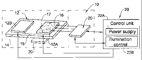
Fig. 4 exemplifies another configuration of an electron photoemission
switching device, generally designated 200, of the present invention. Here, an
electrodes' arrangement 12 includes a Cathode electrode 12A and an array
(generally at least two) spaced-apart Anode electrodes 12B - four such Anode
electrodes arranged in an arc-like or circular array being shown in the
present
example. The Anode electrodes 12B are appropriately spaced from the Cathode
electrode 12A depending on whether a vacuum or gas-medium gap between them
is used, as described above. An illuminator 20 is accommodated so as to
illuminate
the Cathode layer, which in the present example is implemented via an
optically
transparent substrate 14 carrying the Cathode electrode thereon. Each of the
CA 02533191 2006-01-20
WO 2005/008711 PCT/IL2004/000671
-17-
Cathode and Anode electrodes is separately addressed by the power supply.
During
the device operation, a control unit 22 operates the illuminator to maintain
certain
(or controllably vary) illumination of the Cathode electrode and thereby
enable
electrons extraction therefrom, and to selectively apply a potential
difference
between the Cathode and the respective Anode electrode. By this, a data stream
sequence can be created/multiplexed.
Reference is made to Fig. 5 schematically illustrating. yet another
configuration of a electron photoemission switching device 300 of the present
invention. The device 300 includes an electrodes' arrangement 12 and an
illuminator 20. The electrodes' arrangement 12 includes a Cathode electrode
12A,
and either a single Anode and multiple Gate electrodes or a single Gate and
multiple Anode electrodes. In the present example, a Gate electrode 12C and an
array of N Anode electrodes are used - five such Anode electrodes 12BWWW-
12B(5)
being shown in the figure. The illuminator 20 is accommodated to illuminate
the
Cathode electrode 12A. In the present example, the device is configured to
allow
Cathode illumination through the transparent substrate 14. A data stream
sequence
can be created/multiplexed by varying a voltage supply to the Gate 12C, while
maintaining a certain voltage supply to the Cathode and Anode electrodes and
maintaining certain illumination (or controllably varying the illumination) of
the
Cathode electrode 12A. The variation of the Gate 12C voltage determines the
electrons path from the Cathode to the Anode electrodes: increasing the
absolute
value of negative voltage on the Gate 12C results in sequential electrons
passage
from the Cathode to, respectively, Anode electrodes. 12W), 12B(2', 12W),
12B(4),
12B(5).
Fig. 6 illustrates the experimental results of the operation of an electrons'
emission device configured as the above-described device 10 of Fig. 1. A graph
G
presents the time variation of an electric current through the device while
shifting
the illuminating assembly (20 in Fig. 1) between its operative (Light On) and
inoperative (Light OFF) positions. In the present example, the Cathode and
Anode
CA 02533191 2006-01-20
WO 2005/008711 PCT/IL2004/000671
- 18-
electrodes are 45nm spaced from each other, and kept at 4.5V potential
difference
between them.
Reference is now made to Figs. 7A-7C, showing another experimental
results illustrating the features of the present invention.
Fig. 7A shows an electron photoemission switching device 400 of the
present invention designed as a simple planar triode structure. The device was
vacuum sealed, and a light source assembly (illuminator) 20 was used to
illuminate
a semi-transparent Photocathode 12A from outside via an optically transparent
substrate 14. Electrodes' arrangement 12 further includes an Anode electrode
12B,
and a Gate electrode 12C in the form of a grid between the Cathode and Anode.
The substrate 14 is a fused silica glass of a 500 m thickness. The
Photocathode 12A is made as a photo-emissive coating on the surface of the
substrate 14. The Photocathode is W -Ti (90%-10%) of a l5nm thickness
deposited
onto the substrate by E-Beam Evaporation (0.lnm/sec). The Gate-grid 12C is
formed by an array of spaced-apart parallel wires of metal with a 50 m
diameter
and a 150 m spacing between wires (center to center). The Anode electrode 12B
is
made from copper and has a thickness of 10mm. The light source 20 is a UV
source
(super pressure mercury lamp) with the light output power of 100mW in the
effective range (240-280nm). Light was guided onto the back side of the
Photocathode by a special Liquid Lightguide 21. The electrodes arrangement 12
was sealed in a ceramic envelope, and prior to measurements, air was pumped
out
of the envelope (using a simple vacuum pump) to obtain a 10"5 Torr pressure.
During the measurements, the Photocathode 12A was kept grounded.
Figs. 7B and 7C show the measurement results, wherein Fig. 7B shows the
volt-ampere characteristics measured on the Anode (12B in Fig. 7A) for
different
voltages on the Gate-grid 12C, and Fig. 7C shows the Anode current as a
function
of the Gate voltage for different voltages on the Anode 12B. Graphs Hl-H13 in
Fig.
7B correspond to, respectively, the following values of Gate voltages 0.4V,
0.2V,
O.OV, -0.2V, -0.4V, -0.6V, -0.8V, -1.OV, -1.2V, -1.4V, -1.6V, -1.8V, and -
2.OV. Graphs
CA 02533191 2006-01-20
WO 2005/008711 PCT/IL2004/000671
-19-
Ri-Rio in Fig. 7C correspond to, respectively, the following voltages on the
Anode:
1OV, 20V, 30V, 40V, 50V, 60V, 70V, 80V 90V and 100V.
The inventors have shown that by replacing the W -Ti Photocathode with
such more efficient photoemissive material as for example Cs-Sb, an electric
current of 6 orders of magnitude higher can be obtained, and at the same time
within a visible spectral range, which enables using simple LEDs instead of UV
light source.
Reference is now made to Figs. 8A-8E exemplifying yet another
implementation of an electron photoemission switching device of the present
invention in a micron scale. Such a device may be fabricated by various known
semiconductor technologies. Fig. 8A shows a device 500 presenting a basic unit
of
a multiple-units device 600 shown in Fig. 8B. Figs. 8C-8E show electrostatic
simulation of the operation of the device of Fig. 8A.
As shown in Fig. 8A, the device 500 includes an electrodes' arrangement 12
and an illuminator 20. The electrodes' arrangement 12 is a multi-layer (stack)
structure 23 defining a Cathode electrode 12A and Anode electrodes 12B spaced-
apart by a gap 15 between them defined by a spacer layer structure, which in
the
present example of a transistor configuration includes a Gate electrode 12C.
The structure 23 includes a base substrate layer Li (insulator material, e.g.
glass) carrying the Anode layer 12B made from a highly electrically conductive
material (e.g. Aluminum or Gold); a dielectric material layer L2 (e.g. Si02,
for
example of about 1.5 m thickness); a Gate electrode layer L3 made from a
highly
electrically conductive material (e.g. Aluminum or Gold) for example of about
2 m
thickness; a further dielectric material layer L4 (e.g. Si02 of about 1.5 m
thickness); and an upper substrate layer L5 made of a material transparent to
light in
the spectral range of exciting radiation (e.g. Quartz) and carrying the
Cathode layer
12A made from a semitransparent photoemissive material (e.g., of a few tens of
nanometers in thickness). The spacer layer structure (dielectric and Gate
layers L2-
L4) is patterned to define the gap 15 between the Cathode and Anode electrodes
CA 02533191 2006-01-20
WO 2005/008711 PCT/IL2004/000671
-20-
12A and 12B and to define the Gate-grid electrode 12C. In the present example,
the
gap 15 is a vacuum trench of about 3 m width and about 5 m height.
It should be noted that the Anode carrying substrate L1 may be transparent
and the illumination may be applied to the reflective Cathode from the Anode
side
of the device via the gap 15. In the case the Anode occupies the entire
surface of the
substrate L1 below the Cathode, the Anode is also made optically transparent.
Otherwise, illumination is directed to the Cathode via regions of the
substrate Ll
outside the Anode carrying region thereof.
It should be understood that the device 500 (as well as device 600 of Fig.
8B) may be designed using various other configurations, for example, Anode and
Cathode could be switched in location, either one of Anode and Cathode, or
both of
them may cover the entire surface of the corresponding substrate (although
this will
result in much higher inter-electrode capacitance, and therefore, inferior
performance at high frequencies). The upper substrate layer L5 and electrode
layer
thereon (Cathode layer 12A in the present example) can be placed on the
dielectric
layer L4 by wafer bonding, flip-chip or any other technique. The thickness of
layers
and the width of the gap 15 can be changed significantly with respect to each
other
without harming the basic functionality of the device. All the dimensions can
be
scaled up or down a few orders of magnitudes and still keep the same
principals of
the device operation.
In order to obtain higher output currents from the electron emission
device, several such cavities 500 may be connected together, in parallel, for
example as shown in Fig. 8B illustrating the device 600 formed by four sub-
units
500.
It should be noted that the trench 15 can be made relatively wide
(dimension along the horizontal plane), e.g., a few millimeters. The entire
device
600, containing a few thousands of such wide trenches, located side-by-side,
can
occupy an area of about 1 cm2, thus yielding relatively high current values.
All
the Anode electrodes 12B, Cathode electrodes 12A and Gate electrodes 12C are
connected in parallel, in order to obtain an accumulated current yield. (inter-
CA 02533191 2006-01-20
WO 2005/008711 PCT/IL2004/000671
-21-
connections are not shown in the figure). Alternatively, the above device
units
may be accessed individually, e.g., for creating a phased array. It should
also be
noted that the illuminator 20 may include a single light source assembly and
light
is appropriately guided to the units 500 (e.g., via fibers).
Figs. 8C-8E show the electrostatic simulations of the operation of the device
500 or sub-unit of the device 600. To facilitate illustration, only the
electrodes are
shown, namely, Photocathode 12A, Anode 12B and Gate 12C. In these simulations,
the Photocathode 12A is illuminated and kept at OV, and Anode 12B is kept at
5V.
Fig. 8C shows the electron trajectories when the Gate voltage is OV (full
Anode
current). Fig. 8D shows the situation when the Gate voltage is -0.7V, and Fig.
8E
corresponds to the Gate voltage of -1V (no Anode current). Electrons are
ejected
with energy Ek of 0.15 eV.
Reference is made to Figs. 9A-9C illustrating yet another implementation of
a device of the present invention configured and operable utilizing a
spintronic
effect in a transistor structure.
Fig. 9A shows an electron photoemission switching device 700A of the
present invention including a transistor structure formed by an electrodes
arrangement 12 (Cathode 12A, Anode 12B and Gate 12C); an illuminator 20; and a
magnetic field source 30. The Cathode and Anode electrodes are made from
ferromagnetic materials different in that their magnetic moment directions are
opposite, thus implementing a spin valve. Operation at the SPIN UP state of
both
the Cathode and Anode electrodes provides for improved signal-to-noise.
Operating
the magnetic field source 30 to apply an external magnetic field to the
electrodes'
arrangement, results in shifting the Cathode or Anode electrode between SPIN
UP
and SPIN DOWN states and thus results in shifting the transistor between its
ON
and OFF states.
Figs. 9B and 9C exemplify electron photoemission switching devices 700B
and 700C, in which a Cathode is made from non-ferromagnetic metal or
semiconductor and Anode is made from ferromagnetic material. In this case,
spin
polarized electrons can be emitted from the Cathode when appropriately
CA 02533191 2006-01-20
WO 2005/008711 PCT/IL2004/000671
-22-
configuring and operating the illuminator 20 to selectively apply to the
Cathode
light of different polarizations. As shown in the example of Fig. 9B, the
illuminator
20 includes a single light source assembly 20A equipped with a polarization
rotator
20B (e.g., X/4 plate). In the example of Fig. 9C, the illuminator 20 includes
two
light source assemblies (LS) 21A and 21B producing light of different
polarizations
P1 and P2, respectively. In these examples, shifting the transistor between
its ON
and OFF states is achieved by varying the polarization of illuminating light
(i.e.,
selectively operating the polarization rotator 20B to be in the optical path
of
illuminating light in the example of Fig. 9B or selectively operating one of
the light
sources 21A and 21B in the example of Fig. 9C), or by shifting the Anode
electrode
between SPIN UP and SPIN DOWN high-transmission states.
It should be noted that the device configuration of Fig. 9C may be used for
controlling the electric current between the Cathode and Anode. In this case,
the
light sources 21A and 21B are operated at different ratio. Moreover, in all
the
above-described devices, more than one Cathode, Anode, Gate, and light source
can
be used.
As indicated above, the gap between the Cathode and Anode electrodes may
be a gas-medium gap (e.g., air, inert gas) and not a vacuum gap. The length of
the
gas-medium gap substantially does not exceed a mean free path of electrons in
the
gas environment. For example, the gap length is in a range from a few tens of
nanometers (e.g., 50nm) to a few hundreds of nanometers (e.g., 800nm).
Considering the device configuration with the gas-medium gap between the
Cathode and Anode and no photoelectric effect (e.g., no illuminator 20 in
Figs. 1 or
2), the switching can be achieved by affecting a potential difference between
the
Cathode and Anode electrodes and thus affecting an electric current between
them;
or by maintaining the Cathode and Anode at a certain potential difference and
affecting a voltage supply to the Gate. Turning back to Fig. 9A, it should be
understood that the same principles are applicable to such a gas-medium based
device with no photoelectric effect to implement a spin valve.