Note: Descriptions are shown in the official language in which they were submitted.
CA 02533462 2010-01-13
Description
Title of the invention: Device for the storage of solid
and/or liquid and/or gaseous objects.
The invention relates to a device for the storage of solid
and/or liquid and/or gaseous objects with at least one
compartment containing at least one object. It makes it
possible in particular for the state of packs such as
blister packs or food packs to be automatically registered.
It is known in the health sector to use blister packs
for storing and providing dosages of medicaments. To
be able to appreciate the effect of medication that is
administered, including possible side-effects, and to
draw conclusions from this for further treatment, it is
often important for the doctor carrying out the
treatment to be able to establish precisely the amount
of the administered medicament that has been taken and
the time at which it was taken. For this purpose,
there are known readers that register the state of the
blister pack and - possibly via a remote connection -
transmit the corresponding information to the doctor
carrying out the treatment. Such monitoring
capabilities are desired in particular in the area of
home care.
To register the state of blister packs, the known
readers are designed such that the blister pack to be
examined is introduced essentially completely into the
reader. The state of the blister packs is then
determined either optically or electronically, in the
latter case a simple interconnect being printed on the
individual blisters, so that by applying two contacts
in each case to a blister it can be detected whether or
not the blister is still intact. A disadvantage here
is that a large number of contacts have to be provided
in the reader.
CA 02533462 2010-01-13
- 2 -
Known readers for blister packs are generally distinguished by a
complex construction and high production costs. In addition,
adaptation to respective dimensions of the blister packs to be
examined is required.
Similar problems as those that occurred when registering the state
of blister packs, also arised when registering the state of other
packs, for example other medicine packs or food packs that are to
be examined to ascertain whether they are intact.
The invention is accordingly based on the object of providing a
device for the storage of solid and/or liquid and/or gaseous
objects which, in conjunction with a reader, makes it possible for
the state of the device to be registered in a simple and low-cost
manner.
Certain exemplary embodiments provide a device for storing of at
least one of a solid, a liquid or a gaseous object, the device
comprising: at least one compartment configured to contain at
least one object; an electrical data memory including at least one
memory cell having electronic components, the memory cell being
assigned to the compartment; wherein one of placing the object in
the compartment or removing the object from the compartment
triggers an electrically readable signal; wherein the compartment
is mechanically changeable for removal of the object from the
compartment or placing the object in the compartment; wherein the
electrically readable signal is generated after a mechanical
change of the compartment; wherein the memory cell adopts a memory
value after the mechanical change of the compartment; and wherein
CA 02533462 2010-01-13
- 2a -
the compartment forms an integral part of the electronic
components of the memory cell.
The solution achieving the object as provided by the invention is
accordingly distinguished by the fact that the filling and/or
emptying of the compartment triggers an electrically readable
signal. The electrically readable signal allows the state of the
device to be registered. In this case, not only removal of an
object from a compartment but also filling or loading of a
compartment with an object can be established or registered.
In a preferred refinement of the invention, it is provided that
the compartment can be mechanically changed for removal of the
object and/or for filling with the object,
CA 02533462 2006-01-24
WO 2005/011564 PCT/DE2004/001668
- 3 -
and an electrically readable signal is generated when
there is a mechanical change of the compartment. The
mechanical change therefore leads directly to an
electrically readable signal.
In a preferred development of this refinement, it is
provided that an electrical data memory is integrated
in the device. The electrical data memory has at least
one memory cell which is respectively assigned to a
compartment of the device and which adopts a different
memory value when there is a mechanical change of the
compartment. It is preferred for evaluation electronics
for reading from the data memory to be additionally
integrated in the device.
This preferred refinement is based on the idea of
forming the device for the storage of solid and/or
liquid and/or gaseous objects itself as a carrier of
electrical functionality. In this case, a memory cell
is respectively assigned to a compartment of the device
which mechanically changes when an object is removed,
so that the mechanical change of the compartment is
reflected in a changed memory value of the respective
memory cell. By reading from the memory cells by means
of the evaluation electronics, the state of the
individual compartments of the device, and consequently
of the device as a whole, can be registered. The
evaluation electronics may in this case be integrated
directly in the substrate of the device or
alternatively be formed on a separate carrier which is
applied to the device.
The integration of the evaluation electronics in the
device has the advantage that the intelligence for
registering a change of state of the device is
integrated in the device itself. This takes place in
particular by the electrical data memory and the
CA 02533462 2006-01-24
WO 2005/011564 PCT/DE2004/001668
- 3a -
evaluation electronics being integrated in commercially
available packs,
CA 02533462 2006-01-24
WO 2005/011564 PCT/DE2004/001668
- 4 -
in particular by using polymer electronics. Realizing
electronic functionalities in the device itself allows
the intelligence of a reader to be reduced considerably
and the size of a reader to be miniaturized to the size
of nothing but a display, resulting in a considerable
cost saving.
In this case, the reader now only needs to communicate
with a standard interface of the evaluation electronics
and it is no longer necessary to provide the reader
with means which register the state of all the
compartments of the reader. Rather, it is adequate
just to provide a contact for serial data transmission.
Furthermore, it is no longer necessary for the readers
to accommodate completely the device of which the state
is to be registered. This allows the readers to be
made smaller and to be used in connection with a much
greater variety of packs. Altogether, the automatic
detection of the state of a device for the storage of
solid and/or liquid and/or gaseous objects is made
possible in a much simpler and low-cost way by the
stated solution.
It is pointed out that, for the purposes of the present
invention, a "compartment" is understood as meaning any
region that can be spatially confined and allows an
object to be at least partly accommodated or stored.
In particular, compartments may be enclosed or only
partly enclosed regions of a device. The device
considered may have one or more compartments. For the
purposes of the present invention, an "object" which is
located in a compartment may be solid and/or liquid
and/or gaseous. Objects are, for example, tablets or
portions of food.
CA 02533462 2006-01-24
WO 2005/011564 PCT/DE2004/001668
- 5 -
In a preferred refinement of the invention, a
compartment respectively forms part of the associated
memory cell. A mechanical change of the compartment
accordingly leads directly to a changed memory value of
the memory cell. It is preferred in this case for the
compartment to have an interconnect which is part of
the memory cell. The interconnect is destroyed when
there is a mechanical change of the compartment,
whereby the memory cell adopts a different value.
The memory cell and the associated compartment may,
however, also be coupled in some other way. In another
refinement, the compartment forms a capacitance, the
capacitance changing when there is a mechanical change
of the compartment, so that the memory cell then adopts
a different value. It is likewise conceivable for the
compartment to form an inductance and the inductance to
change when there is a mechanical change of the
compartment. In this case, the memory cell adopts a
different memory value on the basis of the changed
inductance. The memory cell may also have an
oscillating circuit, which is destroyed or detuned when
there is a mechanical change of the compartment, which
in turn leads to a different memory value. The latter
cases are appropriate alternatives to the electrical
registration of a mechanical change of a compartment,
in particular when an alternating voltage source is
integrated in the device.
It should generally be noted that it is possible to
provide both refinements of a memory cell in which the
memory cell stores digital values, in particular
digital voltage values (for example "ZERO" or "ONE"),
and refinements of a memory cell in which the memory
cell stores analog values. In a preferred refinement,
only two values can be stored (for example "ZERO" or
"ONE"), which correspond to the two states of the
compartment ("filled" and "empty"
CA 02533462 2006-01-24
WO 2005/011564 PCT/DE2004/001668
- 6 -
or "intact" and "opened").
The evaluation electronics have, for example, a shift
register for reading from the data memory. The
individual memory cells of the data memory in this case
form parallel inputs of the shift register. The
reading from the shift register takes place serially
via a suitable interface. However, the evaluation of
the data memory by a shift register is only given by
way of example. A person skilled in the art
appreciates that the reading of memory values of a data
memory can be realized in a variety of ways.
The solution achieving the object as provided by the
invention comprises both refinements in which a voltage
source is integrated in the device and refinements in
which a voltage source is not integrated. In the
latter case, the energy for operating the data memory
and the evaluation electronics is supplied externally,
for instance by means of the reader. In the same way
as the actual data transmission, this may take place
with or without contacts.
In the case of a connection with contacts between the
device and the reader, it is preferred for the
evaluation electronics to have two terminal contacts
for the voltage (the operating voltage Vdd and GROUND)
and a terminal contact for serial data transmission.
In addition, there may be a terminal contact for a
timer. In the case of a contactless connection between
the device and the reader, the energy is coupled in
inductively or by means of an electromagnetic signal.
The latter methods are provided in the case of
information transmission on the basis of RFID (Radio
Frequency Identification) and are known to a person
skilled in the art.
CA 02533462 2006-01-24
WO 2005/011564 PCT/DE2004/001668
- 6a -
In a development of the invention, it is provided that
the evaluation electronics themselves have a timer and
store the time at which a compartment was mechanically
CA 02533462 2006-01-24
WO 2005/011564 PCT/DE2004/001668
7 -
changed. This makes it possible additionally to store
the time of removal of a medicament or food from a
compartment under consideration and establish this
after the event. If corresponding intelligence is
integrated in the evaluation electronics, it is
preferred for the evaluation electronics to be formed
as a separate chip with an integrated voltage source
that is applied to the device, for example adhesively
attached. Such a "high-performance" refinement of the
evaluation electronics is expedient in particular in
the case of high-value medicaments, for example genetic
engineering medicaments. In this case, it is preferred
for the chip to be formed as a silicon chip.
However, it is preferred for the memory cell and/or the
interconnects and/or component evaluation electronics
to be integrated directly in the substrate of the
device. The memory cell is in this case formed as an
inherent WOROM (WOROM = write once read-only memory)
integrated in the substrate of the device. To this
extent, a writing operation only takes place once, when
a mechanical change of the compartment respectively
under consideration leads on one occasion to a changed
memory value of the memory cell assigned to a
compartment.
In a preferred "low performance" refinement of the
invention, the data memory and/or interconnects and/or
components of the evaluation electronics are at least
partly formed as elements of polymer electronics. In
particular, the device has for this purpose an assembly
of layers and at least one of the layers of the
assembly is used for forming an electrical function.
It is preferred in this case to provide that active
and/or passive electrical components are integrated in
the assembly of layers, such as transistors, diodes,
capacitors, inductors or resistors as well as circuits
CA 02533462 2006-01-24
WO 2005/011564 PCT/DE2004/001668
- 7a -
formed from them. The data memory and the evaluation
electronics or components of the data memory and of the
CA 02533462 2006-01-24
WO 2005/011564 PCT/DE2004/001668
- 8 -
evaluation electronics can in this way be integrated at
low cost directly in the substrate of the device for
the storage of solid and/or liquid and/or gaseous
objects. It is preferred for the integration to take
place in the substrate of the pack that represents or
has the device.
The formation of electronic circuits from plastic on or
in a commercially available packaging film is known.
In a way similar to newspaper printing, the film runs
through a number of coating and structuring operations.
Active or passive electronic components are thereby
integrated in the individual layers of the film, so
that electronic circuits can be formed in the film.
The materials necessary for realizing electronic
circuits, that is to say semiconductors, insulators and
interconnects, are respectively available as polymers
or as low molecular weight compounds of an organic,
inorganic or organometallic nature and as composites
(organic, inorganic, organic/inorganic), so that the
materials can be applied one after the other to
different carrier materials in order to realize a
desired electronic functionality. In particular, it is
also possible to provide organic transistors, which -
in a way similar to silicon-based transistors - are
made up of a number of layers: substrate, gate
electrode, gate insulator, source and drain contacts,
organic semiconductors (for example pentazene or
substituted oligothiophenes) and a protective
passivation. It is also conceivable for hybrid
organic/inorganic structures to be used and integrated
in the substrate of the device or the substrate of the
pack.
The integration of electrical functionality in
CA 02533462 2006-01-24
WO 2005/011564 PCT/DE2004/001668
- 9 -
plastic films based on polymer electronics represents
an extremely appropriate refinement of the teaching to
integrate evaluation electronics for reading from a
data memory together with the data memory in a device
for the storage of solid and/or liquid and/or gaseous
objects. However, it is only a preferred refinement.
In principle, the data memory and the evaluation
electronics may also be realized in some other way, as
stated above.
In further preferred refinements, in the event that the
substrate of the device has an aluminum layer, the
electrical lines of the data memory or the evaluation
electronics are formed by the aluminum layer itself,
which for this purpose is correspondingly structured
and after the structuring serves as an interconnect
level. Alternatively, the interconnects may, for
example, be realized with the aid of conducting organic
compounds by being printed on. Suitable, for example,
as organic compounds are carbon black, polystyrene
sulfonic acid doped polyethylene dioxythiophene
(PEDOT:PSS) or camphor sulfonic acid doped polyaniline.
It has already been pointed out that it is preferred
for the device to represent or have a pack, the pack
forming the compartments, and the data memory and the
evaluation electronics being integrated in the
substrate of the pack. The pack is, for example, a
blister pack. However, the invention is also suitable
for detecting the state of other packs, in particular
for detecting the state of food packs. For example,
the device may be a yogurt cup. Together with the
aluminum lid, the yogurt cup in this case forms a
memory cell, the memory value of the memory cell being
changed when the conducting aluminum lid is pulled off,
i.e. when there is a mechanical change of the yogurt
cup.
CA 02533462 2006-01-24
WO 2005/011564 PCT/DE2004/001668
= - 10 -
The evaluation electronics are, for example, integrated
in the plastic material of the cup.
The invention is explained in more detail below on the
basis of several exemplary embodiments with reference
to the figures of the drawing, in which:
Figure 1 schematically shows a data memory and
evaluation electronics of a device for the
storage of solid and/or liquid and/or gaseous
objects and also an associated reader;
Figure 2 shows an arrangement according to Figure 1,
in which the interface of the evaluation
electronics is formed as an interface with
contacts;
Figure 3 shows an arrangement according to Figure 1,
in which the interface of the evaluation
electronics is formed as an RFID interface;
Figure 4 shows an exemplary embodiment of the
evaluation electronics of Figures 1 to 3, the
evaluation electronics having a shift
register;
Figure 5 shows an exemplary embodiment of evaluation
electronics according to Figures 1 to 4, the
evaluation electronics being formed as a
separate chip with an integrated timer
function and voltage supply;
Figure 6a shows in side view a number of blisters of a
blister pack, which respectively form part of
a memory cell;
Figure 6b shows a plan view of the blister pack of
Figure 6a;
CA 02533462 2006-01-24
WO 2005/011564 PCT/DE2004/001668
- 11 -
Figure 7 shows an exemplary embodiment of a memory
cell and
Figure 8 shows a blister pack with integrated memory
cells and integrated evaluation electronics.
Figure 1 shows a data memory 1 and evaluation
electronics 2, which form a component part of a device
for the storage of solid and/or liquid and/or gaseous
objects.
The data memory 1 has a memory cell, which is assigned
to a compartment 71 of the device for the storage of
solid and/or liquid and/or gaseous objects. The
compartment 71 serves for accommodating at least one
object. For example, the compartment 71 is a blister
of a blister pack. When a mechanical force F is
exerted on the compartment for the purpose of removing
the object contained therein, the compartment 71 is
mechanically deformed or changed. This change leads to
a changed memory value in the memory cell. For
example, the memory value before removal of the object
is logical zero and after removal of the object is
logical one.
For reading the value from the data memory 1, the
evaluation electronics 2 are provided, having an
evaluation module 3 and an interface 4. The values of
the data memory 1 registered by the evaluation module 3
can be transmitted via the interface 4 to an external
reader 5. The transmission may take place with or
without contacts. The reader 5 has a display 51, on
which the information concerning the memory value of
the data memory 1 or the corresponding information on
the state of the device under consideration can be
displayed. Since the evaluation electronics 2 are
integrated in the device
CA 02533462 2006-01-24
WO 2005/011564 PCT/DE2004/001668
- 12 -
for the storage of solid and/or liquid and/or gaseous
objects, the reader 5 can be designed in a simple
manner.
Figure 2 shows a refinement of the device for the
storage of solid and/or liquid and/or gaseous objects,
in which a data transmission to a reader takes place
with contacts. In the refinement of Figure 2, the data
memory 1 contains three memory cells 11, 12, 13, which
are respectively assigned to a corresponding
compartment (not separately represented). The
evaluation module 3 reads the current values from the
memory cells 11, 12, 13 and imparts this information to
the interface 4a. The interface 4a has four
standardized terminals. These terminals are a terminal
for the operating voltage Vdd, a terminal for the
reference potential GROUND, a terminal D for serial
data transmission and a terminal for a clock. It is
also possible to dispense with the latter. With the
clock, the data transmission is synchronous, without
the clock it is asynchronous.
In the exemplary embodiment of Figure 3, a contactless
interface 4a on the basis of the RFID standard is
provided. The RFID interface 4a represents a
transceiver (or a "tag"), which interacts with an RFID
reader. For contactless communication, the RFID
interface 4b has an antenna 4b'. Energy is coupled
into the interface 4b inductively or by means of
electromagnetic waves via the reader and is made
available to the evaluation unit 2 and the data memory
1. With the aid of the energy coupled in, the current
value of the memory cells 11, 12, 13 is registered and
transmitted to the reader.
RFID interfaces may in this case be formed in a variety
of ways. For example, it may also be provided that a
CA 02533462 2006-01-24
WO 2005/011564 PCT/DE2004/001668
- 12a -
voltage source is integrated in the RFID interface 4b
or in the
CA 02533462 2006-01-24
WO 2005/011564 PCT/DE2004/001668
- 13 -
evaluation electronics 2 (what is known as an active
RFID transceiver). Since a person skilled in the art
is familiar with contactless communication by means of
RFID components, this is not discussed any further.
Figure 4 shows a possible refinement of the evaluation
module 3. In the exemplary embodiment represented, the
evaluation module 3 has a shift register 31 with a
multiplicity of cells 311, ... 31n. The output values
of a multiplicity of memory cells 11, 12, 13 ... In are
fed via parallel inputs El, E2, E3, ... En to the
individual cells 311, ... 31n of the shift register 31.
The shift register 31 passes the information of the
respective cell on to the following cell at the clock
times. At the output A, the information of the
individual data memories can be read in a serial mode.
The clock of the shift register 31 is prescribed by a
timer CLOCK, it being possible for the timing signal to
be externally supplied or for a timer to be integrated
in the evaluation electronics.
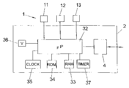
Figure 5 shows an exemplary embodiment of evaluation
electronics 2 which are formed in a separate chip,
which is applied to the device for the storage of solid
and/or liquid and/or gaseous objects and is
electrically connected to the data memory 1 of the
device via suitable contacting points (not
represented). The evaluation electronics 2 are formed,
for example, on a silicon chip. A microprocessor 32
with RAM and ROM devices 33, 34 and also a clock
generator (Clock) 35, a timer device (Timer) 37 and a
voltage supply device 36 are provided. By providing a
timer device 37, it is possible additionally to store
the time at which a compartment is mechanically changed
or the memory value of the associated memory cell 11,
12, 13 changes. The function of a timepiece is
therefore provided. When monitoring the
CA 02533462 2006-01-24
WO 2005/011564 PCT/DE2004/001668
- 14 -
state of the device, it is therefore possible also to
register the time of removal of the respective object,
such as for instance a tablet of a blister pack.
Figures 6a, 6b show a blister pack 7 with a
multiplicity of blisters 71, 72, 73 in side view and in
plan view as an example of a device for the storage of
solid and/or liquid and/or gaseous objects. Each
blister 71, 72, 73 represents part of a memory cell.
For this purpose, an interconnect 104 is respectively
integrated in the region 70 of the blister that can be
pressed in. This interconnect is destroyed when the
blister is pressed through. This leads to writing of
the memory cell assigned to the respective blister 71,
72, 73, or to a change of the memory value.
Figure 7 shows an exemplary embodiment of a memory cell
or a memory element 11. According to the exemplary
embodiment of Figure 7, a line which is partly formed
by the interconnect 104 of the compartment is connected
between the terminals Ground 102 and the operating
voltage Vdd 101. An output signal is provided at an
output 103. A p-channel transistor 100, which is
realized with preference by polymer electronics, limits
the current, so that, when the interconnect 104 is
closed, the potential at the output 103 is zero volts
(logical zero). When the interconnect 104 is
destroyed, on the other hand, the operating voltage Vdd
(logical one) is present at the output 103.
The refinement of the memory cell represented in Figure
7 is to be understood as given merely by way of
example. Numerous other refinements of a memory cell
are conceivable. For example, instead of a current-
limiting transistor, a resistor may also be provided.
For alternating current applications, capacitors and/or
inductors may also be used.
CA 02533462 2006-01-24
WO 2005/011564 PCT/DE2004/001668
- 15 -
Figure 8 shows a memory cell with six blisters 71-76
and six assigned memory cells 11-16, which are formed
for example as in Figure 7. The outputs 103 of the
memory cells are connected via electrical lines 8 to an
evaluation module 3, which reads the content from the
memory cells 71-76 and passes the data on to an
interface 4 for transmission to a reader, the
information transmission taking place for example
without contacts by means of an RFID interface.
According to the exemplary embodiment of Figure 8, not
only the memory cells 11 to 16 but also the evaluation
module 3 and the RFID module 4 are configured at least
partly by polymer electronics. Used in this case as
the carrier for the electrical lines 104, 8 is a
correspondingly structured aluminum layer of the
blister pack, which after structuring contains
interconnects in a suitable way. The further
components of the memory cells and of the evaluation
electronics 3, 4, such as transistors and diodes, are
integrated in further layers of the plastic material of
the blister pack 7. In this case it is also preferred
for the RFID interface 4 to be realized on a polymer
basis.
Instead of an RFID interface 4, an interface with
contacts, corresponding to the interface 4a of Figure
2, may also be used.
After removal of the medicament contained in the
respective blisters 71 to 76, the information on the
change of the respective blister is read into the
reading module 5 (cf. Figure 1) and presented there or
passed on. The reading module may in this case be used
with a multiplicity of blister packs of different sizes
and numbers of blisters. Commercially available RFID
readers or else readers specially designed for blister
packs may be used.
CA 02533462 2006-01-24
WO 2005/011564 PCT/DE2004/001668
- 16 -
The invention is not restricted in its implementation
to the exemplary embodiments presented above. Instead
of blister packs, any other desired packs or devices
for the storage of solid and/or liquid and/or gaseous
objects may be used in connection with the invention.
The compartments that can change mechanically when an
object is removed are, for example, compartments of
commercially available food packs. The invention then
makes it possible after a delivery of food has been
received to check quickly whether the packs of the
individual foods have been damaged during transit.
In other refinements of the invention, the filling of a
compartment is registered, an electrically readable
signal being generated when a compartment is filled.
The electrically readable signal is triggered in
particular by a mechanical change of the compartment
during the filling operation