Note: Descriptions are shown in the official language in which they were submitted.
CA 02534172 2006-O1-27
BACKGROUND OF THE INVENTION
1. Field of the Invention
The invention relates to a film having an imprinted
antenna, for use with an RFID chip. The antenna consists of a
conductor track with connector ends.
2. The Prior Art
RFID (radio frequency identification) chips are active or
passive circuits that can be read out with a reader device, in
contact-free manner, and are suitable for goods identification.
A label film having an imprinted half-wave dipole antenna is known
from International Application Publication No. WO 03/068874 A1. In
this connection, antennas having full-surface conductor tracks are
IS imprinted on the label film. The antennas are formed from a
conductor track having two conductor track pieces.
United States Patent Application Publication No.
2003/080903 A1 relates to a dipole antenna in which a plurality of
symmetrically shaped conductive structures that are spaced apart
from one another are applied to a dielectric carrier plate. Between
the structures that are spaced apart, there are additional coupling
structures that are applied separately. This antenna is used for
headsets of mobile telephones and allows a reduction of the
construction size as compared to a usual half-wave dipole antenna,
in which the length of the conductor track pieces correlates
directly with the wavelength.
-I-
CA 02534172 2006-O1-27
A tunable antenna on a flexible substrate for the high-
frequency range is known from US Patent Application Publication No.
2002/0003496 A1. The antenna has full-surface conductor tracks and
S additional, separable conductor structures for tuning the antenna.
Compared with an antenna designed for a fixed frequency, having
conductor tracks that extend proceeding from connector ends, the
production of the additional structures requires many times the
amount of conductive antenna material.
SUMMARY OF THE INVENTION
It is therefore the object of the invention to reduce the
costs and the expenditure of conductive printing ink for series
production of a film having an imprinted antenna. It is another
object of the invention to provide an antenna having good functional
properties, specifically broad bandwidth, great reflux damping, and
low transmission damping.
This object is accomplished according to the invention in
that the antenna, applied in a printing method, with a conductive
printing ink, has window-like recesses in the conductor track. The
area of the recesses amounts to at least 20% of the total area of
the conductor track having the recesses. The reference variable for
the area ratio is the total area of the conductor track including
its recesses. It is practical if the window-like recesses are
disposed so that they are essentially uniformly distributed over the
entire length of the conductor track, all the way to the connector
-2-
CA 02534172 2006-O1-27
ends. Preferably, in a top view, the conductor track has a grid
structure, which consists of two longitudinal traces that run in the
longitudinal direction of the conductor track, and a plurality of
crosspieces that connect the longitudinal traces. The grid
structure extends over the entire length of the conductor track, all
the way to the connector ends. Because of the recesses, the
material expenditure of the expensive printing ink can be
significantly reduced, without affecting the broadband radiation
properties of the antenna, compared with an antenna having a full-
area conductor track_ Broadband properties, in this connection, are
understood to be the transmission properties of the antenna above
and below the central resonance frequency of the antenna.
In order to be able to use the antenna that is applied to
the film, e.g. a label film or a packaging film, in a varied and
flexible manner when it is used with an RFID chip, a broadband value
of 100 MHz is aimed at in the UHF range between 800 and 1000 MHz or
in the SHF range between 2.4 and 2.6 GHz. The antenna preferably
has a bandwidth of more than 100 MHz, based on a reduction of the
reflux attenuation in the resonance range of up to -10 dB. The
resonance frequency of the antennas results from their geometry and
dimensions. Thus, in the case of a half-wave dipole antenna, the
length of the conductor track pieces correlates directly with the
wavelength.
Fundamentally, different printing methods can be used for
imprinting the antennas. The gravure printing method, using
-3-
CA 02534172 2006-O1-27
conductive printing ink, has proven to be particularly suitable for
series production of the film. In this connection, antennas are
imprinted on a film web using a printing ink that contains a
conductive material. In this connection, the imprinting of the
S total conductor track of an antenna takes place in one method step.
Possible film materials are polymer film material, preferably from
among the group of polyesters, polyamides, and polyolefins. These
include, for example, polyethylene terephthalate, polybutylene
terephthalate, polypropylene, polyethylene, modified or crosslinked
polyethylenes, polystyrene, and mixtures or copolymerizates of these
polymers. The films can also be coextruded in multiple layers, or
laminated.
The film web has a layer thickness between 30 and 150 Win,
1S for example. It can be brought into commerce as rolled goods. Film
sections having one antenna in each section, can be cut off from the
film web.
In addition to the high film web speeds of 50 m/min and
more, the gravure method particularly allows precise dimensioning of
the layer thickness of the conductor tracks that are applied. When
printing small structures, the gravure method, as compared with the
screen-printing method, for example, has a good edge sharpness and
low peak-to-valley height, which is less than 5 fpm. Thus, it is
2S possible to produce conductor tracks having a layer thickness below
10 Om, and tolerances of less than , 1 fIm can be adhered to for all
antennas applied to a film web. The imprinted conductor tracks have
-4-
CA 02534172 2006-O1-27
recesses having any desired irregular, in particular fractal, or
regular, preferably round, ellipsoid, or rectangular, shapes. By
reducing the imprinted area, as compared with a full-area antenna
having the same outer dimensions, the amount of printing ink used
S can be reduced, thereby clearly reducing the production costs. It
is practical if the area of the recesses amounts to more than 20%,
preferably at least 500, with reference to the total area of the
conductor track including its recesses.
By varying the width of the recesses and the thickness of
the crosspieces between the recesses, the properties of the antenna,
such as the resonance frequency, for example, can be changed in a
targeted manner.
1S BRIEF DESCRIPTION OF THE DRAWINGS
Other objects and features of the present invention will
become apparent from the following detailed description considered
in connection with the accompanying drawings. It is to be
understood, however, that the drawings are designed as an
illustration only and not as a definition of the limits of the
invention.
In the drawings, wherein similar reference characters
denote similar elements throughout the several views:
2S
Fig. 1 shows a detail from a label film web having
antennas applied using the gravure printing method;
-S-
CA 02534172 2006-O1-27
Fig. 2a - 2d show various embodiments of a half-wave
dipole antenna according to the invention;
Fig. 3 shows a half-wave dipole antenna according to the
state of the art;
Fig. 4 shows an antenna having angled conductor track
pieces; and
Fig. 5 shows an antenna loop.
DETAILED DESCRIPTION OF THE PREFERRED EMBODIMENT
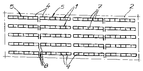
Referring now in detail to the drawings, Fig. 1 shows a
IS detail of a film web 2 imprinted with antennas 1, from which a
plurality of films 3, which are used as labels, having one antenna
1, in each instance, can be punched out. Film web 2 preferably
consists of polyethylene terephthalate (PET) and has a thickness
between 30 and 150 L-im, for example. These antennas 1 are intended
for use with RFID chips and designed for coupling in the UHF range
between 800 and 1000 MHz or in the SHF range between 2.4 and 2.6
GHz. Their conductor track 4 is divided into two conductor track
pieces 5 and forms a half-wave dipole antenna 6. Antenna 1-is
imprinted onto film web 2 using the rotation printing method, using
a conductive printing ink, and contains window-like recesses 7.
Recesses 7 form cells within the conductor track pieces 5, which are
rectangular in a top view, and have an area, in total, that is at
-6-
CA 02534172 2006-O1-27
least 20%, preferably at least 500, with reference to the outer
dimensions of antenna 1. The printing ink applied to film web 2
contains a conductive material.
The window-like recesses are essentially uniformly
distributed over the entire length of the conductor tracks, all the
way to the connector ends. In the exemplary embodiments that
represent a preferred embodiment, conductor track 4 has a grid
structure in a top view, which consists of two longitudinal traces
12 that run in the longitudinal direction of the conductor track,
and a plurality of crosspieces 9 that connect longitudinal traces
12. It is evident from the figures that the grid structure extends
over the entire length of conductor track 4, all the way to
connector ends 8.
Fig. 2a shows a film 3 that is used as a label, with an
imprinted half-wave dipole antenna 6. Half-wave dipole antenna 6
has two conductor track pieces 5 that are rectangular in a top view,
which extend to the left and the right, respectively, from a
connector end 8 for an RFID chip that is disposed in the renter.
Conductor track pieces 5 contain recesses 7 that are configured as
rectangular windows. In the embodiment of Fig. 2a, all of the
recesses 7 in conductor track pieces 5 are configured to be of a
uniform size. Crosspieces 9 between recesses 7 are part of
conductor track pieces 5 and possess the same crosspiece width in
this embodiment.
CA 02534172 2006-O1-27
In the embodiment shown in Fig. 2b, the dimensions of
recesses 7 in imprinted conductor track pieces 5 decrease in the
direction of antenna ends 10.
In the embodiment of Fig. 2c, the crosspiece width of
crosspieces 9 provided between recesses 7 changes. The crosspiece
width of these crosspieces becomes greater in the direction of
antenna ends 10.
In the embodiment of Fig. 2d, the measures described
using Fig. 2b and 2c have been combined with one another.
The half-wave dipole antennas 6 according to the
invention, presented in Fig. 2a to 2d, allow a clear reduction in
the printing ink required as compared with the corresponding state
of the art shown in Fig. 3, and thereby allow a more cost-
advantageous production of films 3 that are intended for use with an
RFID chip, with an imprinted antenna 1.
Fig. 4 shows an antenna 1 having angled conductor track
pieces. By means of this arrangement, the total length of antenna 1
can be reduced, while the antenna frequency remains the same.
Fig. 5 shows an antenna structure according to the
invention, in which the conductor track forms an antenna Loop 11.
An antenna 1 in this embodiment is also referred to as a quad-loop
or whole-wave loop, on the basis of its geometry. It has very good
_g_
CA 02534172 2006-O1-27
reception performance. Window-like recesses 11 disposed in the
conductor track can have any desired regular or irregular shape, and
are preferably round, ellipsoid, or rectangular. In this
embodiment, all the recesses 7 have essentially the same dimensions,
and crosspieces 9 have the same crosspiece width. However, recesses
7 can have different sizes, and/or the crosspieces 9 can have
different crosspiece widths.
The antennas according to the invention are characterized
by a great bandwidth, great reflex damping, as well as low
transmission damping. Surprisingly, the recesses in the conductor
track, which typically has edges that run straight, and a width that
remains uniform along its progression, cause practically no
significant transmission losses.
Accordingly, while only a few embodiments of the present
invention have been shown and described, it is obvious that many
changes and modifications may be made thereunto without departing
from the spirit and scope of the invention.
-9-