Note: Descriptions are shown in the official language in which they were submitted.
CA 02536614 2006-02-21
WO 2005/024490 PCT/N02004/000261
1
Method and device for reduction of polarization-dependent effects in a tunable
optical component
Invention
The present invention relates generally to a device and a method for reducing
polarization-dependent effects in dynamical optical components based on
surface
io modulation of a polymer gel or membrane, and specially to a device and
method that
modifies, removes or lead away unwanted reflections from incident light or
information
carrier communicating with said optical component.
Background
The high cost of components, in particular for the more advanced components
including
many subparts, is slowing down the deployment of optical communication systems
and
the introduction of all-optical networks. Consequently, it is necessary to
develop cost
effective components that have the necessary specifications, but allow low-
cost
assembly and production methods to be used.
Dynamic or tunable components are of particular demand in fiber optic
communication
systems and the modules that such systems comprise. A performing, low-cost,
and
highly scalable dynamic optical component based on surface modulation of a
polymer
gel (or membrane) is documented in the Norwegian patent application no. 2002
4265.
The state of polarization of the light in an optical communication system
fluctuates over
time due to environmental effects on the system components (especially the
optical
fiber) and changes in the topography of the system. The performance of both
the
individual components and the modules that the system is built from, should
therefore
be as independent of the polarization state of the incoming light as possible,
and change
the polarization state as little as possible. These requirements ensure
maximum
transmission distance, maximum rate of information that can be transferred,
and
maximum number of nodes that can be passed in a network.
Several optical systems have been suggested for tunable diffraction gratings
with
applications to fiber optical components. One of the known methods is
diffractive
MEMS (D-MEMS) from companies like Light Connect and Silicon Light Machines.
CA 02536614 2006-02-21
WO 2005/024490 PCT/N02004/000261
2
These devices are based on a moveable diffraction grating consisting of at
least two
separate pieces. There are provided a stationary reflective bottom surface,
and a
moveable set of thin blades, the grating, that are made of etched silicon. The
blades can
be moved up and down by the application of an appropriate electrical field.
The result is
a diffraction grating, where the effective phase shift of the grating is given
by the
relative position of the blades and the reflective surface below. This
arrangement can be
used to make effective variable optical attenuators, but the set of blades
must be
processed out of silicon. This is an expensive process, and the yield of the
process goes
dramatically down as the system size increases. Components made from D-MEMS
are
io hence effective and performing, but expensive.
US 3,527,522 disclose a light-modulating device comprising a glass prism
attached with
a reflection free glass backing plate, a transparent electrode and a
deformable material
such as silicon rubber. A substrate with addressable electrodes is arranged in
parallel
with the surface of said deformable silicon rubber with an air gap between the
material
and the substrate.
Tunable Diffraction Grating Technology
The present invention aims to have the performance of D-MEMS solutions, but
with the
same ease of manufacturing as found in LCD or LCOS methods of production. The
present invention is based on tunable surface diffraction gratings. Examples
of such
gratings have been disclosed in the literature and in patents. For example,
our preferred
embodiment is based on the arrangements described in Norwegian patent
application
no. 2002 4265.
In order to compensate for limitations caused by the materials or processes
involved in
the manufacturing and assembly, we propose a method and device according to
the
present invention that will reduce the polarization-dependent effects in
tunable
3o diffraction grating devices and systems as seen for example in the
Norwegian patent
application no. 2002 4265.
Figure Captures
Figure la and lb illustrates an example of a double pass embodiment with a
single
channel of the present invention.
CA 02536614 2006-02-21
WO 2005/024490 PCT/N02004/000261
3
Figure 2 illustrates an example of a multipass embodiment of the present
invention.
Figure 3 illustrates how reflections can provide interference effects.
Figure 4 illustrates another example of embodiment of the present invention.
Figure 5 illustrates examples of prism design according to an example of
embodiment
of the present invention.
io Figure 6 illustrates an example of a prism design according to another
example of
embodiment of the present invention.
The present invention provides minimization of the difference in effects on
orthogonal
states of polarization in the incoming light or information carrier on dynamic
optical
is components as exemplified in the Norwegian patent application no. 2002
4265, where
optical tune ability is achieved by surface modulation of a polymer gel film
or
membrane.
Double- or multipass configurations including half-waveplate
In an example of embodiment of the present invention, inserting a half-wave
plate half-
way or close to half-way in the optical path through the polymer-based or
membrane
based modulator is provided. A half-wave plate is known to a person skilled in
the art.
The effect of a half-wave plate is to rotate orthogonal polarizations 90 in
the plane
transversal to the direction of propagation. If the polarization effects in
the light path
before and after the half-waveplate are similar or close to identical,
orthogonal
polarizations will in total see the same or similar polarization effects
(polarization
dependent loss, polarization mode dispersion, etc.). The resulting effect is
that the
modulator will have no effects depending on the polarization state of the
incoming light,
3o and a minimal change in polarization state will take place.
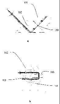
An example of such a single-pass embodiment can be found in figure la and
figure lb.
Figure 1 a illustrates an end view while figure lb illustrates a top view of
the
embodiment. There are two prisms 101 and 102 joined adjacent to one another
with a
half-wave plate 100 in between the joining prism surfaces. In figure lb the
gel surface
(or membrane) is indicated as a circle 103.
CA 02536614 2006-02-21
WO 2005/024490 PCT/N02004/000261
4
A half-wave plate 100 can be both of transmissive and reflective nature. Both
types can
be exploited in examples of embodiments of the present invention.
The light or information carrier may also hit the modulated gel (or membrane)
surface
more than twice. An example of a multiple-pass configuration with four
reflections
from the modulated gel (or membrane) surface and a half-waveplate 100 included
is
shown in figure 2.
In this example of embodiment, the distance between the diffractions is very
small and
io the Fresnel approximation is used. An interesting effect of the multiple
reflections is
that the gel amplitude can be n times lower and approximately the electrical
field can be
n times smaller while keeping a high dynamic attenuation range.
In this example of embodiment the half-wave plate is arranged inside a prism
arrangement comprising 4 different joining prism shapes 110, 111, 112 and 113
where
the prism part 112 comprises a carving for the halfwave-plate 100. The
different parts
are joined as illustrated in figure 2. A substrate 115 with electrodes
constituting the
modulating electric field is adjacent to the gel or membrane part of the
optical
component, spaced apart by the distal members 114.
Reduction or suppression of residual resonance effects
A small residual polarization effect may occur due to the non-normal incidence
of light
on the prism-polymer (or membrane) interface if the index matching between
prism and
polymer (membrane) is not sufficiently optimized.
The state of polarization of the incoming light can be decomposed into two
components,
one component parallel to (known as p-polarization) and perpendicular to
(known as s-
polarization) the plane of incidence. The plane of incidence is defined by the
incoming
3o ray direction and the perpendicular to the prism-gel (membrane) interface.
If the
difference Dn in refractive index between the gel (membrane) as indicated in
figure 3
where only a part of the complete modulator as described in the Norwegian
patent
application no. 20024265 is included. The thickness of the ITO layer applied
between
the prism end the gel (membrane) in the patent application mentioned above is
typically
only a fraction of a wavelength and has therefore less influence.
CA 02536614 2009-10-21
WO 2005/024490 PCT/N02004/000261
A standard text book gives the formulae necessary to study the polarization
effects
during reflection and refraction, see chapter 1.5, pp. 38-53 in 7th edition of
`Principles
of Optics' by Max Born and Emil Wolf, Cambridge University Press.
5 If the difference An in refractive index between the gel (membrane) and the
prism is
very small, say An=0.044 as indicated in figure 3, it can be found that for an
incident
angle of 45 , the intensity reflection coefficient RS for s-polarized light
may be roughly
10-311 while the reflectivity for p-polarized light may be roughly three
orders of
magnitude smaller.
Incoming coherent light in s-polarization with intensity 10 will experience
two major
reflections as indicated in figure 3: An intensity component Il is reflected
from the
prism-gel interface with reflection coefficient RS in the order of 10"3. A
larger
component 12 is reflected by the surface pattern on the gel set up by the
electrical field
is from the electrodes as described above. The reflective coefficient for
reflected light in
zero'th order is X.
The interference effects between I1 and I2 will result in a wavelength
dependence in the
output signal similar to what is observed in the output from the well-known
Fabry-Perot
cavity where the so-called effective free spectral range (FSR) is given by the
angle of
incidence and the gel (or membrane) thickness. The oscillations-in the
wavelength
response will have an amplitude of 2V (It I2) 2 I0 I (RS=x). For a desired
attenuation of
10 dB, the amplitude of the wavelength variations will be about 1 dB.
In other examples of embodiments according to the present invention, the so-
called
finesse of the Fabry-Perot cavity is reduced. In examples of embodiments this
is done
by:
1. Making the prism-gel (membrane) interface non-flat (scatter the reflected
light Ii)
2. Making the prism-gel (membrane) surface slightly non-parallel to the gel-
air
gap surface (or membrane-gap).
3. Introducing a curvature in one or both surfaces.
4. Introducing antireflection coating at prism-polymer (membrane) interface.
5. Modifying refractive index of either prism. Polymer (membrane) or both.
CA 02536614 2006-02-21
WO 2005/024490 PCT/N02004/000261
6
1. Partly scattering prism-gel (membrane) interface
By introducing a surface wave-front error A in the gel-prism (membrane)
interface the
reflected beam I1 will experience a wave-front phase error of A~1=2A4 and the
transmitted beam a wave-front phase error of A~2=2(nprism ngel)A4. Since the
difference
in refractive index between the gel (membrane) and prism is typically very
small,
say 0.044, the reflected beam Il will suffer a factor of 20 more from the
surface wave-
front phase error. It is therefore possibly to attenuate or scatter the
reflected beam while
only slightly perturbing the zero'th order transmitted beam. Three of the
possible
to methods according to the invention are:
1. Stop the polishing process of the prism before optical quality is reached
2. Chemical etching of polished prism surface
3. Post-scratching of already polished prism surface
2 and 3. Non-parallel or curved gel (membrane) surfaces
Non-parallel prism-gel (membrane) and gel-air (membrane) surface or a
curvature of
one or both gel (membrane) surfaces can be made during the manufacturing
process.
The effect is that the I1 component mentioned above will not be reflected in a
direction
parallel to I2, but rather spread out as a non-collimated beam.
A possible solution is to shape the gel (or membrane) during manufacturing so
that the
resulting layer is wedge-shaped in stead of having parallel surfaces. An
example is
given in figure 4. A typical range for the angle a shown in figure 4 can be
from a tenth
of a degree up to close to one degree, depending of the characteristics of the
optics at
the output of the modulator.
Non-parallel gel surfaces (membranes) can also be achieved by a modified prism
shape,
3o and by joining the modified prism to the surface of the gel (or membrane)
thereby
forming the desired non-parallel shape of the gel surface. Examples of six
possible
prism designs are shown in figure 5. The gel or membrane surface can easily be
made
flat during the manufacturing process, and it is preferable to introduce
either a slope or
some kind of a concave or a convex type of shape of the prism surface that
will be
joining the gel, and thereby forming the desired shape. The slope or convex or
concave
CA 02536614 2006-02-21
WO 2005/024490 PCT/N02004/000261
7
shape can be 1 or 2 dimensional. In a variant 1 of prism design as shown in
figure 5, a
prism 154 has a surface 150 formed with a wedge shaped section 151. A gel or
membrane adjacent surface is indicated by the dotted line 153. Variant 2 in
figure 5
illustrates that the slope of the wedge shaped section can be in any desired
direction
relative to the prism surface 150. Variant 3,4, 5 and 6 illustrates how a
wedge shaped
section can be forms as a carving on the surface 150 of the prism 154.
In yet another example of embodiment of the present invention, both a wedge
shaped
section and a half-wave plate is provided in one and same optical component.
io 4. Introducing antireflection coating at prism-pol finer (membrane)
interface
In one embodiment, one or several additional layer or layers (normally
referred to as an
anti-reflection coating or AR-coating) can be added between the surface of the
prism
and the ITO-layer that is next to the polymer film, see figure 6. The
thickness of the
is ITO layer is typically only a fraction of a wavelength and has therefore
less influence.
The AR coating is designed so that its refractive index is in the range
between the
refractive indices of the prism and the polymer film (membrane). This will
reduce the
effective reflectivity seen by s- and p-polarized light when leaving the prism
and
entering the polymer film. The intensity of the ray labeled Il will be lowered
compared
20 to the case when there is no AR coating present.
In yet another embodiment the refractive index of the ITO-layer could be
modified in
order to serve as an AR coating or a material that could act both as a bias
electrode and
an AR-coating could be used in stead of the ITO.
5. Modifying refractive index of either prism, polymer (membrane) or both
The difference in the refractive indices of the prism and the polymer
(membrane) may
be reduced by modifying one or both of the indices. This can be done by adding
suitable
3o dopants to the respective materials during manufacturing.