Language selection

Search

Patent 2536624 Summary

Third-party information liability

Some of the information on this Web page has been provided by external sources. The Government of Canada is not responsible for the accuracy, reliability or currency of the information supplied by external sources. Users wishing to rely upon this information should consult directly with the source of the information. Content provided by external sources is not subject to official languages, privacy and accessibility requirements.

Claims and Abstract availability

Any discrepancies in the text and image of the Claims and Abstract are due to differing posting times. Text of the Claims and Abstract are posted:

  • At the time the application is open to public inspection;
  • At the time of issue of the patent (grant).
(12) Patent: (11) CA 2536624
(54) English Title: PROGRAMMABLE LOGIC DEVICE INCLUDING PROGRAMMABLE MULTI-GIGABIT TRANSCEIVERS
(54) French Title: LOGIQUE PROGRAMMABLE COMPRENANT DES EMETTEURS-RECEPTEURS PROGRAMMABLES A PLUSIEURS GIGABITS
Status: Granted and Issued
Bibliographic Data
(51) International Patent Classification (IPC):
  • H04L 25/14 (2006.01)
  • G06F 15/76 (2006.01)
  • H03K 19/177 (2020.01)
  • H04B 01/40 (2015.01)
  • H04L 09/18 (2006.01)
(72) Inventors :
  • GROEN, ERIC D. (United States of America)
  • BOECKER, CHARLES W. (United States of America)
  • BLACK, WILLIAM C. (United States of America)
  • IRWIN, SCOTT A. (United States of America)
  • KRYZAK, JOSEPH N. (United States of America)
  • CHEN, YIQIN (United States of America)
  • JENKINS, ANDREW G. (United States of America)
  • HOELSCHER, AARON J. (United States of America)
(73) Owners :
  • XILINX, INC.
(71) Applicants :
  • XILINX, INC. (United States of America)
(74) Agent: SMITHS IP
(74) Associate agent:
(45) Issued: 2009-06-02
(86) PCT Filing Date: 2004-09-10
(87) Open to Public Inspection: 2005-03-24
Examination requested: 2008-11-04
Availability of licence: N/A
Dedicated to the Public: N/A
(25) Language of filing: English

Patent Cooperation Treaty (PCT): Yes
(86) PCT Filing Number: PCT/US2004/029864
(87) International Publication Number: US2004029864
(85) National Entry: 2006-02-22

(30) Application Priority Data:
Application No. Country/Territory Date
10/661,016 (United States of America) 2003-09-11

Abstracts

English Abstract


A programmable logic device includes a plurality of programmable multi-gigabit
transceivers, programmable logic fabric, and a control module. Each of the
plurality of programmable multi-gigabit transceivers is individually
programmed to a desired transceiving mode of operation in accordance with a
plurality of transceiver settings. The programmable logic fabric is operably
coupled to the plurality of programmable multi-gigabit transceivers and is
configured to process at least a portion of the data being transceived via the
multi-gigabit transceivers. The control module is operably coupled to produce
the plurality of transceiver settings based on a desired mode of operation for
the programmable logic device.


French Abstract

L'invention porte sur un dispositif à logique programmable comprenant une pluralité d'émetteurs-récepteurs programmables à plusieurs gigabits, un réseau logique programmable et un module de commande. Chaque pluralité de la pluralité d'émetteurs-récepteurs programmables à plusieurs gigabits est programmée individuellement selon un mode d'exploitation en émission-réception désiré, conformément à une pluralité de paramétrages des émetteurs-récepteurs. Le réseau logique programmable est couplé de manière fonctionnelle à la pluralité d'émetteurs-récepteurs programmables à plusieurs gigabits et est configuré pour traiter en émission-réception au moins une partie des données. Le module de commande est couplé de manière fonctionnelle pour produire la pluralité de paramétrages en émission-réception en tenant compte d'un mode de fonctionnement voulu du dispositif à logique programmable.

Claims

Note: Claims are shown in the official language in which they were submitted.


What is claimed is:
1. A programmable multi-gigabit transceiver comprises:
programmable physical media attachment (PMA) module operably coupled to
convert transmit parallel data into transmit serial data in accordance with a
programmed serialization setting and to convert receive serial data into
receive
parallel data in accordance with a programmed deserialization setting;
programmable physical coding sublayer (PCS) module operably coupled to
convert transmit data words into the transmit parallel data in accordance with
a
transmit interface setting and to convert the receive parallel data into
receive
data words in accordance with a receive interface setting, the PCS module
comprising:
a programmable PCS receive module operably coupled to convert the
receive parallel data into receive data words in accordance with the receive
interface setting, the receive module comprising:
a programmable data alignment module operably coupled to align the
receive parallel data in accordance with the receive interface setting to
produce aligned data words, wherein size and rate of the aligned data
words are set based on the receive interface setting;
a programmable descramble and decode module operably coupled to
descramble, decode, or pass the aligned data words in accordance with
the receive interface setting to produce processed aligned data words,
wherein the receive interface setting indicates descrambling, decoding,
or passing of the aligned data words, wherein the receive interface
27

setting further indicates a type of descrambling when the programmable
descramble and decode module is descrambling the aligned data words
and further indicates a type of decoding when the programmable
descramble and decode module is decoding the aligned data words;
a programmable storage module operably coupled to elastic store or
pass the processed data words in accordance with the receive interface
setting to produce stored data words; and
a programmable decode and verify module operably coupled to decode,
verify or pass the stored data words in accordance with the receive
interface setting and the programmed logic interface setting to produce
the receive data words, wherein the receive interface setting indicates
the decoding, the verifying or the passing of the stored data words,
indicates a second type of decoding when the programmable decode and
verify module is decoding the stored data words and indicates a type of
verifying when the programmable decode and verify module is
verifying the stored data words and wherein the programmed logic
interface setting indicates rate and size of the received data words;
programmable interface operably to convey the receive data words from the
programmable PCS module to a programmable logic fabric section and to
convey the transmit data words from the programmable logic fabric section to
the programmable PCS module in accordance with a programmed logic
interface setting; and
control module operably coupled to generate the programmed serialization
setting, the programmed deserialization setting, the receive interface
setting,
28

the transmit interface setting, and the logic interface setting based on a
desired
mode of operation for the programmable multi-gigabit transceiver.
2. The programmable multi-gigabit transceiver of claim 1, wherein the
programmable PMA further comprises:
a programmable PMA receiver module operably coupled to deserialize the
receive serial data in accordance with the programmed deserialization selling
to produce the receive parallel data; and
a programmable PMA transmitter module operably coupled to serialize the
transmit parallel data in accordance with a programmed serialization setting
to
produce the transmit serial data.
3. The programmable multi-gigabit transceiver of claim 2, wherein the
programmable PMA receiver module further comprises:
programmable analog front-end operably coupled to amplify and equalize the
receive serial data to produce amplified and equalized receive serial data,
wherein amplification and equalization performed by the programmable analog
front-end are set in accordance with the programmed deserialization setting;
data and clock recovery module operably coupled to recover data and a clock
from the amplified and equalized receive serial data to produce recovered data
and a recovered clock, respectively, wherein the data and clock recovery
module includes a programmable phase locked loop that is programmed in
accordance with the programmed deserialization setting; and
29

serial-to-parallel module operably coupled to convert the recovered data into
the receive parallel data, wherein rate of the receive parallel data and width
of
the receive parallel data are set in accordance with the programmed
deserialization setting.
4. The programmable multi-gigabit transceiver of claim 2, wherein the
programmable PMA transmitter module further comprises:
phase locked loop operably coupled to produce timing signals in accordance
with the programmed serialization selling;
parallel-to-serial module operably coupled to convert the transmit parallel
data
into the transmit serial data based on the timing signals, wherein data width
of
the transmit parallel data and rate of the transmit serial data are set in
accordance with the programmed serialization setting; and
driver operably coupled to drive the transmit serial data on to a transmission
line, wherein drive level of the driver and pre-emphasis settings of the
driver is
set in accordance with the programmed serialization setting.
5. The programmable multi-gigabit transceiver of claim 1, wherein the
programmable PCS module further comprises:
a programmable PCS transmit module operably coupled to convert the transmit
data words into the transmit parallel data in accordance with the transmit
interface setting.
6. The programmable multi-gigabit transceiver of claim 5, wherein the
programmable PCS transmit module further comprises:

programmable verify module operably coupled to verify or pass the transmit
data words in accordance with the transmit interface setting and the
programmed logic interface setting to produce verified transmit data words and
wherein the programmed logic interface setting indicates size and rate of the
transmit data words;
programmable encoding module operably coupled to encode or pass the
verified transmit data words in accordance with the transmit interface setting
to
produce encoded data words, wherein the transmit interface setting indicates a
type of encoding when the programmable encoding module is encoding the
verified transmit data words;
programmable storage module operably coupled to elastic store or pass the
encoded data words in accordance with the transmit interface setting to
produce stored encoded data words; and
programmable scrambling module operably coupled to scramble or pass the
stored encoded data words in accordance with the transmit interface setting to
produce the transmit parallel data, wherein the transmit interface setting
indicates a type of scrambling when the programmable scrambling module is
scrambling the stored encoded data words.
7. The programmable multi-gigabit transceiver of claim 1 further comprises:
a PMA memory mapped register operable to store element settings for
elements of the PMA module as indicated by the programmed serialization
setting and the programmed deserialization setting; and
31

PCS register operable to store element settings for elements of the PCS module
as indicated by the transmit and receive interface settings and the programmed
logic interface setting.
8. The programmable multi-gigabit transceiver of claim 7, wherein the control
module further functions to:
receive a programming setting that indicates the desired mode of operation for
the programmable multi-gigabit transceiver;
convert the programming setting into the programmed serialization setting, the
programmed deserialization setting, the receive interface setting, the
transmit
interface setting, and the logic interface setting;
provide the programmed serialization setting and the programmed
deserialization setting to the PMA memory mapped register; and
provide the transmit and receive interface settings and the programmed logic
interface setting to the PCS register.
9. The programmable multi-gigabit transceiver of claim 7, wherein the control
module further functions to:
determine a programming setting that indicates the desired mode of operation
for the programmable multi-gigabit transceiver based on auto-configuration
information;
32

convert the programming setting into the programmed serialization setting, the
programmed deserialization setting, the receive interface setting, the
transmit
interface setting, and the logic interface setting;
provide the programmed serialization setting and the programmed
deserialization setting to the PMA memory mapped register; and
provide the transmit and receive interface settings and the programmed logic
interface setting to the PCS register.
10. The programmable multi-gigabit transceiver of claim 1, wherein the control
module further functions to:
generate the programmed serialization setting to enable, logically disable, or
physically disable at least one element of a programmable PMA receiver
module of the programmable PMA module;
generate the programmed deserialization setting to enable, logically disable,
or
physically disable at least one element of a programmable PMA transmit
module of the programmable PMA module;
generate the transmit interface setting to enable, logically disable, or
physically
disable at least one element of a programmable PCS transmit module of the
programmable PCS module; and
generate the receive interface setting to enable, logically disable, or
physically
disable at least one element of a programmable PCS receive module of the
programmable PCS module.
33

11. A programmable logic device comprises:
clock management module operably coupled to provide a reference clock from
one of a plurality of clock sources;
transmit physical media attachment (PMA) module operably coupled to
convert parallel transmit data into serial transmit data, wherein the transmit
PMA module receives the parallel transmit data in accordance with a parallel
transmit clock and transmits the serial transmit data in accordance with a
serial
transmit clock, wherein the transmit PMA module generates the parallel
transmit clock, the serial transmit clock, and a transmit programmable logic
clock based on the reference clock;
receive PMA module operably coupled to convert serial receive data into
parallel receive data, wherein the receive PMA module receives the serial
receive data in accordance with a serial receive clock and provides the
parallel
receive data in accordance with a parallel receive clock, wherein the receive
PMA module generates the serial receive clock, the parallel receive clock, and
a receive programmable logic clock based on the reference clock;
transmit physical coding sublayer (PCS) module operably coupled to convert
transmit data words into the parallel transmit data in accordance with the
parallel transmit clock;
receive PCS module operably coupled to convert the parallel receive data into
receive data words in accordance with the parallel receive clock;
programmable logic fabric operably coupled to produce the transmit data
words in accordance with the transmit programmable logic clock and to
34

process the received data words in accordance with the receive programmable
logic clock;
wherein the plurality of clock source further comprises a low jitter external
clock source, a recovered clock, and internal clock of the programmable logic
fabric; and
wherein the receive PCS module further comprises:
programmable data alignment module operably coupled to align data words
of the parallel receive data in accordance with a receive interface setting
and the parallel transmit clock to produce aligned data words wherein size
and rate of the aligned data words are set based on the receive interface
setting;
programmable descramble and decode module operably coupled to
descramble, decode, or pass the aligned data words in accordance with the
receive interface setting to produce processed aligned data words, wherein
the receive interface setting indicates descrambling, decoding, or passing of
the aligned data words, wherein the receive interface setting further
indicates a type of descrambling when the programmable descramble and
decode module is descrambling the aligned data words and further indicates
a type of decoding when the programmable descramble and decode module
is decoding the aligned data words;
programmable storage module operably coupled to elastic store or pass the
processed data words in accordance with the receive interface setting to
produce stored data words; and

programmable decode and verify module operably coupled to decode,
verify or pass the stored data words in accordance with the receive interface
setting and a programmed logic interface setting to produce the receive data
words, wherein the receive interface setting indicates the decoding, the
verifying or the passing of the stored data words, indicates a second type of
decoding when the programmable decode and verify module is decoding
the stored data words and indicates a type of verifying when the
programmable decode and verify module is verifying the stored data words
and wherein the programmed logic interface setting indicates rate and size
of the received data words.
12. The programmable logic device of claim 11, wherein the reference clock
further
comprises:
a transmit reference clock that is provided to the transmit PMA module,
wherein the transmit PMA, module generates the serial transmit clock and the
parallel transmit clock based on the transmit reference clock; and
a receive reference clock that is provided to the receive PMA module, wherein
the receive PMA module generates the serial receive clock and the parallel
receive clock based on the receive reference clock.
13. The programmable logic device of claim 11, wherein the receive PMA module
further comprises:
programmable analog front-end operably coupled to amplify and equalize the
serial receive data to produce amplified and equalized serial receive data,
wherein amplification and equalization performed by the programmable analog
front-end are set in accordance with a programmed deserialization setting;
36

data and clock recovery module operably coupled to recover data and a clock
from the amplified and equalized serial receive data to produce recovered data
and a recovered clock, respectively, wherein the data and clock recovery
module includes a programmable phase locked loop that is programmed in
accordance with the programmed deserialization setting, wherein the phase
locked loop generates the serial receive clock, parallel receive clock, and
the
receive programmable logic clock based on the recovered clock and the
reference clock; and
serial-to-parallel module operably coupled to convert the recovered data into
the parallel receive data, wherein rate of the parallel receive data and width
of
the parallel receive data are set in accordance with the programmed
deserialization setting.
14. The programmable logic device of claim 11, wherein the transmit PMA module
further comprises:
phase locked loop operably coupled to produce the serial transmit clock, the
parallel transmit clock, and the transmit programmable logic clock based on
the reference clock in accordance with a programmed serialization setting;
parallel-to-serial module operably coupled to convert the parallel transmit
data
into a serial data stream based on the serial transmit clock and the parallel
transmit clock, wherein data width of the parallel transmit data and rate of
the
serial data stream are set in accordance with the programmed serialization
setting; and
37

driver operably coupled to drive the serial data stream on to a transmission
line
as the serial transmit data, wherein drive level of the driver and pre-
emphasis
settings of the driver is set in accordance with the programmed serialization
setting.
15. The programmable logic device of claim 11, wherein the transmit PCS module
further comprises:
programmable verify module operably coupled to verity or pass the transmit
data words in accordance with a transmit interface setting and a programmed
logic interface setting to produce verified transmit data words and wherein
the
programmed logic interface setting indicates size and rate of the transmit
data
words;
programmable encoding module operably coupled to encode or pass the
verified transmit data words in accordance with the transmit interface setting
to
produce encoded data words, wherein the transmit interface setting indicates a
type of encoding when the programmable encoding module is encoding the
verified transmit data words;
programmable storage module operably coupled to elastic store or pass the
encoded data words in accordance with the transmit interface setting to
produce stored encoded data words; and
programmable scrambling module operably coupled to scramble or pass the
stored encoded data words in accordance with the transmit interface setting to
produce the parallel transmit data, wherein the transmit interface setting
indicates a type of scrambling when the programmable scrambling module is
scrambling the stored encoded data words.
38

16. A programmable multi-gigabit transceiver comprises:
a transmit section operably coupled to convert transmit data words into
transmit serial data in accordance with a transmit setting;
a receive section operably coupled to convert receive serial data stream into
receive data words in accordance with a receive setting;
an interface to programmable logic section operably coupled to provide the
transmit data words from the programmable logic section to the transmit
section in accordance with the transmit setting and to receive the receive
data
words from the receive section in accordance with the receive setting; and
control module operably coupled to produce the transmit setting and the
receive setting based on transceiver operational requirements;
wherein the control module further functions to:
generate the receive setting to enable, logically disable, or physically
disable at
least one element of a programmable PMA receiver module of the receiver
section;
generate the transmit setting to enable, logically disable, or physically
disable
at least one element of a programmable PMA transmit module of the transmit
section;
39

generate the transmit setting to enable, logically disable, or physically
disable
at least one element of a programmable PCS transmit module of the transmit
section; and
generate the receive setting to enable, logically disable, or physically
disable at
least one element of a programmable PCS receive module of the receive
section;
wherein the receive section further comprises:
a programmable physical media attachment (PMA) receive module operably
coupled to convert the receive serial data into receive parallel data in
accordance with the receive setting; and a programmable physical coding
sublayer (PCS) receive module operably coupled to convert the receive parallel
data into the receive data words in accordance with the receive setting; and
wherein the programmable PCS receive module further comprises:
programmable data alignment module operably coupled to align the receive
parallel data in accordance with the receive setting to produce aligned data
words, wherein size and rate of the aligned data words are set based on the
receive setting;
programmable descramble and decode module operably coupled to
descramble, decode, or pass the aligned data words in accordance with the
receive setting to produce processed aligned data words, wherein the receive
setting indicates descrambling, decoding, or passing of the aligned data
words,
wherein the receive setting further indicates a type of descrambling when the
programmable descramble and decode module is descrambling the aligned data

words and further indicates a type of decoding when the programmable
descramble and decode module is decoding the aligned data words;
programmable storage module operably coupled to elastic store or pass the
processed data words in accordance with the receive setting to produce stored
data words; and
programmable decode and verify module operably coupled to decode, verify or
pass the stored data words in accordance with the receive setting and the
programmed logic interface setting to produce the receive data words, wherein
the receive setting indicates the decoding, the verifying or the passing of
the
stored data words, indicates a second type of decoding when the programmable
decode and verify module is decoding the stored data words and indicates a
type of verifying when the programmable decode and verify module is
verifying the stored data words and wherein the programmed logic interface
setting indicates rate and size of the received data words.
17. The programmable multi-gigabit transceiver of claim 16, wherein the
transmit
section further comprises:
a programmable physical coding sublayer (PCS) transmit module operably
coupled to convert the transmit data words into transmit parallel data in
accordance with the transmit setting; and
a programmable physical media attachment (PMA) transmit module operably
coupled to serialize the transmit parallel data in accordance with the
transmit
setting to produce the transmit serial data.
18. The programmable multi-gigabit transceiver of claim 17, wherein the
programmable PMA transmit module further comprises:
41

phase locked loop operably coupled to produce timing signals in accordance
with the transmit setting;
parallel-to-serial module operably coupled to convert the transmit parallel
data
into the transmit serial data based on the transmit setting, wherein data
width of
the transmit parallel data and rate of the transmit serial data are set in
accordance with the transmit setting; and
driver operably coupled to drive the transmit serial data on to a transmission
line, wherein drive level of the driver and pre-emphasis settings of the
driver is
set in accordance with the transmit setting.
19. The programmable multi-gigabit transceiver of claim 17, wherein the
programmable PCS transmit module further comprises:
programmable verify module operably coupled to verify or pass the transmit
data words in accordance with the transmit setting to produce verified
transmit
data words and wherein the transmit setting indicates size and rate of the
transmit data words;
programmable encoding module operably coupled to encode or pass the
verified transmit data words in accordance with the transmit setting to
produce
encoded data words, wherein the transmit setting indicates a type of encoding
when the programmable encoding module is encoding the verified transmit
data words;
42

programmable storage module operably coupled to elastic store or pass the
encoded data words in accordance with the transmit setting to produce stored
encoded data words; and
programmable scrambling module operably coupled to scramble or pass the
stored encoded data words in accordance with the transmit setting to produce
the transmit parallel data, wherein the transmit setting indicates a type of
scrambling when the programmable scrambling module is scrambling the
stored encoded data words.
20. The programmable multi-gigabit transceiver of claim 16, wherein the
programmable PMA receive module further comprises:
programmable analog front-end operably coupled to amplify and equalize the
receive serial data to produce amplified and equalized receive serial data,
wherein amplification and equalization performed by the programmable analog
front-end are set in accordance with the receive setting;
data and clock recovery module operably coupled to recover data and a clock
from the amplified and equalized receive serial data to produce recovered data
and a recovered clock, respectively, wherein the data and clock recovery
module includes a programmable phase locked loop that is programmed in
accordance with the receive setting; and
serial-to-parallel module operably coupled to convert the recovered data into
the receive parallel data, wherein rate of the receive parallel data and width
of
the receive parallel data are set in accordance with the receive setting.
43

21. The programmable multi-gigabit transceiver of claim 16, wherein the
control
module further functions to:
receive a programming setting that indicates the desired mode of operation for
the programmable multi-gigabit transceiver; and
convert the programming setting into the receive setting and the transmit
setting.
22. A programmable logic device comprises:
a plurality of programmable multi-gigabit transceivers, wherein each of the
plurality of programmable multi-gigabit transceivers is individually
programmed to a desired transceiving mode of operation in accordance with a
plurality of transceiver settings to transceive data;
programmable logic fabric operably coupled to the plurality of programmable
multi-gigabit transceivers, wherein the programmable logic fabric is
configured to process at least a portion of the data;
control module operably coupled to produce the plurality of transceiver
settings based on a desired mode of operation of the programmable logic
device;
wherein each of the plurality of programmable multi-giga bit transceivers
further comprises:
programmable physical media attachment (PMA) module operably coupled
to transmit parallel data into transmit serial data in accordance with a
44

programmed serialization setting of a corresponding one of the plurality of
transceiver settings and to convert receive serial data into receive parallel
data in accordance with a programmed deserialization setting of the
corresponding one of the plurality of transceiver settings;
programmable physical coding sublayer (PCS) module operably coupled to
convert transmit data words into the transmit parallel data in accordance
with a transmit PMA PCS interface setting of the corresponding one of the
plurality of transceiver settings and to convert the receive parallel data
into
receive data words in accordance with a receive PMA PCS interface setting
of the corresponding one of the plurality of transceiver settings; and
programmable interface operably to convey the receive data words from the
programmable PCS module to the programmable logic fabric section and
the convey the transmit data words from the programmable logic fabric
section to the programmable PCS module in accordance with a
programmed logic interface setting, wherein the control module generates
the programmed serialization setting, the programmed deserialization
setting, the receive PMA PCS interface setting, the transmit PMA PCS
interface setting, and the logic interface setting based on a desired mode of
operation for the programmable multi-gigabit transceiver;
wherein the programmable PCS module further comprises:
a programmable PCS receive module operably coupled to convert the
receive parallel data into the receive data words in accordance with the
receive PMA PCS interface setting; and
45

a programmable PCS transmit module operably coupled to convert the
transmit data words into the transmit parallel data in accordance with the
transmit PMA PCS interface setting; and
wherein the programmable PCS receive module further comprises:
programmable data alignment module operably coupled to align the receive
parallel data in accordance with the receive PMA PCS interface setting to
produce aligned data words, wherein size and rate of the aligned data words
are set based on the receive PMA PCS interface setting;
programmable descramble and decode module operably coupled to
descramble, decode, or pass the aligned data words in accordance with the
receive PMA PCS interface setting to produce processed aligned data
words, wherein the receive PMA PCS interface setting indicates
descrambling, decoding, or passing of the aligned data words, wherein the
receive PMA PCS interface setting further indicates a type of descrambling
when the programmable descramble and decode module is descrambling
the aligned data words and further indicates a type of decoding when the
programmable descramble and decode module is decoding the aligned data
words;
programmable storage module operably coupled to elastic store or pass the
processed data words in accordance with the receive PMA PCS interface
setting to produce stored data words; and
programmable decode and verity module operably coupled to decode,
verify or pass the stored data words in accordance with the receive PMA
PCS interface setting and the programmed logic interface setting to produce
46

the receive data words, wherein the receive PMA PCS interface setting
indicates the decoding, the verifying or the passing of the stored data
words, indicates a second type of decoding when the programmable decode
and verity module is decoding the stored data words and indicates a type of
verifying when the programmable decode and verify module is verifying
the stored data words and wherein the programmed logic interface setting
indicates rate and size of the received data words.
23. The programmable logic device of claim 22, wherein the programmable PMA
further comprises:
a programmable PMA receiver module operably coupled to convert the receive
serial data into the receive parallel data in accordance with the programmed
deserialization setting; and
a programmable PMA transmitter module operably coupled to convert the
transmit parallel data into the transmit serial data in accordance with a
programmed serialization setting.
24. The programmable logic device of claim 23, wherein the programmable PMA
receiver module further comprises:
programmable analog front-end operably coupled to amplify and equalize the
receive serial data to produce amplified and equalized receive serial data,
wherein amplification and equalization performed by the programmable analog
front-end are set in accordance with the programmed deserialization setting;
data and clock recovery module operably coupled to recover data and a clock
from the amplified and equalized receive serial data to produce recovered data
47

and a recovered clock, respectively, wherein the data and clock recovery
module includes a programmable phase locked loop that is programmed in
accordance with the programmed deserialization setting; and
serial-to-parallel module operably coupled to convert the recovered data into
the receive parallel data, wherein rate of the receive parallel data and width
of
the receive parallel data are set in accordance with the programmed
deserialization setting.
25. The programmable logic device of claim 23, wherein the programmable PMA
transmitter module further comprises:
phase locked loop operably coupled to produce timing signals in accordance
with the programmed serialization setting;
parallel-to-serial module operably coupled to convert the transmit parallel
data
into the transmit serial data based on the timing signals, wherein data width
of
the transmit parallel data and rate of the transmit serial data are set in
accordance with the programmed serialization setting; and
driver operably coupled to drive the transmit serial data on to a transmission
line, wherein drive level of the driver and pre-emphasis settings of the
driver is
set in accordance with the programmed serialization setting.
26. The programmable logic device of claim 22, wherein the programmable PCS
transmit module further comprises:
programmable verify module operably coupled to verify or pass the transmit
data words in accordance with the transmit PMA_PCS interface setting and the
48

programmed logic interface setting to produce verified transmit data words and
wherein the programmed logic interface setting indicates size and rate of the
transmit data words;
programmable encoding module operably coupled to encode or pass the
verified transmit data words in accordance with the transmit PMA_PCS
interface setting to produce encoded data words, wherein the transmit
PMA_PCS interface setting indicates a type of encoding when the
programmable encoding module is encoding the verified transmit data words;
programmable storage module operably coupled to elastic store or pass the
encoded data words in accordance with the transmit PMA_PCS interface
setting to produce stored encoded data words; and
programmable scrambling module operably coupled to scramble or pass the
stored encoded data words in accordance with the transmit PMA_PCS
interface setting to produce the transmit parallel data, wherein the transmit
PMA_PCS interface setting indicates a type of scrambling when the
programmable scrambling module is scrambling the stored encoded data
words.
27. The programmable logic device of claim 22, wherein each of the
programmable
multi-gigabit transceivers further comprises:
a PMA memory mapped register operable to store element settings for
elements of the PMA module as indicated by the programmed serialization
setting and the programmed deserialization setting; and
49

PCS register operable to store element settings for elements of the PCS module
as indicated by the transmit and receive PMA_PCS interface settings and the
programmed logic interface setting.
28. The programmable logic device of claim 27, wherein the control module
further
functions to:
receive a programming setting that indicates the desired mode of operation for
the programmable multi-gigabit transceiver;
convert the programming setting into the programmed serialization setting, the
programmed deserialization setting, the receive PMA_PCS interface setting,
the transmit PMA_PCS interface setting, and the logic interface setting;
provide the programmed serialization setting and the programmed
deserialization setting to the PMA memory mapped register; and
provide the transmit and receive PMA_PCS interface settings and the
programmed logic interface setting to the PCS register.
29. The programmable logic device of claim 27, wherein the control module
further
functions to:
determine a programming setting that indicates the desired mode of operation
for the programmable multi-gigabit transceiver based on auto-configuration
information;
50

convert the programming setting into the programmed serialization setting, the
programmed deserialization setting, the receive PMA_PCS interface setting,
the transmit PMA_PCS interface setting, and the logic interface setting;
provide the programmed serialization setting and the programmed
deserialization setting to the PMA memory mapped register; and
provide the transmit and receive PMA_PCS interface settings and the
programmed logic interface setting to the PCS register.
30. The programmable logic device of claim 22, wherein the control module
further
functions to:
generate the programmed serialization setting to enable, logically disable, or
physically disable at least one element of a programmable PMA receiver
module of the programmable PMA module;
generate the programmed deserialization setting to enable, logically disable,
or
physically disable at least one element of a programmable PMA transceiver
module of the programmable PMA module;
generate the transmit PMA_PCS interface setting to enable, logically disable,
or physically disable at least one element of a programmable PCS transmit
module of the programmable PCS module; and
generate the receive PMA_PCS interface setting to enable, logically disable,
or
physically disable at least one element of a programmable PCS receive module
of the programmable PCS module.
51

31. The programmable logic device of claim 22, wherein each of the plurality
of
programmable multi-gigabit transceivers further comprises:
a transmit section operably coupled to convert transmit data words into an
transmit serial data in accordance with a transmit setting;
a receive section operably coupled to convert receive serial data stream into
receive data words in accordance with a receive setting;
an interface to programmable logic fabric operably coupled to provide the
transmit data words from the programmable logic fabric to the transmit section
in accordance with the transmit setting and to provide the receive data words
from the receive section to the programmable logic fabric in accordance with
the receive setting; and
control module operably coupled to produce the transmit setting and the
receive setting based on transceiver operational requirements.
32. The programmable logic device of claim 31, wherein the transmit section
further
comprises:
a programmable physical coding sublayer (PCS) transmit module operably
coupled to convert the transmit data words into transmit parallel data in
accordance with the transmit setting; and
a programmable physical media attachment (PMA) transmit module operably
coupled to serialize the transmit parallel data in accordance with the
transmit
setting to produce the transmit serial data.
52

33. The programmable logic device of claim 32, wherein the programmable PMA
transmit module further comprises:
phase locked loop operably coupled to produce timing signals in accordance
with the transmit setting;
parallel-to-serial module operably coupled to convert the transmit parallel
data
into the receive serial data based on the transmit setting, wherein data width
of
the transmit parallel data and rate of the transmit serial data are set in
accordance with the transmit setting; and
driver operably coupled to drive the transmit serial data on to a transmission
line, wherein drive level of the driver and pre-emphasis settings of the
driver is
set in accordance with the transmit setting.
34. The programmable logic device of claim 32, wherein the programmable PCS
transmit module further comprises:
programmable verify module operably coupled to verify or pass the transmit
data words in accordance with the transmit setting to produce verified
transmit
data words and wherein the transmit setting indicates size and rate of the
transmit data words;
programmable encoding module operably coupled to encode or pass the
verified transmit data words in accordance with the transmit setting to
produce
encoded data words, wherein the transmit setting indicates a type of encoding
when the programmable encoding module is encoding the verified transmit
data words;
53

programmable storage module operably coupled to elastic store or pass the
encoded data words in accordance with the transmit setting to produce stored
encoded data words; and
programmable scrambling module operably coupled to scramble or pass the
stored encoded data words in accordance with the transmit setting to produce
the transmit parallel data, wherein the transmit setting indicates a type of
scrambling when the programmable scrambling module is scrambling the
stored encoded data words.
35. The programmable logic device of claim 31, wherein the receive section
further
comprises:
a programmable physical media attachment (PMA) receive module operably
coupled to convert the receive serial data into receive parallel data in
accordance with the receive setting; and
a programmable physical coding sublayer (PCS) receive module operably
coupled to convert the receive parallel data into the receive data words in
accordance with the receive setting.
36. The programmable logic device of claim 35, wherein the programmable PMA
receive module further comprises:
programmable analog front-end operably coupled to amplify and equalize the
receive serial data to produce amplified and equalized receive serial data,
wherein amplification and equalization performed by the programmable analog
front-end are set in accordance with the receive setting;
54

data and clock recovery module operably coupled to recover data and a clock
from the amplified and equalized high-speed receive serial data to produce
recovered data and a recovered clock, respectively, wherein the data and clock
recovery module includes a programmable phase locked loop that is
programmed in accordance with the receive setting; and
serial-to-parallel module operably coupled to convert the recovered data into
the receive parallel data, wherein rate of the receive parallel data and width
of
the receive parallel data are set in accordance with the receive setting.
37. The programmable logic device of claim 35, wherein the programmable PCS
receive module further comprises:
programmable data alignment module operably coupled to align the receive
parallel data in accordance with the receive setting to produce aligned data
words, wherein size and rate of the aligned data words are set based on the
receive setting;
programmable descramble and decode module operably coupled to
descramble, decode, or pass the aligned data words in accordance with the
receive setting to produce processed aligned data words, wherein the receive
setting indicates descrambling, decoding, or passing of the aligned data
words,
wherein the receive setting further indicates a type of descrambling when the
programmable descramble and decode module is descrambling the aligned data
words and further indicates a type of decoding when the programmable
descramble and decode module is decoding the aligned data words;

programmable storage module operably coupled to elastic store or pass the
processed data words in accordance with the receive setting to produce stored
data words; and
programmable decode and verify module operably coupled to decode, verify or
pass the stored data words in accordance with the receive setting and the
programmed logic interface setting to produce the receive data words, wherein
the receive setting indicates the decoding, the verifying or the passing of
the
stored data words, indicates a second type of decoding when the programmable
decode and verify module is decoding the stored data words and indicates a
type of verifying when the programmable decode and verify module is
verifying the stored data words and wherein the programmed logic interface
setting indicates rate and size of the received data words.
38. The programmable logic device of claim 31, wherein the control module
further
functions to:
receive a programming setting that indicates the desired mode of operation for
the programmable multi-gigabit transceiver; and
convert the programming setting into the receive setting and the transmit
setting.
39. The programmable logic device of claim 31, wherein the control module
further
functions to:
generate the receive setting to enable, logically disable, or physically
disable at
least one element of a programmable PMA receiver module of the receiver
section;
56

generate the transmit setting to enable, logically disable, or physically
disable
at least one element of a programmable PMA transceiver module of the
transmit section;
generate the transmit setting to enable, logically disable, or physically
disable
at least one element of a programmable PCS transmit module of the transmit
section; and
generate the receive setting to enable, logically disable, or physically
disable at
least one element of a programmable PCS receive module of the receive
section.
57

Description

Note: Descriptions are shown in the official language in which they were submitted.


CA 02536624 2006-02-22
WO 2005/027344 PCT/US2004/029864
PROGRAMMABLE LOGIC DEVICE INCLUDING PROGRAN~MABLE MULTI-
GIGABIT TRANSCEIVERS
BACKGROUND OF THE INVENTION
TECHNICAL FIELD OF THE INVENTION
This invention relates generally to general-purpose
integrated circuits and more particularly to programmable
logic devices.
1o DESCRIPTION OF RELATED ART
Programmable devices are a class of general-purpose
integrated circuits that can be configured for~a wide
variety of applications. Such programmable devices have
two basic versions, mask programmable devices, which are
programmed only by a manufacturer, and field programmable
devices, which are programmable by the end-user. In
addition, programmable devices can be further categorized
as programmable memory devices or programmable logic
devices. Programmable memory devices include programmable
2o ready-only memory (PROM), erasable programmable read-only
memory (EPROM) and electronically erasable programmable
read-only memory (EEPROM). Programmable logic devices
include programmable logic array (PLA) devices,
programmable array logic (PAL) devices, erasable
~5 programmable logic devices (EPLD) , and programmable gate
arrays ( PGA) .
Field programmable gate arrays (FPGA) have become very
popular for telecommunication applications, Internet
applications, switching applications, routing applications,
3o et cetera. Generally, an FPGA includes a programmable
logic fabric and a programmable input/output section. The
programmable logic fabric may be programmed to perform a
wide variety of functions corresponding to the particular
end-user applications. The programmable logic fabric may
1

CA 02536624 2006-02-22
WO 2005/027344 PCT/US2004/029864
be implemented in a variety of ways. For example, the
programmable logic fabric may be implemented in a
systematic array configuration, a row base configuration, a
sea-of-gates configuration, or a hierarchical programmable
s logic device configuration.
The programmable input/output section is fabricated on
the perimeter of a substrate supporting the FPGA and
provides coupling to the pins of the integrated circuit
package allowing users access to the programmable logic
Zo fabric. Typically, the programmable input/output section
includes a number of serial/deserial transceivers to
provide access to the programmable logic fabric. Such
transceivers include a receiver section that receives
incoming serial data and converts it into parallel data and
i5 a transmitter section that converts outgoing parallel data
into an outgoing serial data stream.
Since FPGA's are used in a wide variety of
applications, which are typically governed by one or more
standards; the transceivers are programmed, to some degree,
2o to support the appropriate standard. As such, the receiver
section is programmed to convert serial data into parallel
data and the transmitter section is programmed to convert
parallel data into serial data in accordance with the same
standard. This, however, provides a limitation in the use
~5 of an FPGA in that the transmit path and receive path must
be coupled to the same device, or devices that conform to
the same standard. Thus, using today's FPGA, if an
application requires the FPGA to receive data from one
device in accordance with a 1~t standard and transmit
3o process data to another device in accordance with a 2na
standard, the FPGA would have to dedicate 2 transceivers: 1
for the receiving of data and the other for the
transmitting of data. In this example, the transmitter
section of the 1st transceiver is always idle and the
2

CA 02536624 2006-02-22
WO 2005/027344 PCT/US2004/029864
receiver section of the 2nd transceiver is always idle. In
the heavily competitive integrated circuit market, having
die area consumed by unused circuitry is extremely costly.
In addition, the transceivers of an FPGA are
programmed in accordance with a particular standard being
supported by the FPGA. As such, each of the transceivers
is programmed to support the same standard. As such, the
devices to which the FPGA is coupled must also conform to
the same standard. As such, the flexibility of usage of an
so FPGA is limited by requiring the environment in which it
resides to utilize the same standard.
Further, the transceivers of the I/O section use a
different clock domain than the programmable logic fabric.
As the speed of the incoming and outgoing serial data
z5 increases well into the gigabit-per-second range, the
separate clock domains of the input/output section and the
programmable logic fabric are presenting synchronization
issues between the two sections, resulting in corruption of
data.
ao Therefore, a need exists for a universally
programmable FPGA that provides universally programmable
transceivers and further provides universal
synchronization.
25 BRIEF SUMMARY OF THE INVENTION
The programmable logic device including programmable
multi-gigabit transceivers of the present invention
substantially meets these needs and others. In one
embodiment, a programmable logic device includes a
3o plurality of programmable multi-gigabit transceivers,
programmable logic fabric, and a control module. Each of
the plurality of programmable multi-gigabit transceivers is
individually programmed to a desired transceiving mode of
operation in accordance with a plurality of transceiver
3

CA 02536624 2006-02-22
WO 2005/027344 PCT/US2004/029864
settings. The programmable logic fabric is operably
coupled to the plurality of programmable mufti-gigabit
transceivers and is configured to process at least a
portion of the data being transceived via the mufti-gigabit
transceivers. The control module is operably coupled to
produce the plurality of transceiver settings based on a
desired mode of operation for the programmable logic
device. As such, via the transceiver settings, each of the
mufti-gigabit transceivers may be programmed in accordance
so with a different standard such that the programmable logic
device, which may be an FPGA, can communicate in a multi-
standard environment.
In another embodiment, the programmable logic device
includes a clock management module, a transmit physical
s5 media attachment (PMA.) module, a receive physical media
attachment (PMA) module, a transmit physical coding sub-
layer (PCS) module, a receive physical coding sub-layer
(PCS) module, and programmable logic fabric. The clock
management module is operably coupled to provide a
2o reference clock from one of a plurality of clock sources to
the transmit PMA module and the receive PMA module.
The transmit PMA module generates a parallel transmit
clock, the serial transmit clock and a transmit
programmable logic clock based on the reference clock. The
~5 transmit PMA module provides the parallel transmit clock to
the transmit PCS module and the transmit programmable logic
clock to the programmable logic fabric. The programmable
logic fabric utilizes the transmit programmable logic clock
to produce transmit data words, which are provided to the
3o transmit PCS module in accordance with parallel transmit
clock and/or the transmit programmable logic clock. The
transmit PCS module utilizes the parallel transmit clock to
convert the transmit data words into parallel transmit data
to provide the parallel transmit data to the transmit PMA
4

CA 02536624 2006-02-22
WO 2005/027344 PCT/US2004/029864
module. The transmit PMA module utilizes the parallel and
serial transmit clocks to convert the parallel transmit
data into a transmit serial data stream.
The receive physical media attachment (PMA) module is
operably coupled to generate a serial receive clock, a
parallel receive clock, and a receive programmable logic
clock. The receive PMA modules uses the serial receive
clock and the parallel receive clock to convert serial
received data into parallel receive data. The receive PMA
so module provides the parallel receive data to the receive
physical coding sub-layer (PCS) module in accordance with
the parallel receive clock. The receive PCS module
utilizes the parallel receive clock to convert the parallel
received data into received data words and to provide the
received data words to the programmable logic fabric. The
programmable logic fabric utilizes the receive programmable
logic clock to process the received data words. As such,
synchronization is obtained throughout the programmable
logic device.
2o An embodiment of a programmable multi-gigabit
transceiver includes a programmable physical media
attachment (PMA) module, a programmable physical coding
sub-layer (PCS) module, a programmable interface, and a
control module. The programmable PMA. module is operably
a5 coupled to serialize high-speed output data in accordance
with a programmed serialization setting and deserialize
high-speed input data in accordance with a programmed
deserialization setting to produce deserialized high-speed
input data. The programmable PCS module is operably
3o coupled to provide the high-speed output data to the
programmable PMA module in accordance with a transmit
PMA PCS interface setting and to receive the deserialized
high-speed input data from the programmable PMA module in
accordance with a receive PMA PCS interface setting. The
5

CA 02536624 2006-02-22
WO 2005/027344 PCT/US2004/029864
programmable interface operably couples the programmable
PCS module to the programmable logic section in accordance
with a programmed logic interface setting. The control
module is operably coupled to generate the programmed
serialization setting, the programmed deserialization
setting, the receive PMA PCS interface setting, the
transmit PMA PCS interface setting and the logic interface
setting based on a desired mode of operation for the
programmable multi-gigabit transceiver. With such a
Zo programmable transceiver, the transmit portion may be
programmed in accordance with one standard while the
receive section may be programmed in accordance with'
another standard.
Another embodiment of a programmable multi-gigabit
transceiver includes a transmit section, a receive section,
an interface, and a control module. The transmit section
is operably coupled to convert output data words into an
output serial data stream in accordance with a transmit
setting. The receive section is operably coupled to
2o convert an input serial data stream into input data words
in accordance with a receive setting. The interface is
operably coupled to provide the output data words from a
programmable logic section to the transmit section in
accordance with the transmit setting and to receive the
2~ input data words from the receive section in accordance
with the receive setting and provide them to the
programmable logic section. The control module is operably
coupled to produce the transmit setting and the receive
setting based on transceiver operational requirements.
so Accordingly, the transmit section and receive section may
be separately programmed based on desired operational
parameters.
6

CA 02536624 2006-02-22
WO 2005/027344 PCT/US2004/029864
BRIEF DESCRIPTI~N OF SEVERAL VIEWS OF THE DRAWINGS
Figure 1 is a schematic block diagram of a
programmable logic device in accordance with the present
invention;
s Figure 2 is a schematic block diagram of a
programmable multi-gigabit transceiver in accordance with
the present invention;
Figure 3 is a schematic block diagram of an alternate
embodiment of a programmable multi-gigabit transceiver in
so accordance with the present invention;
Figure 4 is a schematic block diagram of another
embodiment of a programmable logic device in accordance
with the present invention;
Figure 5 is a schematic block diagram of a
15 programmable receive physical media attachment (PMA) module
in accordance with the present invention;
Figure 6 is a schematic block diagram of a
programmable transmit physical media attachment (PMA)
module in accordance with the present invention;
2o Figure 7 is a schematic block diagram of a
programmable receive physical coding sub-layer (PCS) module
in accordance with the present invention;
Figure 8 is a schematic block diagram of a
programmable transmit physical coding sub-layer (PCS)
~5 module in accordance with the present invention;
Figure 9 is a logic diagram of a method for
programming a programmable multi-gigabit transceiver in
accordance with the present invention;
Figure 10 is a logic diagram of an alternate method
3o for programming a multi-gigabit transceiver in accordance
with the present invention;
Figure 11 is a diagram illustrating the physical media
attachment (PMA) mapping register in accordance with the
present invention; and

CA 02536624 2006-02-22
WO 2005/027344 PCT/US2004/029864
Figures 12A through 12C illustrate various programming
states for the programmable multi-gigabit transceivers in
accordance with the present invention.
DETAILED DESCRIPTION OF THE INVENTION
Figure 1 is a schematic block diagram of a
programmable logic device 10 that includes programmable
logic fabric 12, a plurality of programmable multi-gigabit
transceivers (PMGT) 14-28 and a control module 30. The
to programmable logic device 10 may be a programmable logic
array device, a programmable array logic device, an
erasable programmable logic device, and/or a field
programmable gate array (FPGA). When the programmable
logic device 10 is a field programmable gate array (FPGA),
the programmable logic fabric 12 may be implemented as a
symmetric array configuration, a row-based configuration, a
sea-of-gates configuration, and/or a hierarchical
programmable logic device configuration. The programmable
logic fabric 12 may further include at least one dedicated
2o fixed processor, such as a microprocessor core or digital
signal processor (DSP), to further facilitate the
programmable flexibility offered by a programmable logic
device 10.
The control module 30 may be contained within the
programmable logic fabric 12 or it may be a separate module
in each of the MGTs. In either implementation, the control
module 30 generates the control signals to program each of
the transmit and receive sections of the programmable
multi-gigabit transceivers 14-28. In general, each of the
3o programmable multi-gigabit transceivers 14-28 performs a
serial-to-parallel conversion on received data and performs
a parallel-to-serial conversion on transmit data. The
parallel data may be 8-bits, 16-bits, 32-bits, 64-bits, et
cetera wide. Typically, the serial data will be a 1-bit
s

CA 02536624 2006-02-22
WO 2005/027344 PCT/US2004/029864
stream of data that may be a binary level signal, multi-
level signal, etc. Further, two or more programmable
multi-gigabit transceivers may be bonded together to
provide greater transmitting speeds. For example, if
multi-gigabit transceivers 14, 16 and 18 are transceiving
data at 3.125 gigabits-per-second, the transceivers 14-18
may be bonded together such that the effective serial rate
is 3 times 3.125 gigabits-per-second.
Each of the programmable multi-gigabit transceivers
Zo 14-28 may be individually programmed to conform to separate
standards. In addition, the transmit path and receive path
of each multi-gigabit transceiver 14-28 may be separately
programmed such that the transmit path of a transceiver is
supporting one standard while the receive path of 'the same
transceiver is supporting a different standard. Further,
the serial rates of the transmit path and receive path may
be programmed from 1 gigabit-per-second to tens of
gigabits-per-second. The size of the parallel data in the
transmit and receive sections, or paths, is also
2o programmable and may vary from 8-bits, 16-bits, 32-bits,
64-bits, et cetera.
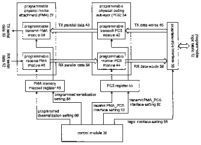
Figure 2 is a schematic block diagram of one
embodiment of a representative one of the programmable
multi-gigabit transceivers 14-28. As shown, the
2~ programmable multi-gigabit transceiver includes a
programmable physical media attachment (PMA) module,32, a
programmable physical coding sub-layer (PCS) module 34, a
programmable interface 36, a control module 35, a PMA
memory mapped register 45 and a PCS register 56. The
3o control module 35, based on the desired mode of operation
for the individual programmable multi-gigabit transceiver
14-28, generates a programmed deserialization setting 66, a
programmed serialization setting 64, a receive PMA PCS
interface setting 62, a transmit PMA PCS interface setting
9

CA 02536624 2006-02-22
WO 2005/027344 PCT/US2004/029864
60, and a logic interface setting 58. The control module
35 may be a separate device within each of the multi-
gigabit transceivers and/or included within the control
module 30. In either embodiment of the PMGT control module
35, the programmable logic device control module 30
determines the corresponding overall desired operating
conditions for the programmable logic device 10 and
provides the corresponding operating parameters for a given
multi-gigabit transceiver to its control module 35, which
so generates the settings 58-66 as will be described in
greater detail with reference to Figures 9 and 10, and
Figures 12A, 12B and 12C.
The programmable physical media attachment (PMA)
module 32 includes a programmable transmit PMA module 38
and a programmable receive PMA module 40. The programmable
transmit PMA module 38, which. will be described in greater
detail in with reference to Figure 6, is operably coupled
to convert transmit parallel data 48 into transmit serial
data 50 in accordance with the programmed serialization
2o setting 64. The programmed serialization setting 64
indicates the desired rate of the transmit serial data 50,
the desired rate of the transmit parallel data 48, and the
data width of the transmit parallel data 48. The
programmable receive PMA module 40, which will be described
in greater detail with reference to Figure 5, is operably
coupled to convert receive serial data 52 into receive
parallel data 54 based on the programmed deserialization
setting 66. The programmed deserialization setting 66
indicates the rate of the receive serial data 52, the
so desired rate of the receive parallel data 54, and the data
width of the receive parallel data 54. The PMA memory
mapped register 45, which will be described in greater
detail with reference to Figure 11, may store the

CA 02536624 2006-02-22
WO 2005/027344 PCT/US2004/029864
serialization setting 64 and the deserialization setting
66.
The programmable physical coding sub-layer (PCS)
module 34 includes a programmable transmit PCS module 42
and a programmable receive PCS module 44. The programmable
transmit PCS module 42, which will be described in greater
detail with reference to Figure 8, receives transmit data
words 46 from the programmable logic fabric 12 via the
programmable interface 36 and converts them into the
io transmit parallel data 48 in accordance with the transmit
PMA PCS interface setting 60. The transmit PMA PCS
interface setting 60 indicates the rate of the transmit
data words 46, the size of the transmit data words (e. g.,
1-byte, 2-bytes, 3-bytes, 4-bytes, et cetera) and the
i5 corresponding transmission rate of the transmit parallel
data 48. The programmable receive PCS module 44, which
will be described in greater detail with reference to
Figure 7, converts the received parallel data 54 into
received data words 56 in accordance with the receive
2o PMA PCS interface setting 62. The received PMA PCS
interface setting 62 indicates the rate at which the
received parallel data 54 will be received, the width of
the parallel data 54, the transmit rate of the received
data words 56 and the word size of the received data words
25 56.
The control module 35 also generates the logic
interface setting 58 that provides the rates at which the
transmit data words 46 and receive data words 56 will be
transceived with the programmable logic fabric 12. Note
3o that the transmit data words 46 may be received from the
programmable logic fabric 12 at a different rate than the
received data words 56 are provided to the programmable
logic fabric 12.
11

CA 02536624 2006-02-22
WO 2005/027344 PCT/US2004/029864
As one of average skill in the art will appreciate,
each of the modules within the PMA module 32 and PCS module
34 may be individually programmed to support a desired data
transfer rate. The data transfer rate may be in accordance
with a particular standard, as those indicated in Figures
12A-12C, such that the receive path, i.e., the programmable
receive PMA. module 40 and the programmable receive PCS
module 44 may be programmed in accordance with one standard
while the transmit path, i.e., the programmable transmit
Zo PCS module 42 and the programmable transmit PMA module 38
may be programmed in accordance with another standard.
Figure 3 illustrates an alternate schematic block
diagram of a representative one of the programmable multi-
gigabit transceivers 14-28. In this embodiment, the
programmable multi-gigabit transceiver 14-28 includes a
transmit section 70, a receive section 72, the control
module 35 and the programmable interface 36. The transmit
section 70 includes the programmable transmit PMA module 38
and the programmable transmit PCS module 42. The receive
2o section 72 includes the programmable receive PMA module 40
and the programmable receive PCS module 44.
In this embodiment, the control module 35 separately
programs the transmit section and the receive section via
transmit setting 74 and receive setting 76, respectively.
The control module 35 also programs the programmable
interface 36 via the logic interface setting 58.
Accordingly, the control module 35 may program the receiver
section 72 to function in accordance with one standard
while programming the transmit section 70 in accordance
3o with another standard. Further, the logic interface
setting 58 may indicate that the transmit data words 46 are
received from the programmable logic fabric 12 at a
different rate than the received data words 56 are provided
to the programmable logic fabric 12. As one of average
12

CA 02536624 2006-02-22
WO 2005/027344 PCT/US2004/029864
skill in the art will appreciate, the programmable
interface 36 may include a transmit buffer and a receive
buffer, and/or an elastic store buffer to facilitate the
providing and receiving of the data words 46 and 56 to-and-
from the programmable logic fabric 12.
Figure 4 is an alternate schematic block diagram of a
programmable logic device 80. The programmable logic
device 80 includes the programmable transmit PMA module 38,
the programmable transmit PCS module 42, the programmable
so interface 36, the programmable logic fabric 12, the
programmable receive PCS module 44, the programmable
receive PMA module 40, and a clock management module 82.
The clock management module 82 receives a plurality of
clock sources 84 and provides one or more of them as a
reference clock 86 to the programmable transmit PMA module
38 and the programmable receive PMA modula 40. The
plurality of clock sources 84 includes, but is not limited
to, a low fitter external clock source, a recovered clock
source as may be produced by the programmable receive PMA
2o module 40, an internal clock of the programmable logic
fabric 12, and/or a system clock. While the clock
management module 82 in Figure 4 is shown to produce a
single reference clock 86 that is provided to both the
programmable transmit PMA module 38 and the programmable
receive PMA module 40, the clock management module 82, in
an alternative embodiment, may generate a separate transmit
reference clock that is provided to the programmable
transmit PMA module 38 and a separate receive reference
clock that would be provided to the programmable receive
3o PMA module 40.
The programmable receive PMA module 40, which will be
described in greater detail with reference to Figure 5,
receives the reference clock 86 and generates therefrom a
serial receive clock 98. In addition, the programmable
13

CA 02536624 2006-02-22
WO 2005/027344 PCT/US2004/029864
receive PN1A module 40 generates a parallel receive clock 94
and a receive programmable logic clock 96 based on the
reference clock 86 and/or the serial receive clock 98. The
programmable receive PMA module 40 receives the serial data
52 and, after being initialized based on the reference
clock 86, recovers the serial receive clock 98 therefrom.
The programmable receive PMA. module 40 converts the receive
serial data 52 into the receive parallel data 54 in
accordance with the serial receive clock 98 and the
so parallel receive clock 94. The programmable receive PMA
module 40 provides the parallel receive clock 94 to the
programmable receive PCS module 44, which converts the
receive parallel data 54 into the receive data words 56 in
accordance with the parallel receive clock 94. The
programmable receive PMA module 40 provides the receive
programmable logic clock 96 to the programmable logic
fabric 12, which processes the receive data words 56 in
accordance with the receive programmable logic clock 96.
Since the serial receive clock, the parallel receive clock,
2o and the receive programmable logic clock are derived from
the same reference clock, the conveyance of data between
the programmable receive PMA module 40, the programmable
receive PCS module 44, and the programmable logic fabric is
synchronized.
~5 The programmable transmit PMA module 38 receives the
reference clock 86 and produces therefrom a serial transmit
clock 92. In addition, the programmable transmit PMA
module 38 generates a transmit programmable logic clock 90
and a parallel transmit clock 88 from the serial transmit
3o clock 92 and/or from the reference clock 86. The
programmable transmit PMA module 38 provides the transmit
programmable logic clock 90 to the programmable logic
fabric 12, which processes data in accordance with the
transmit programmable logic clock 90 to produce the
14

CA 02536624 2006-02-22
WO 2005/027344 PCT/US2004/029864
transmit data words 46. The programmable transmit PMA
module 38 provides the parallel transmit clock 88 to the
programmable transmit PCS module 42, which converts the
transmit data words 46 into the transmit parallel data 48
in accordance with the parallel transmit clock 88. The
programmable transmit PMA module 38 converts the transmit
parallel data 48 into the transmit serial data 50 in
accordance with the serial transmit clock 92 and the
transmit parallel clock 88. The programmable PMA module 38
so further utilizes the serial transmit clock 92 to transmit
the transmit serial data 50. Since the serial transmit
clock, the parallel transmit clock, and the transmit
programmable logic clock are derived from the same
reference clock, the conveyance of data between the
programmable transmit PMA module 38, the programmable
transmit PCS module 42, and the programmable logic fabric
12 is synchronized.
As one of average skill in the art will appreciate,
the programmable transmit PMA. module 38, the programmable
2o transmit PCS module 42, the programmable interface 36, the
programmable receive PCS module 44 and the programmable
receive PNtA module 40 may be programmed as described with
reference to Figures 2 and/or 3.
Figure 5 illustrates a schematic block diagram of the
programmable receive PMA module 40 that includes a
programmable front-end 100, a data and clock recovery
module 102, and a serial-to-parallel module 104. The
programmable front-end 100 includes a receiver termination
circuit 106 and a receiver amplifier 108. The data and
3o clock recovery module 102 includes a data detection circuit
110 and a phase locked loop 112. The phase locked loop 112
includes a phase detection module 114, a loop filter 116, a
voltage controlled oscillator 118, a 1st divider module 120,
and a 2nd divider module 122.

CA 02536624 2006-02-22
WO 2005/027344 PCT/US2004/029864
The programmable front-end 100 is operably coupled to
receive the receive serial data 52 and produce amplified
and equalized receive serial data 124 therefrom. To
achieve this, the receiver termination circuit 106 is
programmed in accordance with a receive termination setting
126 to provide the appropriate termination for the
transmission line between the programmable receiver PMA
module 40 and the source that originally transmitted the
received serial data 52. The receive termination setting
126 may indicate whether the receive serial data 52 is a
single-ended signal, a differential signal, may indicate
the impedance of the termination line, and may indicate the
biasing of the receiver termination circuit 106. The
receiver termination circuit 106 further biases the receive
serial data 52 and provides the bias adjusted signal to the
receiver amplifier 108. The gain and equalization settings
of the receiver amplifier 108 may be adjusted in accordance
with the equalization setting 128 and the amplification
setting 130, respectively. Note that the receiver
2o termination setting 126, the equalization setting 128, and
the amplification setting 130 are part of the program
deserialization setting 66 provided by the control module
35.
The data and clock recovery circuit 102 receives the
amplified and equalized receive serial data 124 via the
phase detection module 114 of phase locked loop 112 and via
the data detection circuit 110. The phase detection module
114 has been initialized prior to receiving the amplified
and equalized receive serial data 124 by comparing the
3o phase and/or frequency of the reference clock 86 with a
feedback reference clock produced by divider module 120.
Based on this phase and/or frequency difference, the phase
detection module 114 produces a corresponding current that
is provided to loop filter 116. The loop filter 116
16

CA 02536624 2006-02-22
WO 2005/027344 PCT/US2004/029864
converts the current into a control voltage that adjusts
the output frequency of the voltage controlled oscillator
118. The divider module 120, based on a serial received
clock setting 132 or settings within the bit stream,
divides the output oscillation produced by the VCO 118 to
produce the feedback signal. Once the amplified and
equalized receive serial data is received, the phase
detection module 114 compares the phase of the amplified
and equalized receive serial data 124 with the phase of the
Zo amplified and equalized receive serial data 124. Based on
a phase difference between the amplified and equalized
receive serial data 124 and the feedback signal, a current
signal is produced.
The phase detection module 114 provides the current
signal to the loop filter 116, which converts it into a
control voltage that controls the output frequency of the
voltage controlled oscillator 118. At this point, the
output of the voltage controlled oscillator 118 corresponds
to a recovered clock 138. The recovered clock 138, which
ao was referenced as the serial receive clock 98 in Figure 4,
is provided to the divider module 122, the data detection
circuit 110 and to the serial-to-parallel module 104. The
data detection module 110 utilizes the recovered clock 138
to recover data 136 from the amplified equalized receive
serial data 124. The divider module 122 divides the
recovered clock 138, in accordance with a parallel receive
and programmable logic clock setting 134, to produce the
parallel receive clock 94 and the programmable logic
receive clock 96. Note that the serial receive clock
3o setting 132 and the parallel receive and programmable logic
clock setting 134 are part of the programmable
deserialization setting 66 provided to the programmable
receive PMA module 40 by the control module 35.
17

CA 02536624 2006-02-22
WO 2005/027344 PCT/US2004/029864
The serial-to-parallel module 104, which may include
an elastic store buffer, receives the recovered data 136 at
a serial rate in accordance with the recovered clock 138.
Based on a serial-to-parallel setting 135 and the parallel
s receive clock 194, the serial-to-parallel module 104
outputs the receive parallel data 54. The serial-to-
parallel setting 135, which may be part of the programmable
deserialization setting 66, indicates the rate and data
width of the receive parallel data 54.
so Figure 6 illustrates a schematic block diagram of a
programmable transmit PMA module 38 that includes a phase
locked loop 144, a parallel-to-serial module 140, and line
driver 142. The phase locked loop 144 includes a phase
detection module 146, a loop filter 148, a voltage control
s5 oscillator 150, a divider module 154, and a divider module
152.
The phase detection module 146 compares the phase
and/or frequency of the reference clock 86 with the phase
and/or frequency of a feedback oscillation produced by
2o divider module 154. The phase detection module 146
generates a current signal to represent the phase and/or
frequency difference between the reference clock 86 and the
feedback oscillation. The loop filter 148 converts the
current signal into a control voltage that regulates the
25 output oscillation produced by the voltage control
oscillator 150. Divider module 154, based on a serial
transmit clock setting 158, divides the output oscillation
of the VCO 150, which corresponds to the serial transmit
clock 92, to produce the feedback oscillation. Note that
so the serial transmit clock setting 158 may be part of the
programmed serialization setting 64 provided to the
programmable transmit PMA module 38 by the control module
35. Divider module 152 receives the serial transmit clock
92 and, based on a parallel transmit and programmable logic
18

CA 02536624 2006-02-22
WO 2005/027344 PCT/US2004/029864
clock setting 160, produces the parallel transmit clock 88
and the transmit programmable logic clock 90. The parallel
transmit and programmable logic clock setting 160 may be
part of the programmed serialization setting 64.
The parallel-to-serial module 140 receives the
transmit parallel data 48 and produces therefrom a serial
data stream 156. To facilitate the parallel-to-serial
conversion, the parallel-to-serial module 140, which may,
include an elastic stored buffer, receives a parallel-to-
so serial setting 161 to indicate the width of the transmit
parallel data 48 and the rate of the transmit parallel
data, which corresponds to the parallel transmit clock 88.
Based on setting 161, the serial transmit clock 92 and the
parallel transmit clock 88, the parallel-to-serial module
140 produces the serial data stream 156 from the transmit
parallel data 48.
The line driver 142 increases the power of the serial
transmit data 156 to produce the transmit serial data 50.
The line driver 142 may be programmed to adjust its pre-
2o emphasis settings, slew rate settings, and drive settings
via a pre-emphasis setting signal 162, a slew rate setting
signal 164 and a drive setting signal 166. The pre-
emphasis setting 162, slew rate setting 164 and drive
setting 166 may be part of the programmed serialization
2~ setting 64. As one of average skill in the art will
appreciate, while the diagram of Figure 6 is shown as a
single-ended system, the entire system may be differential
signaling and/or a combination of differential and single-
ended signaling.
3o Figure 7 is a schematic block diagram of a
programmable receive PCS module 44 that includes a
programmable data alignment module 170, a programmable
descramble and decode module 172, a programmable storage
module 174, and a programmable decode and verify module
19

CA 02536624 2006-02-22
WO 2005/027344 PCT/US2004/029864
176. The programmable data alignment module 170 includes a
synchronous state machine 178, a value detect realign
module 180, a block synchronization module 182, and a
multiplexer 184. The programmable descramble and decode
module 172 includes a 64b/66b descrambling module 188, an
8b/10b decoding module 186 and a multiplexer 190. The
programmable storage module 174 includes a channel bonding
module 194, an elastic storage buffer 192 and a multiplexer
196. The programmable decode and verify module 176
io includes a receiver CRC (cycle redundancy check) module
200, a 64b/66b decoding module 198, and a multiplexer 202.
In operation, the programmable data alignment module
170 receives the receive parallel data 54. Based on the
receive PMA PCS interface setting 62, the receive parallel
data 54 may be passed via multiplexer 184 without
processing, may be processed by the value detect realign
module 180 and then passed via multiplexer 184 and/or
further processed via the block synchronization module 182.
As such, the setting 62 may bypass the programmable data
2o align module 170, perform a value detection realignment and
pass the realigned data and/or further utilize block
synchronization, which is typically used for 10 gigabits-
per-second signaling. The synchronization state machine
178 coordinates the alignment of the receive parallel data
54 via the value detect realign 180 and the block
synchronization module 182. In addition, once the value
detect realignment module 180 indicates that the data is
valid and the block synchronization module 182 indicates
that the PCS module is now in sync with the receive
so parallel data 54, the sync state machine 178 generates a
lock signal.
The controls of the value detect realign module 180
include receiver polarity of the signal, alignment
information, et cetera.

CA 02536624 2006-02-22
WO 2005/027344 PCT/US2004/029864
The programmable descramble and decode module 172
receives the output of multiplexes 184 and, based on
setting 62, either passes the data via multiplexes 190
descrambles it via the 64b/66b descrambler 188 or decodes
it via the 8b/10b decode module 186.
The programmable storage module 174 may buffer the
data it receives from multiplexes 190 via the elastic store
buffer 192 to facilitate channel bonding or pass the data
directly to multiplexes 196. The channel bonding module
Zo 194 enables the receiver of one programmable multi-gigabit
transceiver to be linked or bonded with another receiver
within another multi-gigabit transceiver to increase the
effective serial data rate.
The programmable decode and verify module 176 receives
the output of multiplexes 196 and passes it directly as the
receive data word 56 in accordance with setting 62,
processes the data via a receive CRC module 200 and
provides that as the output, or decodes it via the 64b/66b
decoding module 198. As one of average skill in the art
2o will appreciate, the programmable receive PCS module 44 is
readily programmable via settings 62 to decode the received
parallel data 54 using ~a variety of decoding schemes, to
process channel bonding, to verify and lock the incoming
data, et cetera.
Figure 8 is a schematic block diagram of the
programmable transmit PCS module 42 that includes a
programmable verify module 210, a programmable encode
module 212, a programmable storage module 214, and a
programmable scramble module 216. The programmable verify
3o module 210 includes a transmit CRC module 218 and a
multiplexes 220. The programmable encode module 212
includes a 64b/66b encoding module 222, an 8b/10b encoding
module 224, and a multiplexes 226. The programmable
storage module 214 includes an elastic storage buffer 228
21

CA 02536624 2006-02-22
WO 2005/027344 PCT/US2004/029864
and a multiplexer 230. The programmable scramble module
216 includes a scramble module 232, a gearbox module 234,
and a PMA converter'236.
The programmable verify module 210 is operably coupled
to receive the transmit data words 46 and either pass them
directly to the programmable encoding module 212 or perform
a cycle redundancy check upon them. The transmit PMA PCS
interface setting 60 indicates whether the transmit data
words 46 will be directly passed to the programmable encode
Zo module 212 or be subject to a cycle redundancy check. The
programmable encoding module 212, based on setting 60,
either encodes the data received from the programmable
verify module 210 via the 8b/10b encoder 224, the 64b/66b
encoder 222 or passes the data directly to the programmable
storage module 214.
The programmable storage module 214, based on setting
60, either passes the data that it receives from the
programmable encode module 212 or stores it in the elastic
storage buffer 228. The elastic storage buffer 228 allows
2o for differing,time rates between the transmit data words 46
and the transmit parallel data 48. For example, if the
transmit data words 46 are 1-byte words at a rate of 500
megahertz and the transmit parallel data 48 is 2-bytes
width at 300 megahertz, the data-per-cycle rate is
different between the transmit data words 46 and the
transmit parallel data 48. Accordingly, the elastic
storage buffer 228 allows for data to accumulate in the
elastic storage buffer and thus accommodate the differing
data-per-rate discrepancies between the transmit data word
so 46 and the transmit parallel data 48.
The programmable scramble module 216 receives the
output of multiplexer 230 and either passes it directly to
the PMA converter 236 to produce the transmit parallel data
48 based on control signals or scrambles the data via the
22

CA 02536624 2006-02-22
WO 2005/027344 PCT/US2004/029864
scramble module 232 and the gearb~x module 234. The
controls for the PMA converter 236 include polarity of the
parallel data 48 and an indication of which path the data
will be received from. The scramble module 232 and gearbox
module 234 are further described in co-pending patent
application by Joseph N. Kryzak et al. entitled FRAMING OF
TRANSMIT ENCODED DATA AND LINEAR FEEDBACK SHIFTING and
having the same filing date as the present application.
As one of average skill in the art will appreciate,
Zo the programmable transmit PCS module 42 may be programmed
in a variety of ways to directly pass the transmit data
words 46, encode them, scramble them, buffer them, et
cetera. As such, with a wide diversity in programming
abilities, the programmable transmit PCS module 42 as well
25 as the entire programmable multi-gigabit transceiver may be
programmed in accordance with many standards.
Figure 9 illustrates a logic diagram of a method for
establishing the settings for the programmable multi-
gigabit transceivers. Such a method may be performed by
2o the control module 30 and/or control module 35. The
process begins at Step 240 where a programming setting that
indicates the desired mode-of-operation for the
programmable multi-gigabit transceiver (PMGT) is received.
The primitive may be received based on a user selection
25 and/or based on an auto configuration process. Such an
auto configuration process would sense the environment in
which the PMGT is located to determine its operating mode.
A primitive, which will be described in greater detail in
Figures 12A-12C, generally indicates a particular
so application of a corresponding standard. For example, with
reference to Figure 12A, the primitive GT10-10GFC_8
corresponds to the 10-gig fiber-channel standard that
provides a serial transmission rate of 10.51875 gigabits-
23

CA 02536624 2006-02-22
WO 2005/027344 PCT/US2004/029864
per-second, utilizes 64b/66b encoding and has a fabric
interface of 64-bits data words at 159.37 megahertz.
Returning to the discussion of Figure 9, the process
continues at Step 242 where the programming setting is
converted into the programmed serialization setting, the
programmed deserialization setting, the receive PMA PCS
interface setting, the transmit PMA PCS interface setting
and the logic interface setting. As previously mentioned,
the primitive indicates the particular application of a
Zo standard. As such, the primitive will indicate the serial
transmission rate, the corresponding encoding and the
fabric interface rate. Accordingly, based on these values,
the settings, which program the PMGT are established.
The process then proceeds to Step 244 where the ,
programmed serialization setting and the programmed
deserialization setting are provided to the PMA memory
mapped register. The PMA memory mapped register will be
further described with reference to Figure 11. The process
then proceeds to Step 246 where the transmit and receive
2o PMA PCS interface settings and the programmable logic
interface settings are provided to the PCS register. Once
the settings are stored in the appropriate registers, the
PMA sections of the PMGT and the PCS sections of the PMGT
are correspondingly programmed as described in Figures 5-8.
Figure 10 is a logic diagram of a method that further
indicates the programming of the programmable MGT by
control module 30 and/or control module 35. The process
begins at Step 250 where the programmed serialization
setting is generated to enable, logically disable and/or
3o physically disable at least one element of the programmable
PMA receiver module. For example, with reference to Figure
5, the programmed serialization setting 66 may be used to
enable and/or disable the programmable front-end 100, the
phase locked loop 112, the data detection circuit 110
24

CA 02536624 2006-02-22
WO 2005/027344 PCT/US2004/029864
and/or the serial-to-parallel module 104. The elements to
be disabled are based on the particular mode-of-operation.
If data is not being received, the entire programmable
received PMA module may be disabled thus conserving power.
Returning to the discussion of Figure 10, the process
proceeds to Step 252 where the programmed deserialization
setting is generated to enable, logically disable or
physically disable at least one element of the programmable
PMA transmitter module. For example, with reference to
so Figure 6, the programmed serialization setting 64 may
enable or disable physically (i.e., remove power there
from) or logically disable (i.e., logically hold an input
or output to a known state) the phase locked loop 144, the
parallel-to-serial module 140, and/or the line-driver 142.
Returning to the discussion of Figure 10, the process
then proceeds to Step 254 where the transmit PMA PCS
interface setting is generated to enable, logically disable
and/or physically disable at least one element of the
programmable PCS transmit module. The process then
2o proceeds to Step 256 where the received PMA PCS interface
setting is generated to enable, logically disable and/or
physically disable at least one element of the programmable
PCS received module. The elements of the programmable PCS
transmit module are shown in Figure 8 and the elements of
the programmable receive PCS module are shown in Figure 7.
Figure 11 illustrates the contents of the PMA mapping
register 45. As shown, the mapping register includes
memory spaces for indicating a variety of operations for
the PMA. module including a master bias, transmit divider
3o ratio, transmit loop filter settings, transmit mode
control, transmit output level, transmit output mode,
receive divider ratio, receive loop filter settings,
received mode of operation, received forward error encoding
and power control of the PMA module.

CA 02536624 2006-02-22
WO 2005/027344 PCT/US2004/029864
Figures 12A-12C illustrate a plurality of primitives, their
corresponding standards, serial rate, encoding scheme and
fabric interface rate. Accordingly, any of these
primitives, or programming settings, may be selected by a
user of the device and the corresponding settings derived
to program the programmable logic device to support the
particular standard.
The preceding discussion has presented a programmable
logic device that includes programmable multi-gigabit
1o transceivers. The mufti-gigabit transceivers have
separately programmable transmit paths and receive paths
and may be independently programmed from one another within
the programmable logic device. As such, a great deal of
flexibility is provided via such a programmable logic
device. As one of average skill in the art will
appreciate, other embodiments may be derived from the
teaching of the present invention without deviating from
the scope of the claims.
26

Representative Drawing
A single figure which represents the drawing illustrating the invention.
Administrative Status

2024-08-01:As part of the Next Generation Patents (NGP) transition, the Canadian Patents Database (CPD) now contains a more detailed Event History, which replicates the Event Log of our new back-office solution.

Please note that "Inactive:" events refers to events no longer in use in our new back-office solution.

For a clearer understanding of the status of the application/patent presented on this page, the site Disclaimer , as well as the definitions for Patent , Event History , Maintenance Fee  and Payment History  should be consulted.

Event History

Description Date
Inactive: Associate patent agent added 2022-02-22
Inactive: IPC expired 2022-01-01
Revocation of Agent Requirements Determined Compliant 2021-12-31
Appointment of Agent Requirements Determined Compliant 2021-12-31
Inactive: IPC from PCS 2021-12-04
Inactive: First IPC from PCS 2021-12-04
Inactive: IPC assigned 2020-05-23
Inactive: IPC assigned 2020-05-22
Inactive: IPC expired 2020-01-01
Inactive: IPC removed 2019-12-31
Common Representative Appointed 2019-10-30
Change of Address or Method of Correspondence Request Received 2019-02-19
Inactive: IPC expired 2015-01-01
Inactive: IPC removed 2014-12-31
Grant by Issuance 2009-06-02
Inactive: Cover page published 2009-06-01
Inactive: Final fee received 2009-03-05
Pre-grant 2009-03-05
Amendment After Allowance (AAA) Received 2009-02-25
Notice of Allowance is Issued 2009-01-09
Letter Sent 2009-01-09
Amendment After Allowance (AAA) Received 2009-01-09
Inactive: IPC assigned 2008-12-22
Inactive: First IPC assigned 2008-12-22
Inactive: IPC assigned 2008-12-22
Inactive: First IPC assigned 2008-11-24
Inactive: IPC removed 2008-11-24
Inactive: IPC assigned 2008-11-24
Inactive: Approved for allowance (AFA) 2008-11-19
Letter Sent 2008-11-14
Advanced Examination Requested - PPH 2008-11-04
Request for Examination Requirements Determined Compliant 2008-11-04
All Requirements for Examination Determined Compliant 2008-11-04
Amendment Received - Voluntary Amendment 2008-11-04
Request for Examination Received 2008-11-04
Advanced Examination Determined Compliant - PPH 2008-11-04
Inactive: Cover page published 2006-04-28
Inactive: Notice - National entry - No RFE 2006-04-25
Letter Sent 2006-04-25
Application Received - PCT 2006-03-15
Amendment Received - Voluntary Amendment 2006-02-22
National Entry Requirements Determined Compliant 2006-02-22
Application Published (Open to Public Inspection) 2005-03-24

Abandonment History

There is no abandonment history.

Maintenance Fee

The last payment was received on 2008-07-21

Note : If the full payment has not been received on or before the date indicated, a further fee may be required which may be one of the following

  • the reinstatement fee;
  • the late payment fee; or
  • additional fee to reverse deemed expiry.

Patent fees are adjusted on the 1st of January every year. The amounts above are the current amounts if received by December 31 of the current year.
Please refer to the CIPO Patent Fees web page to see all current fee amounts.

Owners on Record

Note: Records showing the ownership history in alphabetical order.

Current Owners on Record
XILINX, INC.
Past Owners on Record
AARON J. HOELSCHER
ANDREW G. JENKINS
CHARLES W. BOECKER
ERIC D. GROEN
JOSEPH N. KRYZAK
SCOTT A. IRWIN
WILLIAM C. BLACK
YIQIN CHEN
Past Owners that do not appear in the "Owners on Record" listing will appear in other documentation within the application.
Documents

To view selected files, please enter reCAPTCHA code :


To view images, click a link in the Document Description column. To download the documents, select one or more checkboxes in the first column and then click the "Download Selected in PDF format (Zip Archive)" or the "Download Selected as Single PDF" button.

List of published and non-published patent-specific documents on the CPD .

If you have any difficulty accessing content, you can call the Client Service Centre at 1-866-997-1936 or send them an e-mail at CIPO Client Service Centre.


Document
Description 
Date
(yyyy-mm-dd) 
Number of pages   Size of Image (KB) 
Description 2006-02-21 26 1,364
Claims 2006-02-21 9 404
Drawings 2006-02-21 13 614
Abstract 2006-02-21 2 78
Representative drawing 2006-02-21 1 24
Claims 2008-11-03 31 1,109
Claims 2006-02-22 6 258
Representative drawing 2008-11-19 1 14
Reminder of maintenance fee due 2006-05-10 1 112
Notice of National Entry 2006-04-24 1 206
Courtesy - Certificate of registration (related document(s)) 2006-04-24 1 129
Acknowledgement of Request for Examination 2008-11-13 1 190
Commissioner's Notice - Application Found Allowable 2009-01-08 1 163
PCT 2006-02-21 5 175
Fees 2006-07-17 1 30
Fees 2007-07-22 1 32
Fees 2008-07-20 1 32
Correspondence 2009-03-04 1 37
Fees 2009-08-24 1 35
Prosecution correspondence 2009-01-08 1 40