Note: Descriptions are shown in the official language in which they were submitted.
CA 02537825 2013-01-23
ELECTRICAL WIRE AND METHOD
OF FABRICATING THE ELECTRICAL WIRE
BACKGROUND OF THE INVENTION
Field of the Invention
The present invention generally relates to an electrical wire and method of
fabricating the wire, and more particularly, an electrical wire which includes
at least one
Electrifiable conductor (e.g., having a purpose of carrying an electrical
current, e.g., an
alternating current (AC) or direct current (DC) power supply, or a
communication signal
such as a voice or data transmission signal), and a return conductor (e.g.,
first and second
return conductors) which at least substantially entraps the Electrifiable
conductor.
Description of the Related Art
The earliest forms of wiring homes (1920s -1950s) utilized wire insulated with
shellac permeated cloth wrap. Asphalted cloth wrap was used for insulation in
the 1950s-
1970s. Aluminum electrical wiring was installed in homes in the mid 1960s
through the
mid 1970s. Wire, as we know it today with two insulated inner conductors
(e.g.,
hot/neutral or
1
CA 02537825 2006-03-03
WO 2005/024849 PCT/US2004/028972
Electrifiable/return conductors) and a non-insulated ground conductor (e.g.,
grounding
conductor), all within a thermoplastic outer insulator, has been used since
the mid-1950s.
Figures 1A-1B illustrate examples of such conventional electrical wire. As
illustrated in
Figure 1A, one conventional electrical wire 50 includes an Electrifiable
(e.g., hot) conductor 55
surrounded by a first insulation layer 60, a return (e.g., neutral) conductor
65 surrounded by a
second insulation layer 70. A third insulation layer 75 surrounds the
insulated conductors 55, 65.
As illustrated in Figure 1B, another conventional electrical wire 100 includes
an
Electrifiable (e.g., hot) conductor 105 surrounded by a first insulation layer
110, a return
conductor 115 surrounded by a second insulation layer 120, and a grounding
conductor 125. A
third insulation layer 130 surrounds all of the conductors 105, 115 and 125.
Many millions of homes today are facing end-of-life scenarios regarding their
older
wiring and run significant risk of fire damage and casualties. According to
the National Science
and Technology Council November 2000 report, "[w]ire systems may become
unreliable or fail
altogether, due to poor design, use of defective materials, improper
installation, or other causes.
The risk of failure increases as wire systems age, due to cumulative effects
of environmental
stresses (e.g. heat, cold, moisture, or vibration), inadvertent damage during
maintenance, and the
wear and tear of constant use. The aging of a wire system can result in loss
of critical function in
equipment powered by the system... can jeopardize public health and safety and
lead to
catastrophic equipment failure or to smoke and fire." The Consumer Products
Safety
Commission estimates that 50 million homes in the United States have reached
or are about to
reach the "end-of-life" of their electrical wiring system.
Furthermore, wire insulation and/or conductors can deteriorate due to
radiation, high
2
CA 02537825 2006-03-03
WO 2005/024849 PCT/US2004/028972
temperature, steam, chafing, mishandling, corrosion, mechanical loading, and
vibration. Reports
issued by the Consumer Products Safety Commission (CPSC) show that in 1997
home wire
systems caused over 40,000 fires that resulted in 250 deaths and over $670
million of property
damage. Further study by the CPSC based on 40,300 electrical circuit fires
showed that 36%
were due to installed wiring and 16% were due to cord/plugs. Along with the
usual wire system
failures due to age and environmental stresses, aluminum wire systems were
"prone to
degradation and dangerous overheating".
Regarding modern wire systems and technology, the National Institute of
Standards and
Technology (NIST) and Building and Fire Research Laboratory (BFRL)
acknowledge, "[w]ires
and cables made with fluorocarbons have excellent flammability, but are very
expensive. Flame-
retarded polyvinyl chloride (PVC) cables also have excellent flammability and
physical
properties... However, the chloride content of (all) PVC cables is a concern
for potential
formation of dioxin during incineration."
As illustrated in Figures 1A-1B, conventional electrical wire which is
commonly used in
homes and offices today consist of solid, round wires individually insulated
with PVC (except for
the ground wire) with an outer PVC jacket surrounding the inner wires. Fires
are increasingly
being caused by overheated wires, insulation breakdown, and penetrations. The
open spaces
afforded by conventional in-wall or in-ceiling wiring offer plenty of oxygen
for fire ignition and
expansion associated with electrical fires.
Moreover, such conventional electrical wire poses an electric shock hazard and
therefore,
causes safety concerns. That is, such conventional electrical wire is often
accidentally penetrated
by objects such as nails, screws, drill bits, etc. which often results in the
serious injury or death.
3
CA 02537825 2006-03-03
WO 2005/024849 PCT/US2004/028972
Thus, such conventional electrical wire has a high potential for serious
injury when penetrated by
any of the aforementioned electrically conductive objects.
Other key examples of conventional wiring systems being inadequate in the
changing-
marketplace include:
(a) the proliferation of solid wall (and ceiling) construction techniques;
and
(b) the proliferation of new technologies and devices being
installed in new and
especially existing home and office environments that require wire interfaces
and many are
designed for surface mounting of these devices.
New materials such as foam block forms for poured concrete walls, removable
form
poured concrete walls, fabricated alternative materials to wood and recycled
materials formed
into solid wall (and ceiling) panels all represent better long-term
characteristics and advantages
over current "hollow" exterior and interior wall (and ceiling)construction
techniques. These
solid material construction techniques require some type of invasive
channeling done on-site.
This channeling has many drawbacks, safety concerns and costs associated. It
also typically
places the wiring closer to the finished surface where future invasions as
previously described
may cause shock or potential arch faults and fire potential. On a global scale
the construction
issues have existed for many years based on differences in construction
techniques.
In addition, the advent of advances in audio, video and computer/internet
applications
have drastically changed the paradigm of home and office devices. Surround-
sound home theater
and multi-media conference room audio systems, flat-panel plasma and liquid
crystal display
(LCD) televisions, networked homes and offices, new applications of lighting,
air quality and
control systems have put tremendous strains and in many cases compromises on
wiring systems.
4
CA 02537825 2006-03-03
WO 2005/024849 PCT/US2004/028972
The requirement for alternating current (AC) or direct current (DC) electrical
power interfaces
and the associated wiring has created problems for the installer and the user.
SUMMARY OF THE INVENTION
In view of the foregoing, and other problems, disadvantages, and drawbacks of
conventional methods, an exemplary aspect of the embodiments of the present
invention
provides an electrical wire and method of fabricating the electrical which may
provide a safe and
convenient electrical wire which is easily fabricated.
The inventors have determined that a new wiring system that is inherently safe
and is
The exemplary aspects of the present invention include an electrical wire
which includes
at least one electrifiable conductor, and first and second return conductors
(e.g., at least one
20 Further, the electrical wire may be surface-mountable and may be safely
used for
practically any voltage application (e.g., OV to 240V or higher).
The wire may further include first and second insulating layers which are
formed
5
CA 02537825 2006-03-03
WO 2005/024849 PCT/US2004/028972
between the at least one electrifiable conductor and the first and second
return conductors,
respectively. Further, the at least one electrifiable conductor and the first
and second return
conductors may include substantially flat conductive layers having a stacked
arrangement. The
wire may also include an outer insulating layer (e.g., third and fourth
insulating layers) formed on ,
the first and second return conductors.
In addition, a distance between the at least one electrifiable conductor and
each of the first
and second return conductors (e.g., a thickness of an insulating layer between
these conductors)
is no greater than about 0.030 inches. For example, in one exemplary
embodiment, this distance
is no more than about 0.005 inches. Further, the first and second return
conductors may contact
each other along a longitudinal edge (e.g., at the edge of the width) of the
electrical wire, such
that the electrifiable conductor is completely entrapped (e.g., completely
surrounded) by the first
and second return conductors.
In addition, additional protection may be provided by working (e.g., treating)
the
longitudinal edges of the insulating layers, return conductors and/or
grounding conductors. For
example, the first and second return conductors may be treated by at least one
method of
mechanical, thermal or chemical treatment to form a protective longitudinal
edge of the electrical
wire, the protective edge inhibiting a foreign object from penetrating the
electrical wire and
contacting the Electrifiable conductor without contacting one of the first and
second return
conductors.
Similarly, the first and second insulating layers may contact each other along
a
longitudinal edge of the electrical wire. Further, the first and second
insulating layers may be
treated by at least one method of mechanical, thermal or chemical treatment to
form a protective
6
CA 02537825 2006-03-03
WO 2005/024849 PCT/US2004/028972
longitudinal edge of the electrical wire, the protective edge inhibiting a
foreign object from
penetrating the electrical wire and contacting the Electrifiable conductor.
Another aspect of the present invention includes an electrical wire including
at least one
electrifiable conductor, first and second insulating layers formed on opposing
sides of the at least
one electrifiable conductor, first and second return conductors formed on the
first and second
insulating layers, respectively, such that the at least one electrifiable
conductor is at least
substantially entrapped by the first and second return conductors, third and
fourth insulating
layers formed on the first and second return conductors, respectively, first
and second grounding
conductors formed on the third and fourth insulating layers, respectively, and
fifth and sixth
insulating layers formed on the first and second grounding conductors,
respectively.
Further, the at least one Electrifiable conductor may include a plurality of
Electrifiable
conductors, formed in a plurality of horizontal segments across a width of the
wire and a plurality
of vertical segments across a thickness of the wire. In addition, at least one
segment in the
plurality of horizontal segments of the Electrifiable conductors may be used
to transmit a
communication signal (e.g., a voice communication signal and/or a data
communication signal)
and at least one segment in the plurality of horizontal segments of the
Electrifiable conductors
may be used to supply AC or DC electrical power.
Further, a capacitance formed between the at least one Electrifiable conductor
and the
first and second return conductors may be given as C = 1.5 =W =L =s/d, where W
is the width of
the return and electrifiable conductors, L is the length of the return and
electrifiable conductors, s
is the dielectric constant for the insulating layers (e.g., dielectric between
the return and
7
CA 02537825 2006-03-03
WO 2005/024849 PCT/US2004/028972
eleetrifiable conductors, and d is the distance between each of the return and
electrifiable
conductors.
In addition, the first and second grounding conductors may inhibit power
transmission
signals and load-generated electrical noise from being generated in the
electrical wire. Further,
the first and second return conductors and the first and second grounding
conductors may be
(e.g., substantially) thermally conductive for dissipating heat from the at
least one Electrifiable
conductor. Specifically, the first and second return conductors and the first
and second grounding
conductors may have (e.g., each may have) a rate of heat dissipation which is
greater than a rate
of heat dissipation for a round conductor, for a given cross-sectional area.
An important advantage of an exemplary embodiment of the present invention, is
that
substantially flat conductors may have a larger surface area than a round
conductor (e.g., for a
given conductor cross-sectional area). The increased surface area provides a
much greater heat
transfer rate. Since the cross-sectional geometry may not substantially vary
with respect to
longitudinal direction, the pertinent variable is the perimeter along the edge
of any given
conductor and how it varies when the total cross-sectional area is maintained
constant.
The substantially flat conductors can, therefore, carry a greater amount of
electricity for a
given cross-sectional area (e.g., of the conductor) if the resulting steady-
state temperature is kept
constant and if surrounding environment is kept constant. Alternatively, the
steady-state
temperature would be lower on substantially fiat conductors (versus round
conductors) if the
current flow is maintained constant and all other factors remain the same
Further, it may be preferable for the wire to have a thickness ratio of about
1 or more.
That is, the first and second return conductors may each have a thickness TG,
and the first and
8
CA 02537825 2006-03-03
WO 2005/024849 PCT/US2004/028972
second grounding conductors each have a thickness TN, and the Electrifiable
conductor has a
thickness TH, such that a ratio, R, of thicknesses R = (TG + TN)/TH is about
1.00 or more (e.g., it
may be preferable that R is maximized).
Another aspect of the present invention includes an electrical wire including
at least one
electrifiable conductor, a first insulating layer formed around the at least
one electrifiable
conductor, a return conductor formed around (e.g., at least substantially
around) the first
insulating layer, such that the at least one electrifiable conductor is at
least substantially
entrapped by the return conductor, and a second insulating layer formed around
the return
conductor. The wire may further include a grounding conductor formed around
the second
insulating layer, and a third insulating layer formed around the grounding
conductor.
This aspect of the wire may include, for example, a wire having conductors
(e.g.,
electrifiable conductor, return conductor and grounding conductor) having one
of substantially
curvilinear-shaped cross-sectional geometries and substantially rectilinear
cross-sectional
geometries, and may be formed in substantially parallel planes. For example,
the electrical wire
may have a circular or oval cross-section. That is, the electrifiable
conductor, the return
conductor and the grounding conductor may include substantially circular-
shaped conductors
(e.g., having a circular cross-section) which are arranged with a parallel
longitudinal axes (e.g.,
coaxial), or the electrifiable conductor, the return conductor and the
grounding conductor may
include substantially oval-shaped conductors (e.g., in the same spatial
arrangement).
Another aspect of the present invention includes a method of fabricating an
electrical
wire, which includes forming at least one electrifiable conductor, and forming
first and second
return conductors on opposing sides of the at least one electrifiable
conductor, such that the at
9
CA 02537825 2009-10-01
,
least one electrifiable conductor is at least substantially entrapped by the
return
conductors.
Another aspect of the present invention includes an electrical current
delivery
system including the electrical wire. In addition, another aspect of the
present invention is
an electrical signal transmission system including the electrical wire.
In another aspect of the invention, there is provided an electrical wire
comprising
at least one electrifiable conductor for delivering electrical power; a return
conductor
formed around said at least one electrifiable conductor, such that said at
least one
electrifiable conductor is completely entrapped by said return conductor a
first insulating
layer formed between said at least one electrifiable conductor and said return
conductor;
and a second insulating layer formed around said return conductor.
In another aspect of the invention, there is provided an electrical wire
comprising
at least one electrifiable conductor for delivering electrical power; a return
conductor
formed around said at least one electrifiable conductor, such that said at
least one
electrifiable conductor is completely entrapped by said return conductor; a
first insulating
layer formed between said at least one electrifiable conductor and said return
conductor; a
grounding conductor formed around said return conductor; a second insulating
layer
formed between said return conductor and said grounding conductor; and a third
insulating
layer formed on said grounding conductor.
In yet another aspect of the invention, there is provided an electrical wire
comprising at least one electrifiable conductor for delivering electrical
power; and first
and second return conductors which are respectively formed on opposing sides
of said at
least one electrifiable conductor, such that said at least one electrifiable
conductor is at
CA 02537825 2009-10-01
least substantially entrapped by said first and second return conductors;
wherein a distance
between said at least one electrifiable conductor and each of said first and
second return
conductors is no greater than approximately 0.030 inches.
In yet another aspect of the invention, there is provided an electrical wire
comprising at least one electrifiable conductor for delivering electrical
power; first and
second insulating layers formed on opposing sides of said at least one
electrifiable
conductor; first and second return conductors formed on said first and second
insulating
layers, respectively, such that said at least one electrifiable conductor is
at least
substantially entrapped by said first and second return conductors; third and
fourth
insulating layers formed on said first and second return conductors,
respectively; first and
second grounding conductors formed on said third and fourth insulating layers,
respectively; and fifth and sixth insulating layers formed on said first and
second
grounding conductors, respectively; wherein a distance between said at least
one
electrifiable conductor and each of said first and second return conductors is
no greater
than approximately 0.030 inches.
In yet another aspect of the invention, there is provided an electrical wire
comprising at least one electrifiable conductor for delivering electrical
power; a first
insulating layer formed around said at least one electrifiable conductor; a
return conductor
formed around said first insulating layer, such that said at least one
electrifiable conductor
is at least substantially entrapped by said return conductor; and a second
insulating layer
formed around said return conductor;
wherein a distance between said at least one electrifiable conductor and said
return
conductor is no greater than approximately 0.030 inches.
10a
CA 02537825 2009-10-01
In yet another aspect of the invention, there is provided a method of
fabricating an
electrical wire, comprising forming at least one electrifiable conductor for
delivering
electrical power; and forming first and second return conductors on opposing
sides of said
at least one electrifiable conductor, such that said at least one
electrifiable conductor is at
least substantially entrapped by said return conductors; wherein a distance
between said at
least one electrifiable conductor and each of said first and second return
conductors is no
greater than approximately 0.030 inches.
In yet another aspect, there is provided an electrical wire comprising at
least one
electrifiable conductor for delivering electrical power; and first and second
return
conductors which are respectively formed on opposing sides of said at least
one
electrifiable conductor, such that said at least one electrifiable conductor
is at least
substantially entrapped by said first and second return conductors; wherein a
total
thickness of the electrical wire is no more than approximately 0.050 inches.
In yet another aspect, there is provided an electrical wire comprising at
least one
electrifiable conductor for delivering electrical power; first and second
insulating layers
formed on opposing sides of said at least one electrifiable conductor; first
and second
return conductors formed on said first and second insulating layers,
respectively, such that
said at least one electrifiable conductor is at least substantially entrapped
by said first and
second return conductors; third and fourth insulating layers formed on said
first and
second return conductors, respectively; first and second grounding conductors
formed on
said third and fourth insulating layers, respectively; and fifth and sixth
insulating layers
formed on said first and second grounding conductors, respectively; wherein a
total
thickness of the electrical wire is no more than approximately 0.050 inches.
10b
CA 02537825 2009-10-01
In yet another aspect, there is provided an electrical wire comprising at
least one
electrifiable conductor for delivering electrical power; first and second
insulating layers
formed on opposing sides of said at least one electrifiable conductor; first
and second
return conductors formed on said first and second insulating layers,
respectively, such that
said at least one electrifiable conductor is at least substantially entrapped
by said first and
second return conductors; third and fourth insulating layers formed on said
first and
second return conductors, respectively; first and second grounding conductors
formed on
said third and fourth insulating layers, respectively; and fifth and sixth
insulating layers
formed on said first and second grounding conductors, respectively; wherein
said at least
one electrifiable conductor comprises a thickness which is in a range from
approximately
0.0004 inches to approximately 0.020 inches.
In yet another aspect, there is provided an electrical wire comprising at
least one
electrifiable conductor for delivering electrical power; first and second
insulating layers
formed on opposing sides of said at least one electrifiable conductor; first
and second
return conductors formed on said first and second insulating layers,
respectively, such that
said at least one electrifiable conductor is at least substantially entrapped
by said first and
second return conductors; third and fourth insulating layers formed on said
first and
second return conductors, respectively; first and second grounding conductors
formed on
said third and fourth insulating layers, respectively; and fifth and sixth
insulating layers
formed on said first and second grounding conductors, respectively; wherein
the electrical
wire is a flexible wire.
In yet another aspect, there is provided an electrical wire comprising at
least one electrifiable conductor for delivering electrical power; first and
second insulating
layers formed on opposing sides of said at least one electrifiable conductor;
first and
10c
CA 02537825 2009-10-01
second return conductors formed on said first and second insulating layers,
respectively,
such that said at least one electrifiable conductor is at least substantially
entrapped by said
first and second return conductors; third and fourth insulating layers formed
on said first
and second return conductors, respectively; first and second grounding
conductors formed
on said third and fourth insulating layers, respectively; and fifth and sixth
insulating layers
formed on said first and second grounding conductors, respectively; wherein
said
electrical wire comprises one of 120V AC electrical wire and 240V AC
electrical wire.
With its unique and novel features, the present invention provides an
electrical
wire and method of fabricating the electrical wire which provides an
electrical wire and
method of fabricating the electrical which may provide a safe and convenient
electrical
wire which is easily fabricated.
BRIEF DESCRIPTION OF THE DRAWINGS
The foregoing, and other objects, aspects, and advantages will be better
understood
from the following detailed description of the exemplary embodiments of the
invention
with reference to the drawings, in which:
Figures 1A-1B illustrate conventional electrical wires 50 and 1 00;
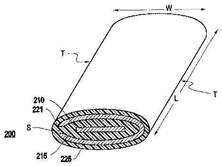
Figures 2A-2F illustrate various aspects of an electrical wire 200 according
to the
exemplary embodiments of the present invention;
Figures 3A-3W illustrate various possible conductor configurations in the
electrical
wire 200 according to the exemplary embodiments of the present invention;
Figures 4A-4C illustrate an aspect of the electrical wire 200 having a hot
zone 295
according to the exemplary embodiments of the present invention therein;
Figures 5 illustrates another aspect of the electrical wire 200 according to
the
exemplary embodiments of the present invention therein;
10d
CA 02537825 2006-08-25
WO 2005/024849 PCT/US2004/028972
Figure 6 illustrates a possible termination configurations for the electrical
wire 200
according to the exemplary emboidments of the present invention therein;
Figure 7 illustrates an electrical wire that can be considered as forming a
series of
capacitors with an equivalent capacitive circuit according to the exemplary
embodiments of
the present invention;
Figures 8-10 provide schematic illustrations of a typical two plate capacitor,
four plate
capacitor and three plate capacitor, respectively, according to the exemplary
aspects of the
present invention; and
Figures 11-12 illustrate how capacitively coupled current may be cancelled in
the
electrical wire, according the exemplary aspects of the present invention;
Figure 13 provides a schematic diagram of an exemplary configuration for
detecting
ground loop continuity using the electrical wire, according to the exemplary
aspects of the
present invention;
Figure 14 provides a conceptual illustration for providing split ground
signaling,
according to the exemplary aspects of the present invention;
Figure 15 illustrates a method 1500 of fabricationg an electrical wire
according to the
exemplary aspects of the present invention; and
Figures 16-17 provide exemplary configurations of the electrical wire 200
according
to the exemplary aspects of the present invention.
DETAILED DESCRIPTION OF EXEMPLARY EMBODIMENT OF THE
INVENTION
Referring now to the drawings, and more particularly to Figures 2A-17, the
present
11
CA 02537825 2006-08-25
WO 2005/024849 PCT/US2004/028972
As illustrated in Figure 2A, an the exemplary embodiment of present invention
is directed to
an electrical wire 200 including at least one electrifiable conductor 210, and
first and second
return conductors 221 which are respectively formed on opposing sides of the
at least one
electrifiable conductor 210, such that the at least one electrifiable
conductor is at least
substantially entrapped by the first and second return conductors 221. The
wire 200 may also
include a first insultating layers 215 and second insulating layers 225.
It should be noted that unless otherwise noted, any of the layers (e.g.,
conductors,
insulating layers, etc.) in the present invention and discussed herein may be
formed of a plurality
of layers. Thus, for example, insulating layer 215 should be construed as at
least one insulating
layer 215, an electrifiable conductor should be construed to mean at least one
(e.g. a plurality of)
electrifiable conductors, and so on.
The electrical wire may be used for a basically unlimited range of voltage
applications
(e.g., OV to 240 V and higher). For example, the wire may include a Class 1 or
Class 2 capability
and other low voltage/current capabilities, and may be used for commercially
available utility
voltages such as 120V AC and 240V AC, and may be used for other applications
other than
Class 1 or Class 2, or these commercially available voltages.
As illustrated in Figure 2B, the electrical wire 200 may have a longitudinal
(e.g.,
lengthwise) direction, L, and a transverse (e.g., widthwise) direction, W.
These directions may
also be referred to as a horizontal dimension of the wire. The wire may futher
be considered as
having a thickness (e.g., a total thickness of all of the stacked layers)
which may be referred to as
a vertical dimension.
12
CA 02537825 2006-08-25
WO 2005/024849 PCT/US2004/028972
The wire 200 may also include terminal portions (e.g., terminations) (e.g.,
not illustrated
in Figure 2B) formed at the ends of the wire 200 in the longitudinal
direction,. For example, one
end (e.g., terminal portion) of the wire 200 may be connected to a source
module (e.g., power
source, voice/data transmission source, etc.) and the other end (e.g.,
terminal portion) may be
connected to a destination module (e.g., swithc, outlet, electronic device
etc.). It should be noted
that the present invention does not necessarily include any particular form
termination (e.g.,
current source, earth ground, etc.) but may include a longitudinal portion of
wire formed between
two termination points.
As further illustrated, the first and second return conductors 221 are formed
such that the
at least one electrifiable conductor is at least substantially entrapped (e.g.
enveloped,
surrounded, encased) by the first and second return conductors. By
"substantially entrapped" it is
meant that for all practical purposes, the electrifiable conductor 210 cannot
be contacted with a
foreign object (e.g., a nail, screw, staple, etc.) without first touching the
one of the return
conductor 221. The term "substantially entrapped" does not necessarily mean
that the return
conductor 221 completely surround the electrifiable conductor (although such a
design is
possible). Instead, it means that any distance between the return conductors
and the electrifiable
conductor (e.g., the thickness of an insulating layer between the
electrifiable conductor and a
return conductor) is so small (e.g., about 0.030" or less) that such foreign
object cannot
reasonably go between the return conductors and the electrifiable conductor
without touching the
return conductors.
For example, as illustrated in Figure 2B, the electrical wire 200 may be
formed of layers
(e.g., substantially flat layers) having a stacked configuration. At least
some of these layers (e.g.,
13
CA 02537825 2006-03-03
WO 2005/024849 PCT/US2004/028972
return conductor 221, insulating layers 215, 225) may be brought together
(e.g., mated together
by crimped, bonded, etc.) along the longitudinal edges, T, of the wire 200.
It is important to note that there may remain a distance, S, between the
return conductor
layers 221. That is, the electrifiable conductor 210 does not have to be
completely entrapped by
the return conductors 221. The inventors have determined that so long as any
distance between
the return conductors and the electrifiable conductor (e.g., the thickness of
an insulating layer
between the electrifiable conductor and a return conductor) is sufficiently
small (e.g., about
0.030" or less) an object cannot likely penetrate the wire 200 and contact the
Electrifiable
conductor 210 without first contacting the return conductor 221.
Further, the electrifiable conductor is at least "substantially entrapped"
along the
longitudinal portion of the wire. That is, at the terminal portions of the
wire 200, the electrifiable
conductor may be exposed and not entrapped, for connection to a device (e.g.,
a source or
destination module).
It should also be noted that the term "Electrifiable" is intended to mean
having a
capability (e.g., purpose) of connecting to a source or electrical current and
carrying (e.g.,
delivering) an electrical current or electrical signal (e.g., an AC or DC
power supply or an
electrical communication signal such as a voice or data transmission signal).
An Electrifiable
conductor may be referred to as the "non-return conductor". An Electrifiable
conductor may also
be referred to as a "hot conductor". Further, the term "return" is intended to
mean having a
purpose of returning an electrical current (e.g., not having a purpose of
delivering an electrical
current or electrical power supply to a load). A return conductor may also be
referred to as a
grounded conductor or a neutral conductor.
14
CA 02537825 2006-03-03
WO 2005/024849
PCT/US2004/028972
Specifically, an "electrifiable" conductor may be considered any conductor
within the
"hot zone" as defined herein. The electrifiable conductor (e.g., a conductor
in the hot zone) may
be the "hot" conductor in operation but not necessarily. For example, with
regards to a 3-way
switch, the electrifiable conductor (e.g., a conductor in the "hot zone") may
in one condition, act
as a hot conductor, but in another condition act as a ground conductor.
In addition, the term "grounding" is intended to mean having a capability or
purpose of
connecting to "earth ground". A grounding conductor may also be referred to as
simply a
"ground conductor". The grounding conductor is not intended to have any return
current on it.
Further, the term "conductor" is defined to mean a conductive medium which is
capable of
carrying an electrical current.
Figures 2C-2D illustrate another exemplary embodiment of the present
invention. In the
exemplary aspect which is illustrated in Figure 2C, the electrical wire 200
includes at least one
first conductor 210 which is Electrifiable, at least one return conductor 221
and at least one
grounding conductor 222.
In this aspect, the wire 200 may also include a first insulating layer 215, a
second
insulating layer 225, and a third insulating layer 230. As illustrated in
Figures 2C, the first
insulation layer 215 may be formed between the at least one Electrifiable
conductor 210 and the
at least one return conductor 221, the second insulation layer 225 may be
formed between the at
least one return conductor 221 and the at least one grounding conductor 222,
and the third
insulation layer 230 may be formed on the at least one grounding conductor
222.
Figure 2D illustrates an exploded view of an exemplary aspect of the
electrical wire 200.
As illustrated in Figure 2D, the conductors of the electrical wire 200 may
have a stacked
CA 02537825 2006-03-03
WO 2005/024849 PCT/US2004/028972
arrangement. The electrical wire 200 may also include an adhesive 290 for
bonding adjacent
insulation layers and conductors in the electrical wire.
It should be noted that the drawings are intended to be illustrative. In the
actual electrical
wire of the present invention, there may be no visible spacings (e.g., the
white areas in Figure
2D) between the conductors, insulation, and adhesives components, each of
which is described
further below.
Figures 2E-2F illustrate additional exemplary aspects of the electrical wire
200. For
example, in the exemplary aspect of Figure 2E, the conductors 210, 221, 222
may include
substantially circular-shaped conductors (e.g., coaxially arranged). In the
aspect of Figure 2F, the
conductors 210, 221, 222 may include substantially oval-shaped conductors.
In general, the electrical wire of the present invention (e.g., protective
layered wire)
provides an alternative which can be applied in a variety of ways and in a
variety of locations and
represents a paradigm shift for all other electrical wire systems. The
electrical wire may include
protective layered wire which can have conductors with a parallel longitudinal
axis (e.g.,
conductors having a curvilinear cross-section), or the wire may be
substantially stacked in nature,
such that each conductor has a substantially parallel plane (e.g., parallel
axis). However, the
conductor cross-section is not necessarily coincidental (e.g., concentric) or
coaxial.
For example, in one aspect, an inner (hot) conductor is surrounded or bounded
by an
insulator, then an intermediate (neutral) conductor, a second insulator, then
an outer (grounding)
conductor, and an outer insulator.
The exemplary embodiments of the electrical wire can have cross-sectional
shapes
ranging from a substantially curvilinear geometry such circles (e.g.,
concentric circles), ovals,
16
CA 02537825 2006-03-03
WO 2005/024849 PCT/US2004/028972
ellipses, or flat (e.g., linear or rectilinear) layers. The concentric format
(e.g., Figure 2E) (e.g.,
major and minor axes approximately equal) is symmetric with an innermost
conductor (e.g.,
hot/Electrifiable) having relatively small surface area. The oval or ellipsoid
format (e.g., Figure
2F) (e.g., major and minor axis unequal) supports a relatively flat innermost
conductor. The flat
format (e.g., Figures 2B-2D) (major axis = 1, minor axis = 0) supports all
flat conductors and
insulators (e.g., multi-planar flat conductor wire).
The exemplary embodiments of the electrical wire may offer differing
advantages
regarding safety, application methodology, cost, and ease of manufacture. The
concentric and
oval formats may have exceptional safety aspects (e.g., a very low penetration
hazard). Whereas,
the flat format has an exceptional current carrying capability due to a large
surface area of each
conductor and would likely trip any safety disconnect device (e.g., breaker,
GFCI, etc.) in any
case of penetration. Further, the use of the electrical wire (e.g., protective
layered wire) is
advantageous from a number of points of view including safety, electrical
interference shielding,
and flammability.
Regarding the risk of electrocution, the inevitable issue centers around
penetration of an
electrified conductor (e.g., an electrifiable conductor) by objects such as
nails, screws, drill bits,
etc. Traditional in-wall and in-ceiling wiring has the potential for
penetration by any of the
aforementioned objects with a possibility of electrocution as a result.
Although the electrical wire of the present invention may be surface mounted
(e.g., on a
wall or ceiling, or on a floor such as under a carpet) it has the distinct
advantage over
conventional wire by assuring that the penetrating object first passes through
at least one non-
Electrifiable conductor (e.g., a return conductor and/or a grounding
conductor) prior to any
17
CA 02537825 2006-03-03
WO 2005/024849 PCT/US2004/028972
contact with the Electrifiable (e.g., hot/innermost) conductor. Thus, as the
penetration motion
proceeds, high currents on hot through the ground and neutral are generated
causing a circuit
breaker to expeditiously trip.
Specifically, with respect to this penetration dynamics solution of the
electrical wire (e.g.,
stacked electrical wire), to reduce the chance for electrification of a
penetrating object, conductor
thickness of the Electrifiable conductor (e.g., hot conductor) should be low
(e.g., as low as
possible) relative to the total thickness of the outer layers (e.g., grounding
conductors and return
conductors). A good layer thickness ratio, R, of 1.00 has been demonstrated
through test results,
whereby R = (TG+TN)/TH = 1.00, where TG, TN, and TH are the conductor
thickness of the
Grounding, Grounded, and Electrifiable conductors, respectively, and R is the
Layer Thickness
Ratio. For example, in one exemplary embodiment, the thickness of the
grounding and return
conductors was 0.001", and the thickness of the Electrifiable conductor was
0.002, such that the
ratio R= (TG+TN)/TH = (0.001" + 0.001")/0.002" = 1.00.
Further, in the penetration dynamics of the electrical wire, the opposing
Grounded and
Grounding layers may also contribute favorably to the ratio, R, resulting in a
safer condition. It
has been shown that the higher this ratio, R, is, the safer the wire is during
a penetration with a
conductive object such as a nail.
During the short circuit, the electrical wire may act as a voltage divider
from the source to
the point of penetration. The layer thickness ratio produces a ratio-metric
scaling of the voltage
that is applied from within to the penetrating object. Therefore, the safer
condition results from
the lower voltage at the nail, etc.
During a penetration to increase the probability of actuation and to decrease
the actuation
18
CA 02537825 2006-03-03
WO 2005/024849 PCT/US2004/028972
time of a safety device (e.g., circuit breaker, circuit interrupter (e.g.,
GFCI) or other safety
disconnect device), the conductor thickness of the outer (e.g., grounding and
return conductors)
layers must be substantial enough to cause a reliable short circuit at the
point of penetration. The
short circuit must result in high currents that cause the safety devices to
trip at their fastest
response time. This results in a safer condition based on time. The
combination of lower voltage
and shorter time produces a significantly safer condition than either
condition by itself.
At the point of penetration, after the safety device has removed from the
power supply, it
can be assumed that all layers remain in a relatively low resistance
relationship. This is due to the
presence of the penetrating object and/or the insulation displacement damage
of the various
layers. Furthermore, the flashpoint of the penetration may cause somewhat of a
melded or fused
area in the perimeter of the penetration. With repeated application of power
into the damaged
area, the perimeter may increase (e.g., especially if the penetrating object
has been removed) in
size but sufficient resistance will be residual enough to repeat reactivations
of the safety device
upon being reset.
The way to avoid repeated application of power into the damaged area could be
to have a
circuit within an Active Safety Device (ASD) that can detect a substantially
shorted return to
grounding conductors prior to applying power to the electrical wire. This
feature capability is
supported by the design of the electrical wire.
Therefore, the electrical wire (e.g., protective layered wire) of the present
invention can
be considered inherently safe with a circuit breaker or fuse. In addition, the
safety can be further
improved when the wire is used in conjunction with a safety device (e.g.,
circuit breaker, circuit
interrupter (e.g., ground fault circuit interrupter (GFCI)) or other safety
disconnect device).
19
CA 02537825 2006-03-03
WO 2005/024849 PCT/US2004/028972
The exemplary embodiments of the present invention also provide advantages
with
respect to other electrical safety issues, such as frayed insulation allowing
incidental contact and
possible electrocution are better solved by the exemplary embodiments of the
present invention
(e.g., protective layered electrical wire) in that it may include three layers
of insulation between
the hot conductor and the outside world (in any direction). This is commonly
referred to as
"triple- insulated" as opposed to contemporary double-insulated conventional
wire.
Regarding electrical shielding, the outer grounding layer of the electrical
wire of the
present invention (e.g., protective layered wire) may provide a shield whereby
power
transmission signals or load-generated electrical noise cannot pass through
the cable to interfere
with broadcast signals or to cause "hum" in audio equipment.
In addition, regarding flammability, the electrical wire of the present
invention offers
several advantages over conventional electrical wires and wiring systems.
Specifically, the
electrical wire of the present invention may provide a relatively large
surface area for dissipating
heat. Thus, the outer conductor(s) (e.g., return and grounding conductors) may
easily conduct
heat away from film insulation being heated from an external source, reducing
the risk of fire
caused by the heat. Further, the rate of heat transfer may exceed the
combustion rate, thus
quenching a localized combustion area.
Additional "layers of protection" can be added to the electrical wire of the
present
invention. For example, in addition to an electrical wire (e.g., protective
layered wire) and circuit
breaker configuration, a GFCI, arc fault detector, and specially developed
"active safety devices"
may also be included and used with the electrical wire to further reduce the
probability of shock,
electrocution or fire.
CA 02537825 2006-03-03
WO 2005/024849 PCT/US2004/028972
In addition, since the Electrifiable conductor in the present invention may be
provided
between (e.g., within) the return and grounding conductors, the return and
grounding conductors
and the insulation layers may provide abrasion protection for the
Electrifiable conductor. That is,
the layers formed on the electrifiable conductor (e.g., insulation layers,
return conductor and
Further, the electrical wire of the present invention may include a flat,
flexible, wire that
allows the user to bring electricity to any area of a wall or ceiling in a
room. The electrical wire
may be very thin (e.g., having a total thickness of no more than 0.050 inches)
and can be
Each of the conductors in the electrical wire of the present invention may
include one or a
plurality of conductive layers (e.g., conductive copper, aluminum or other
conductive material
The conductors may be formed of a variety of materials and have a variety of
patterns,
dimensions and spacings. For example, the conductors may be formed of an
electrically
conductive material such as metal (e.g., copper, aluminum, silver, other
conductive materials,
The conductor thickness should be consistent across its length and width,
thereby
21
CA 02537825 2006-03-03
WO 2005/024849 PCT/US2004/028972
eliminating any resistance "hot spots". The current carrying specifications of
a particular
application may be accomplished in any of three ways, either individually or
in combination.
First, the width of the conductors may be varied. Second, additional thin
conductive layers (e.g.,
copper, aluminum or other conductive material) may be stacked for each
conductor. Third, the
thickness of the conductor may be increased.
For example, in one exemplary load and current application, each conductor may
include
about two conductive layers (e.g., copper, aluminum or other conductive
material layers). It is
understood, however, that utilizing more or less layers, for each of the below
disclosed
embodiments, is within the scope of the invention.
The insulating layers in the electrical wire may be formed of a variety of
materials. For
example, the insulating layers may include a polymeric material (e.g.,
polypropylene film,
polyester film, polyethylene film, etc.). Further, the insulating layers may
have a thickness, for
example, in a range of 0.00025 to 0.030 inches.
The insulation layers formed between the conductors may also orient the
conductive
layers. In addition, the insulation material may be used alone, or in
combination with the internal
adhesive, to separate the conductors and maintain a safe distance between
conductors of different
purposes (e.g., grounding vs return or Electrifiable (e.g., hot)). Further,
the electrical wire may
have tapered edges (e.g., tapered in a transverse width direction) to
facilitate the optical occlusion
(e.g., when mounted on a ceiling or wall). For example, the layers (e.g.,
conductor layers and/or
insulation layers) may have different widths to facilitate such a tapered
edge.
It is understood that additional insulative materials are considered to be
within the scope
of this invention and maybe used so long as the insulation is compliant,
paintable, and bondable
22
CA 02537825 2006-03-03
WO 2005/024849 PCT/US2004/028972
to surfaces. The insulation should also be compatible with concealing (e.g.,
joint) compounds, be
UV tolerant, and have similar thermal expansion and contraction
characteristics as that of the
conductors and the surface to which it is adhered.
Other desirable properties are that the insulation should withstand tensile
forces applied
in the fabrication process, not retract or relax under storage conditions, and
be removable when
its use is completed. Any abrasion, cracking, cutting, piercing, or any other
insulation damage
(e.g., damage that would render an unsafe exposure to bodily harm or damage,
or physical or
construction damage, such as to a structure) will be made safe using
electronic means of failure
detection that will disconnect potentially harmful or damaging currents from
the user in a time
frame that will prevent permanent harm.
Further, adhesive material 290 (e.g., Figure 2D) should be able to bond to the
insulation
layers and the conductors. For example, adhesive tape, liquid adhesive,
thermal adhesive,
pressure-sensitive adhesive or UV sensitive adhesive or a combination of any
such adhesives or
adhering methods, may be used as an internal adhesive. The internal adhesive
material may also
function to separate the conductive layer groups and maintain a safe
dielectric distance between
conductors of different purposes.
An external adhesive layer may also be formed on the outermost insulating
layer of the
electrical wire, for adhering the wire to a desired surface. The external
adhesive layer could be,
for example, two-sided tape, with one side being fixed to the back of the wire
and the other to the
wall (or ceiling) or surface. Alternatively, a chemical adhesive may be
applied separately, and
may consist of any of the adhesives with good bonding qualities to both the
insulation layer and
the desired surface to which the wire is adhered. Insulating layers may also
be joined by
23
CA 02537825 2006-08-25
WO 2005/024849 PCT/US2004/028972
mechanical deformations and thermal fusing without the addition of any
adhesive.
Referring again to the drawings, Figures 3A-3W illustrate cross-sectional
views of
possible configurations of the electrical wire 200 according the exemplary
aspects of the present
invention (for simplicity, the insultating layers are not identified in
Figures 3A-3W).
Fore example, the wires of Figures 3A and 3M are similar to the wires of
figures 2B and
2C, respectively. As shown in Figures 3B, 3E, 3N, the conductros may have a
staggered
arrangement and may include non-uniform widths (e.g., in a transverse
direction).
As illustrated in Figure 3C, the conductors (e.g., hot conductor 210 may be
folded
over on themselves). Further, as illustrated in Figure 3D, another conductor
(e.g., return
conductor 221) may be folded over a folded conductor (e.g., Electrifiable
conductor 210).
As illustrated in Figure 3F, the conductors may be treated (e.g., thermally,
chemically or
mechanically) or bonded by some manner on a side. For example, in Figure 3F,
an upper
conductor 222 is joined (e.g., stitching, seam welding, chemical bonding, or
other mechanical
means) to a lower conductor 222. This may be used to provide a more protective
barrier along
the longitudinal edges of the electrical wire, making it more difficult for an
object to penetrate
the electrical wire and contact the electrifiable conductor from such
longitudinal edge.
Figure 3G-3I illustrates a wire in which a conductor 210 has a round shape
whereas
conductors 221 and 222 are wave-shaped or substantially flat. Further, Figures
3J-3L illustrate a
wire in which the conductors may each be bent such that they are formed in
more than one plane.
For example, in Figure 3J, the conductor 221 has a bent configuration for
substantially
surrounding the conductors 210.
Figures 30 and 3S illustrate a wire in which a conductor 210 has a
substantially oblong
24
CA 02537825 2006-03-03
WO 2005/024849 PCT/US2004/028972
(e.g., oval) shape, whereas the other conductors 221, 222 may be substantially-
flat or bent. In
Figures 3P-3R, and 3T, some of the conductors may be substantially-flat and
other of the
conductors may be formed around (e.g., partially around) the flat conductor.
Further, as
illustrated in Figures 3U-3W, the conductors (e.g., conductors 210 in Figure
3U) may be bent
around each other in an interlocking manner.
Figures 4A-4C illustrate another exemplary aspect of the electrical wire
according to the
present invention. These drawings describe the "hot zone" which is an
important concept
introduced by the present invention. Specifically, the "hot zone" may be
considered as a zone
which is at least "substantially entrapped" by a return conductor. As
illustrated in Figure 4A, the
hot zone may include layer segments arranged in any horizontal and vertical
format, depending
upon the application(s) of the electrical wire.
For example, Figure 4A illustrates a cross-sectional view of a general case
for a
conductor orientation. It should be noted that the insulating layers (and
adhesive) are not shown
in Figures 4A-4C for simplification.
As shown in Figure 4A, the electrical wire 200 may include grounding
conductors 222
and return conductors 221 formed on opposing sides of (e.g., above and
beneath) the hot zone
295. Moreover, in the hot zone 295 is included "M" vertical segments, and "N"
horizontal
segments of Electrifiable conductors. More specifically, the hot zone 295 may
include segment
(1,1) 296, through segment (1,M) 297, and segment (N,1) 298 through segment
(M,N) 299. It
should be noted that M and N are not particularly limited.
In addition, an application of the wire according to the exemplary aspects of
the present
invention may include transmission of electrical communication signals such as
voice and data
CA 02537825 2006-08-25
WO 2005/024849
PCT/US2004/028972
transmission signals. For example, the wire may be used as part of power line
carrier (PLC)
communication system in which the wire (e.g., a portion of the wire) is used
to provide AC
electrical power, and is also used (e.g., a portion of the wire is used) as a
network medium to
transmit voice and/or data communication signals. Thus, the wire may be used
to provide high
speed network access points wherever there is an AC electrical outlet.
Specifically, the wire may transmit electrical communicaiton signals during
the time
proximity of zero-crossing of an AC power supply. In addition, there can be
many different types
(e.g., formats) of communication signals transmitted by the wire including
RS485, HDTV,
etc., according to the present invention.
For example, as illustrated in Figure 4A, the electrical wire 200 may also
include a
portion 450 which may be reserved for an elecrical signal (e.g., a
communications signal) in
addition to an electrical power being supplied elsewhere by the "hot zone".
For example, the
conductors in this reserved portion 450 may include patterned conductors such
as those described
in McCurdy, et al., U.S. Patent No. 6,688,912 (NON-UNIFORM TRANSMISSION LINE
AND
METHOD OF FABRICATING THE SAME) which was filed on May 28, 2002 and published
on
December 4, 2003. Application and is incorporated by reference herein.
Further, the wire 200 may
include a plurality of such portions 450 which may each be dedicated to
carrying the same or
different types (e.g., formats) of communication signals.
It should be noted that the electrical wire according to the exemplary aspects
of the present
invention may be used for transmitting communication signals independently of
any electrical
current. that is, the Electrifiable conductors may be dedicated entirely to
communication signals or
entirely to an electrical power supply.
26
CA 02537825 2006-03-03
WO 2005/024849 PCT/US2004/028972
For 3-way switching of lights there may be a need for two conductors in the
hot zone that
will alternately be switched from return to electrified (e.g., neutral to
hot). Figure 4B illustrates
two possible embodiments to accomplish this with the present invention.
For example, the first embodiment (on the left) includes return conductors 221
and
It should be noted that the first embodiment provides an electrical wire with
a smaller
Further, Figure 4C illustrates an electrical wire 200 according to another
exemplary
This aspect may be used, for example, for multiple branch circuits. It should
be noted that
the horizontal segments may share a common insulator between layers and on the
outside of the
grounding conductors 222.
20 Referring again to the drawings, Figure 5 illustrates another exemplary
aspect of the
electrical wire 200 of the present invention. (Note that the wire of Figure 5
is similar to that in
Figure 2D). As shown in Figure 5, the electrical wire 200 may include 14 AWG
(e.g., American
27
CA 02537825 2006-03-03
WO 2005/024849 PCT/US2004/028972
Wire Gauge) electrical wire. For example, an adhesive 290 may be included as
illustrated.
Further, the wire 200 may include insulating layers 215, 225 and 230 which are
formed of
polyester and which are 0.001 inches thick, fully annealed. The wire 200 also
includes
conductors 210, 221 and 222 which are formed of copper (or aluminum or other
conductive
material) CDA 102 or CDA 110, having a thickness of 0.001 inches.
As is evident from Figure 5, the widths of the layers vary. For example, the
conductor
210 has a width of 1.620 inches, whereas conductors 221 and 222 have a width
of 1.750 inches.
Insulating layer 215 has a width of 2.000 inches, insulating layer 225 has a
width of 2.250 inches
and insulating layer 230 has a width of 2.500 inches.
The electrical wire according to the exemplary aspects of the present
invention may
include a longitudinal portion formed between two terminal portions. Figure 6
illustrates
possible terminations for the electrical wire 200.
The line side 610 in Figure 6 is where power originates and the load side 620
is where it
is delivered. The line side power may typically originated via a common
receptacle or other
source (e.g., a conventional source). Termination techniques (e.g., at either
end of the wire) can
include soldering, crimping, surface contact, clamping and insulation
displacement.
With respect to the line side terminations, a male plug placed in the
receptacle with a tail
of power cord can be terminated within the line side termination box 615. In
this case, the box
may be mounted on the wall (or ceiling) near the outlet receptacle. Further,
the termination box
can be a "source module" as a mechanical interface to an active safety device
(ASD), which
plugs into the outlet. In addition, the termination box can reside over the
outlets and plug into an
outlet (receptacle).
28
CA 02537825 2006-03-03
WO 2005/024849 PCT/US2004/028972
With respect to the load side terminations, a set of three "flying heads" or
conventional
wires may be provided for the user to cut-to-length and terminate as needed
(e.g., sconce lights,
ceiling fans, etc.). Further, a terminal strip mounted on a small printed
circuit board that is
attached to the wire can provide screw terminals to the user. In addition, the
load side
termination (destination) box 625 can include outlets of its own for the user
to plug.
Another aspect of the wire according to the exemplary aspects of the present
invention, is
that it may provide a capacitance solution. That is, the capacitance resulting
from the
Electrifiable conductor which may be in close proximity to the return
conductor, may represent a
reactive current in superposition with any load current. This capacitance is
charged based on the
applied voltage (e.g., AC or DC). Since the return conductor has a low voltage
relative to the
Electrifiable conductor, very little charge will be accumulated within any
capacitor formed
between the return and grounding conductors.
Specifically, the electrical wire (e.g., layered FlatWire) can be considered
as forming a
series of capacitances (e.g., capacitors) with an equivalent circuit (e.g.,
capacitive circuit) as
illustrated in Figure 7. As shown in Figure 7, the electrical wire 200
including an Electrifiable
conductor 210, grounding conductors 221 and grounding conductors 222 may form
capacitors
Cl, C2A and C2B.
In this case, capacitor Cl is a parallel plate capacitor formed by the return
conductor 221
(e.g., neutral layer(s)) in close proximity to the Electrifiable (e.g., inner
(hot)) conductor 210.
Capacitor C2 is formed by return (e.g., neutral) conductor 221 and grounding
conductor 222 in
close proximity.
With respect to the impact of the capacitors Cl and C2, it should be noted
that capacitor
29
CA 02537825 2006-03-03
WO 2005/024849 PCT/US2004/028972
Cl (C1A/C1B) may cause a current to flow between the Electrifiable conductor
(e.g., FlatWire
hot) 210 and return conductor (e.g., FlatWire neutral) 221 via the dielectric
(and any air that may
be present with the absence of adhesive) formed therebetween. Thus, it can be
seen that any air
that remains trapped between layers after the final fixation (e.g. concealing
compound,
wallpaper, paint, etc.) of the electrical wire 200 (e.g., FlatWire) may cause
a dramatic reduction
in capacitance due to air's low dielectric constant (6 = 1.0). As the
longitudinal (e.g., lengthwise)
distance of the wire increases, a significant capacitance in the electrical
wire 200 (e.g., AC
FlatWire) can be created and, therefore, relatively large currents can be
produced.
Further, the current from capacitor Cl, being on the return (e.g., neutral)
conductor 221
and Electrifiable (e.g., hot) conductor 210, represent a balanced load current
to H-N CTs (e.g.,
return current flow minus hot current flow is zero) and therefore are not
considered to be a
problem regarding line source GFCI false tripping. In case the capacitive
current on return and
Electrifiable conductors (e.g., neutral and hot) should become a problem, a
"cancellation" circuit
may be implemented to null out the current.
Further, capacitor C2 (C2A/C2B) will not cause a significant current to flow
between the
return (e.g., neutral) conductor 221 and Electrifiable (e.g., hot) conductor
210 (e.g., FlatWire
neutral and FlatWire Gnd) since the voltage differential is typically less
than 1 volt. Further, as
noted above, in case the capacitive current on the return and Electrifiable
conductors, (e.g,.
neutral and hot) ever become a problem, a "cancellation" circuit (e.g., a
circuit having an
inductance) may be implemented to null out the current.
Referring again to the drawings, the capacitance value of the capacitor CIA
may actually
be derived from a parallel plate capacitor model. Figures 8-10 illustrate a
typical two plate
CA 02537825 2006-03-03
WO 2005/024849 PCT/US2004/028972
capacitor, four plate capacitor and three plate capacitor, respectively, where
P identifies the
capacitor plates, and D identifies the dielectric between the capacitor
plates.
The parallel plate capacitance, C, (e.g., as indicated by a capacitance meter,
C meter) may
be given by C = sA/d, where the dielectric constant of the dielectric, D,
between the conductors
is given as 6 = Co=ER , where A is the area of the plate capacitor, d is the
distance between plate
surfaces, so is the dielectric constant (e.g., permittivity) of free space,
and sR is the relative
permittivity of the dielectric material.
Thus, as illustrated in Figure 8, for a two plate capacitor, the area, A, of
the parallel plate
capacitor is given as A= L=W, and where L is the Length of the plate, W is the
width of the plate,
and as illustrated in Figure 9, for a four plate capacitor, the area, A, is
given as A= L=W=2
Figure 10 shows the wiring/configuration of a 3-plate capacitor stack that
emulates the
electrical wire 200 (e.g., electrical FlatWire) with shorted shields relative
to each Electrifiable
(e.g., inner) conductor. It should be noted that the configuration of Figure
10 may be derived by
eliminating 1 plate (e.g., conductor) and 1 dielectric separator (e.g.,
insulating layer) from the
structure shown in Figure 9. ,
Further, as illustrated in Figure 10, the area A of the plate capacitor is
given as A=W=L=k,
where the plate multiplier constant, k, is actually the number of plates (n)
divided by 2. Thus, for
a three plate capacitor, the constant k = 1.5.
Therefore, for the electrical wire (e.g., stacked electrical FlatWire) the
capacitance for the
capacitor formed between the Electrifiable conductor and its two adjacent
return conductors (e.g.,
layers), is given as C = s( W = L = 1.5 )/d, or C = 1.5 =W =L =s/d.
It should be further noted that the capacitance value calculated using the
above equation
31
CA 02537825 2006-03-03
WO 2005/024849 PCT/US2004/028972
turns out to be worst case since the conductors (e.g., layers) are not
necessarily in full contact
with each other. Air spaces and gaps where no adhesive is present produce
larger values of "d"
thus causing smaller values of capacitance. This capacitance may vary based on
the percent of
surface adhesion between layers and the amount of compressive force that may
be applied to the
outer surfaces of the electrical wire (e.g., FlatWire)
Referring again to the drawings, Figures 11-12 illustrate how capacitively
coupled
current may be canceled in the electrical wire according the exemplary aspects
of the present
invention. Specifically, Figure 11 illustrates the case where the electrical
wire 200 having an
Electrifiable conductor 210 and two return conductors 221, is terminated at an
active safety
device (ASD) or source module 1100.
In this case, the capacitively coupled current, CC, can be represented as
shown in Figure
11. Since the return conductor (e.g., neutral) is not sigificantly electrified
(e.g., low AC volts) it
has little impact on current coupled to the shields. The Electrifiable
conductor (e.g., hot) 210
however, is highly electrified and is coupling capacitive currents into the
ground conductors 221
(e.g., neutrals) throughout the length of the electrical wire (e.g.,
flatwire).
Figure 12 provides a capacitive current cancellation diagram which illustrates
how a
cancellation circuit might be used to produce a net zero current on the
Electrifiable conductor
210 and ground conductors (e.g., hot and neutral conductors) regarding
capacitance. As
illustrated in Figure 12, the cancellation circuit 1200 may be included as
part of or used in
conjunction with an active safety device 1100.
Specifically, the current, IL after application of the cancellation circuit
1200 may be given
by IL=INI + 1N2 ¨ lc, where 'Ni and 1N2 are the current on the return
conductors 221, and Ic is the
32
CA 02537825 2006-03-03
WO 2005/024849 PCT/US2004/028972
cancellation current (e.g., provided by the cancellation circuit). For
example, IL may be OmA.
Another aspect of the electrical wire according to the exemplary embodiments
of the
present invention, is a hi-directional nature of the "shielding" capability of
the grounding (e.g.,
outer; earth ground) conductors. For example, as noted above, the at least one
grounding layer
inhibits power transmission signals and load-generated electrical noise from
being
transferred/emitted from the electrical wire. In addition, the shielding
provided by the grounding
conductors prevents ingress of externally generated electrical noise onto
either the return or
Electrifiable conductors, which is also a valuable feature.
Also in the interest of safety and communications regarding grounding layers,
the two or
more grounding conductors 222 (e.g., isolated (outer) grounding layers) in the
electrical wire
(e.g., stacked arrangement) provide an opportunity to send a communication
type signal
longitudinally to the other end of the grounding conductor 222, through a
wired "jumper" at the
destination "module" and returned longitudinally to the source. This may be
used to provide, for
example, a "ground loop continuity check".
Thus, the electrical wire may provide the ability to check for continuity by
an "Active
Safety Device" prior to electrifying the Electrifiable conductor or segments
of the Electrifiable
conductor. One practical application for this feature is for providing safety
while an electrician
terminates exposed destination ends of the electrical wire.
Figure 13 provides an schematic diagram of an exemplary configuration for
detecting
ground loop continuity using the electrical wire. As illustrated in Figure 13,
the grounding
conductor 222 and opposing grounding conductor 222 may be considered as part
of a closed loop
between a source 1310 and destination 1320.
33
CA 02537825 2006-03-03
WO 2005/024849 PCT/US2004/028972
The wire may also accommodate additional communication tasks such as providing
a
transmitting current transformer (CT) and a sensing current transformer (CT).
A periodic signal,
which may be (e.g., preferably) greater than AC line frequency, may be
injected onto one of the
grounding conductors 222 while the opposed grounding conductor 222 is sensed
for signal return
via the sensing CT.
Figure 14 provides a conceptual illustration for providing split ground
signaling where
the electrical wire is disposed between a source module (e.g., current tap)
1410 and a destination
module 1420, which may transmit and receive electrical signals processed by
transmit and
receive electronics. The two or more return conductors 222 (e.g., isolated
(outer) grounding
layers in the stacked or lateral (planar) arrangement) can be further split or
separated transversely
to provide an opportunity to send a communication type signal longitudinally
and differentially
between the split conductors.
Referring again to the drawings, Figure 15 illustrates a method 1500 of
fabricating an
electrical wire according to the exemplary aspects of the present invention.
The method 1500
includes forming (1510) at least one electrifiable conductor, forming (1520) a
pair of return
conductors on opposing sides of the at least one electrifiable conductor, such
that the at least
one electrifiable conductor is at least substantially entrapped by the return
conductors.
Specifically, the conductors in the electrical wire (e.g., the Electrifiable,
return and
grounding conductors) may be formed of a substantially conductive medium, and
may include,
for example, copper, aluminum, steel, silver, gold, platinum, nickel, tin,
graphite, silicon, an
alloy including any of these, conductive gas, metal, alloy metal. That is, the
conductors may
include any material that is able to transfer electrons regardless of
efficiency in doing so. This is
34
CA 02537825 2006-03-03
WO 2005/024849 PCT/US2004/028972
true as long as the relative ability to transfer electrons in the "conductors"
is substantially better
than the "insulators".
Further, the insulating layers may be formed of substantially non-conductive
mediums
("insulators"), and may include, for example, a material that is organic,
inorganic, composite,
metallic, carbonic, homogeneous, heterogeneous, thermoplastic (e.g. poly-
olefin, polyester,
polypropylene, polyvinyl chloride (PVC)), thermoset, wood, paper, anodic
formation, corrosive
layer, or other.
The insulating layers can be made of any material that is ratiometrically less
(e.g.,
proportionally less) able to conduct electricity than the conductors. A
distinguishing feature of
the insulating layers (which determines the implied ratio), is that their
size, shape, and dielectric
strength are independent variables whose resulting dependant variable is the
maximum design
voltage, between the aforementioned "conductors", before substantial current
flows through the
insulating medium due to a break-down of its insulating properties.
The substantial current typically creates a condition that could result in
catastrophic
failure of the electrical wire. The insulating layers should be designed such
that in the typical
application or intended use of the electrical wire, there is no break-down
between the conductors
(e.g., substantially conductive mediums), through the insulating layers (e.g.,
substantially non-
conductive mediums).
The electrical wire may be formed by layering (e.g., laminating) the
conductors and
insulating layers (e.g., substantially conductive and substantially non-
conductive mediums (e.g.,
laminates). Further, laminates including pre-manufactured materials facilitate
bulk rolling.
Most electrical wires are made by wrapping flat insulators around the axis of
a round wire
CA 02537825 2006-03-03
WO 2005/024849
PCT/US2004/028972
bundle in the form of a helix. Also most individual wires are insulated by
having a plastic PVC
sheath extruded around the round wire.
The electrical wire according to the exemplary aspects of the present
invention, however,
may include a rolled sheet or foil that is slit to the desired widths. The
same is true of the
insulating material. Those conductors and insulators which are processed by
rolling techniques
may then coated with adhesives that allow the dissimilar materials to be
bonded to one another in
a continuous feed process. The slitting may occur before the bonding of the
dissimilar materials
or after, depending on the geometric configuration. For example, in one
preferred embodiment
of the present invention, the insulators and conductors are slit before
bonding materials together.
Further, as illustrated in Figure 16, the conductors 210, 221, 222 may be
sealed or
encapsulated by insulation layers (e.g., individual insulation 1620 and/or
group insulation 1630)
and adhesive 1650 may be formed between the insulation layers 1620, 1630. The
insulators are
bonded to the conductors, and overlap the transverse width of the conductors
such that insulators
may be bonded to insulators. The mutual bonding between insulator materials
creates a much
stronger and permanent bond, further encapsulating the conductor around the
entire cross-
sectional periphery.
Any number of insulators may exist between conductors. Insulators for
individual
conductors may end up, beside one another (back to back). Or there can exist a
multi-layer
combination of insulators for purposes typically having to do with the
connectorization
requirements.
In addition, as illustrated in Figure 17, multiple insulator groups 1710
(e.g., insulating
laminates) which are formed of groups of individual insulators 1720 may be
placed between any
36
CA 02537825 2006-03-03
WO 2005/024849 PCT/US2004/028972
two conductors 210, 221, 222. A layer of group insulation 1730 may also be
formed around the
structure including the insulator groups 1710 and conductors 210, 221, 222.
When layers of conductors are separated by a layer of insulating material, the
possibility
exists that a defect in the insulating material is present. One such defect,
in the case of laminates,
is an opening (e.g., a pin hole opening) in the insulating material. The
opening prevents the
intended insulation from occurring and can result in a conductive path in the
area of the laminate
opening. By placing two laminates or two sheets or two ribbons, (whatever the
name for the
substantially flat insulating layers), between any two conductors, the
statistical likelihood of
positioning two openings (e.g., defects) in a coincident position is
substantially minimized.
The individually insulated conductors (e.g., as illustrated in Figures 16 and
17) may be
formed by placing insulating materials in substantially parallel planes with
the conductors, and
then bonding the insulating materials to the conductor for fixation.
Conductors may be grouped
together by group insulation 1630, 1730. The individually insulated conductors
may be joined by
possible adhesive 1650 or alternate methods of conjoining. This allows the
present invention to
provide for an insulated wire whose adhesive or layered configuration allows
for the peeling and
folding of individual conductors for purposes of termination.
With its unique and novel features, the present invention provides an
electrical wire and
method of fabricating the electrical wire that when externally damaged, has a
reduced risk of
contributing to bodily harm or damage, or property (e.g., structural) damage,
over conventional
electrical wire.
While the invention has been described in terms of one or more embodiments,
those
skilled in the art will recognize that the invention can be practiced with
modification within the
37
CA 02537825 2013-01-23
,
,
spirit and scope of the appended claims. Specifically, one of ordinary skill
in the art will
understand that the drawings herein are meant to be illustrative, and the
design of the
inventive assembly is not limited to that disclosed herein but may be modified
within the
spirit and scope of the present invention.
38