Some of the information on this Web page has been provided by external sources. The Government of Canada is not responsible for the accuracy, reliability or currency of the information supplied by external sources. Users wishing to rely upon this information should consult directly with the source of the information. Content provided by external sources is not subject to official languages, privacy and accessibility requirements.
Any discrepancies in the text and image of the Claims and Abstract are due to differing posting times. Text of the Claims and Abstract are posted:
| (12) Patent Application: | (11) CA 2538015 |
|---|---|
| (54) English Title: | A METHOD FOR STEERING AN OSCILLATOR AND AN OSCILLATOR |
| (54) French Title: | PROCEDE PERMETTANT DE COMMANDER UN OSCILLATEUR ET OSCILLATEUR |
| Status: | Deemed Abandoned and Beyond the Period of Reinstatement - Pending Response to Notice of Disregarded Communication |
| (51) International Patent Classification (IPC): |
|
|---|---|
| (72) Inventors : |
|
| (73) Owners : |
|
| (71) Applicants : |
|
| (74) Agent: | BERESKIN & PARR LLP/S.E.N.C.R.L.,S.R.L. |
| (74) Associate agent: | |
| (45) Issued: | |
| (86) PCT Filing Date: | 2003-09-05 |
| (87) Open to Public Inspection: | 2005-03-17 |
| Examination requested: | 2008-09-04 |
| Availability of licence: | N/A |
| Dedicated to the Public: | N/A |
| (25) Language of filing: | English |
| Patent Cooperation Treaty (PCT): | Yes |
|---|---|
| (86) PCT Filing Number: | PCT/FI2003/000655 |
| (87) International Publication Number: | FI2003000655 |
| (85) National Entry: | 2006-03-06 |
| (30) Application Priority Data: | None |
|---|
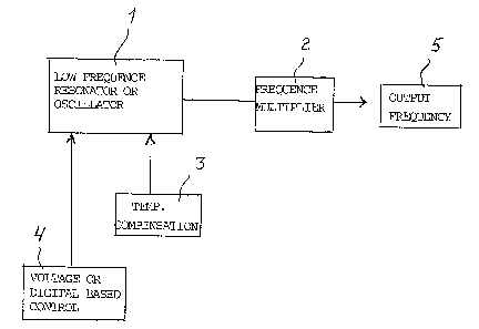
A method to control a frequency oscillator, as a crystal oscillator, and to
form an oscillating circuit in order to produce a frequency oscillator
improved to its qualities, in which the frequency of reference oscillator (1)
is changed by means of frequency multiplier (2) into output frequency. As
frequency oscillator a low frequency oscillator (1) is used, the control of
which output frequency (5) is carried out adjusting the low frequency
oscillator (1) by means of control arrangement (4).
L'invention concerne un procédé permettant de commander un oscillateur, tel qu'un oscillateur à cristal, et de former un circuit d'oscillation afin de produire un oscillateur à qualités améliorées. La fréquence d'un oscillateur de référence (1) est modifiée au moyen d'un multiplicateur de fréquence (2) dans une fréquence de sortie. On utilise un oscillateur basse fréquence comme oscillateur, la commande de fréquence de sortie (5) effectuant un réglage de l'oscillateur basse fréquence (1) au moyen d'un agencement de commande (4).
Note: Claims are shown in the official language in which they were submitted.
Note: Descriptions are shown in the official language in which they were submitted.
2024-08-01:As part of the Next Generation Patents (NGP) transition, the Canadian Patents Database (CPD) now contains a more detailed Event History, which replicates the Event Log of our new back-office solution.
Please note that "Inactive:" events refers to events no longer in use in our new back-office solution.
For a clearer understanding of the status of the application/patent presented on this page, the site Disclaimer , as well as the definitions for Patent , Event History , Maintenance Fee and Payment History should be consulted.
| Description | Date |
|---|---|
| Time Limit for Reversal Expired | 2010-09-07 |
| Application Not Reinstated by Deadline | 2010-09-07 |
| Deemed Abandoned - Failure to Respond to Maintenance Fee Notice | 2009-09-08 |
| Letter Sent | 2008-10-29 |
| Request for Examination Received | 2008-09-04 |
| Request for Examination Requirements Determined Compliant | 2008-09-04 |
| All Requirements for Examination Determined Compliant | 2008-09-04 |
| Letter Sent | 2007-08-08 |
| Inactive: Delete abandonment | 2007-08-08 |
| Letter Sent | 2007-08-08 |
| Letter Sent | 2007-08-08 |
| Letter Sent | 2007-08-08 |
| Inactive: Abandoned - No reply to Office letter | 2007-06-07 |
| Inactive: Single transfer | 2007-06-06 |
| Inactive: Courtesy letter - Evidence | 2006-05-16 |
| Inactive: Cover page published | 2006-05-12 |
| Inactive: Notice - National entry - No RFE | 2006-05-09 |
| Application Received - PCT | 2006-03-28 |
| National Entry Requirements Determined Compliant | 2006-03-06 |
| National Entry Requirements Determined Compliant | 2006-03-06 |
| Application Published (Open to Public Inspection) | 2005-03-17 |
| Abandonment Date | Reason | Reinstatement Date |
|---|---|---|
| 2009-09-08 |
The last payment was received on 2008-09-04
Note : If the full payment has not been received on or before the date indicated, a further fee may be required which may be one of the following
Patent fees are adjusted on the 1st of January every year. The amounts above are the current amounts if received by December 31 of the current year.
Please refer to the CIPO
Patent Fees
web page to see all current fee amounts.
| Fee Type | Anniversary Year | Due Date | Paid Date |
|---|---|---|---|
| MF (application, 3rd anniv.) - standard | 03 | 2006-09-05 | 2006-03-06 |
| MF (application, 2nd anniv.) - standard | 02 | 2005-09-06 | 2006-03-06 |
| Basic national fee - standard | 2006-03-06 | ||
| Registration of a document | 2007-06-06 | ||
| MF (application, 4th anniv.) - standard | 04 | 2007-09-05 | 2007-09-04 |
| MF (application, 5th anniv.) - standard | 05 | 2008-09-05 | 2008-09-04 |
| Request for examination - standard | 2008-09-04 |
Note: Records showing the ownership history in alphabetical order.
| Current Owners on Record |
|---|
| ZIPIC OY |
| Past Owners on Record |
|---|
| KLAUS TURHANEN |
| RAIMO ANTERO MAEKELAE |
| SAMPO SAKARI AALLOS |

