Note: Descriptions are shown in the official language in which they were submitted.
CA 02538113 2006-03-08
WO 2005/029329 PCT/US2004/030127
A SYSTEM AND METHOD FOR TESTING AND CONFIGURING
SEMICONDUCTOR FUNCTIONAL CIRCUITS
RELATED APPLICATIONS
[0001] This application claims the benefits of co-pending~commonly-owned LJ.S.
Patent Application Serial No. 60/503,710, filed September 15, 2003,~U.S.
Patent
Application Serial No. 10/740,721, filed December 18, 2003, U.S. Patent
Application
Serial No. 10/740,722, filed December 18, 2003, U.S. Patent Application Serial
No.
10/740,723, filed December 18, 2003, U.S. Patent Application Serial No.
10/740,779,
filed December 18, 2003, and U..S: Patent ApplicatioriySerial No. 10/876,340,
filed June
23, 2004, which are hereby incorporated by this reference.
FIELD
[0002] The present invention relates to the field of semiconductor
manufacturing.
In particular, the present invention relates to a system and method for
dynamically
configuring operational characteristics of functional components within an
integrated
circuit.
BACKGROUND
[0003] Electronic systems and circuits have made a significant contribution
towards the advancement of modern society and are utilized in a number of
applications
CA 02538113 2006-03-08
WO 2005/029329 PCT/US2004/030127
to achieve advantageous results. Numerous electronic technologies such as
digital
computers, calculators, audio devices, video equipment, and telephone systems
have
facilitated increased productivity and reduced costs in analyzing and
communicating data
in most areas of business, science, education and entertainment. Electronic
systems
providing these advantageous results often include integrated circuits. It is
desirable to
utilize integrated circuits with very high reliability characteristics to
prevent erroneous
results. However, designing and building integrated circuits with diverse
functionality
and performance characteristics is challenging. Additionally, the
manufacturing process
to build the integrated circuits is highly complex and resource intensive.
[0004] Manufacturing integrated circuits is an expensive, resource intensive
activity, in which numerous computational components are included in a single
integrated
circuit unit. The computational components are usually required to be capable
of
performing a variety of tasks with very high reliability. Various applications
often
require different performance levels and functionality. Traditionally, each
die is
fabricated with a predetermined quantity of properly performing components
providing
set functionality. However, providing appropriate and efficient functionality
at
acceptable reliability is often difficult. For example, many traditional
approaches require
that there be few or no defective components included in the integrated
circuit.
[0005] Conventionally, integrated circuits are manufactured in wafers
comprising
a number of die, with each die comprising an integrated circuit having
numerous
functional components. The number of die that are functionally acceptable from
a given
2
CA 02538113 2006-03-08
WO 2005/029329 PCT/US2004/030127
wafer is referred to as the yield from the wafer. It is desirable to maintain
relatively high
yields in order to eliminate waste, save cost and speed-up the effective
manufacturing
time for a given number of die. Yields for wafers with high performance die
with a large
number of components can be very low.
[0006] One method used by memory chip makers for mitigating the impact of the
occurrence of defective components within an integrated circuit die is to
produce the die
with more components, e.g. memory cells, than required. If there is a
defective
component the defective component is disconnected 'and one of the "surplus"
components
is utilized. This approach usually results in considerable waste of precious
die area and
resources on fabricating components that remain "surplus" even after replacing
defective
components. Such surplus components do not contribute to functionality and/or
operational productivity. A significant number of die end up having numerous
"surplus"
components with perfectly good operational capabilities that are not utilized.
[0007] Another traditional attempt at addressing defective components is to
remove functional capability if one functional component associated with a
particular
function is defective. For example, if a floating point acceleration component
of a
processor is defective, the floating point acceleration functionality is
removed or disabled
using conventional repair techniques, and the processor becomes a non-floating
point
acceleration processor. In addition, the end result is a usable integrated
circuit with
limited capability and that does not provide a full range of functionality
(e.g., not able to
perform floating point operations).
3
CA 02538113 2006-03-08
WO 2005/029329 PCT/US2004/030127
SUMMARY
[0008] The present invention systems and methods enable configuration of
functional components in integrated circuits. A present invention system and
method can
flexibly change the operational characteristics of functional components in an
integrated
circuit die based upon a variety of factors including manufacturing defects,
compatibility
characteristics, performance requirements, and system health (e.g., the number
of
components operating properly). In one embodiment of the present invention,
functional
component operational behavior is analyzed. The analysis can be performed at
various
levels of configuration abstraction and component organization (e.g.,
topological
inversion analysis) and can be performed in parallel for a plurality of
functional
components. Operational characteristic settings are determined based upon
results of the
analysis. In one embodiment, the operational characteristics settings are
determined at
various levels of configuration abstraction and component organization. A
functional
component reconfiguration process is performed in accordance with the
operational
characteristic settings. In one exemplary implementation, the functional
component
reconfiguration process includes determining if an indicated functional
component
configuration alteration is valid; directing alteration of the functional
component
configuration; and diverting workflow in accordance with the alteration of the
functional
component configuration.
[0009] Functional component configuration related information can be presented
in a variety of convenient formats including a graphical user interface (GUI).
In one
4
CA 02538113 2006-03-08
WO 2005/029329 PCT/US2004/030127
embodiment, the GUI indicates a pass or fail status for functional component
building
blocks at various levels of granularity and in real time. The graphical user
interface can
present topological inversion information in a user friendly manner that are
otherwise
dispersed in an imperfect Cartesian order. The graphical user interface can
also facilitate
user interaction with various functional component operational behavior
analyzing
features and operational characteristics settings determining features. For
example, the
graphical user interface can facilitate user interaction in failing pattern
recognition,
production test tuning and field configuration algorithm adjustment.
[0011] In one embodiment, a present invention configuration system includes
functional components, a distribution component, a functional component
configuration
controller and optionally a collection component. The functional components
perform
processing operations (e.g., graphics processing operations, floating point
operations,
etc.). The distribution component distributes workflow information (e.g.,
graphics
processing information, floating point processing information, etc.) to the
functional
components. The fixnctional component configuration controller configures
operational
characteristics of the functional components. The collection component
"collects" the
output or results from the functional components and aggregates the results of
the
operations for use in achieving a common objective.
[0011 ] In one exemplary implementation, the changes to operational
characteristics of a functional component are coordinated with changes to
other
functional components. Workflow scheduling and distribution is also adjusted
based
CA 02538113 2006-03-08
WO 2005/029329 PCT/US2004/030127
upon the changes to the operational characteristics of the functional
components. For
example, the functional component configuration controller changes the
operational
characteristics settings and provides an indication of the changes to a
workflow
distribution component. The workflow distribution component changes the
workflow
schedule based upon the operational characteristics settings. For example, the
work flow
is diverted to or away from particular functional components.
[0012] The present invention system and method can be utilized in a variety
testing operations. A chip is tested (e.g., in accordance with a built in self
test) and
defective functional components of the chip are identified. The testing can be
performed
in parallel and at probe or final sort. Performing the testing in parallel
provides cost
savings and faster results. The present invention built in self repair (BISR)
features of
disabling defective components and enabling replacement components provides a
number
of flexible features. For example, enable integrated circuit chips with
defective
functional components to be salvaged and facilitate increased wafer yield in
integrated
circuit manufacturing in one embodiment. Traditionally, the integrated
circuits with the
defective functional components would otherwise be discarded resulting in the
costs of
producing a wafer being assigned to fewer acceptable die. In one embodiment, a
present
invention system and method disables defective functional components in the
die in a
manner that maintains the basic functionality of the chip.
[0013] In one embodiment, centralized resources are utilized in the
configuration
of remote integrated circuits. A remote functional component configuration
architecture
facilitates configuration of functional components included in a remotely
located
6
CA 02538113 2006-03-08
WO 2005/029329 PCT/US2004/030127
integrated circuit die. In one exemplary implementation a die functional
component
reconfiguration request process is engaged in wherein a system requests a
reconfiguration
code from a remote resource. The code request includes a reconfiguration code
permission indicator that indicates the requester is authorized to receive a
reconfiguration
code (e.g., the requester has made a requisite payment, has an authorized
system, etc.). A
reconfiguration code production process is executed in which a request for a
reconfiguration code and a permission indicator are received, validity of the
permission
indicator is analyzed, and a reconfiguration code is provided. A die
functional
component reconfiguration process is performed on the die when an appropriate
reconfiguration code is received by the die.
7
CA 02538113 2006-03-08
WO 2005/029329 PCT/US2004/030127
DESCRIPTION OF THE DRAWINGS
[0014] The accompanying drawings, which are incorporated in and form a part of
this specification, illustrate embodiments of the invention by way of example
and not by
way of limitation. The drawings referred to in this specification should be
understood as
riot being drawn to scale except if specifically noted.
[0015] Figure lA is a block diagram of an integrated circuit in accordance
with
one embodiment of the present invention.
[0016] Figure 1B is a block diagram of an integrated circuit having functional
components organized in pipelines in accordance with one embodiment of the
present
invention.
[0017] Figure 1 C is a block diagram of a multiprocessor integrated circuit in
accordance with one embodiment of the present invention.
[0018] Figure 1D is a block diagram of an exemplary mask array implementation
in accordance with one embodiment of the present invention to control
different
objectives.
[0019] Figure 2 is a block diagram of a computer system in which embodiments
of the present invention can be implemented.
8
CA 02538113 2006-03-08
WO 2005/029329 PCT/US2004/030127
[0020] Figure 3 is a block diagram of a graphics pipeline in accordance with
one
embodiment of the present invention.
[0021] Figure 4 is a flow chart of a functional component configuration method
in
accordance with one embodiment of the present invention.
[0022] Figure 5 is a flow chart of a reduced performance circuit salvage
method
in accordance with one embodiment of the present invention.
[0023] Figure 6 is a block diagram of a testing environment in accordance with
one embodiment of the present invention.
[0024] Figure 7 is a flow chart of a die classification process in accordance
with
one embodiment of the present invention.
[0025] Figure 8 is a block diagram of a processing unit in accordance with one
embodiment of the present invention.
[0026] Figure 9 is a flow chart of a wafer yield optimization method in
accordance with one embodiment of the present invention.
9
CA 02538113 2006-03-08
WO 2005/029329 PCT/US2004/030127
[0027] Figure 10 is a block diagram of a functional component configuration
architecture in accordance with one embodiment of the present invention.
[0028] Figure 11 is a flow chart of a remote reconfiguration method in
accordance with one embodiment of the present invention.
[0029] Figure 12 is a block diagram of another exemplary functional component
configuration system in accordance with one embodiment of the present
invention.
[0030] Figure 13 is a flow chart of a functional component configuration
analysis
process in accordance with one embodiment of the present invention.
[0031 ] Figure 14 is a flow chart of a flexible integrated circuit testing
method in
accordance with one embodiment of the present invention.
[0032] Figure 15 is a block diagram of an integrated circuit analysis system
in
accordance with one embodiment of the present invention.
CA 02538113 2006-03-08
WO 2005/029329 PCT/US2004/030127
DETAILED DESCRIPTION
[0033] Reference will now be made in detail to the preferred embodiments of
the
invention, examples of which are illustrated in the accompanying drawings.
While the
invention will be described in conjunction with the preferred embodiments, it
will be
understood that they are not intended to limit the invention to these
embodiments. On the
contrary, the invention is intended to cover alternatives, modifications and
equivalents,
which may be included within the spirit and scope of the invention as defined
by the
appended claims. Furthermore, in the following detailed description of the
present
invention, numerous specific details are set forth in order to provide a
thorough
understanding of the present invention. However, it will be obvious to one of
ordinary
skill in the art that the present invention may be practiced without these
specific details.
In other instances, well known methods, procedures, components, and circuits
have not
been described in detail as not to unnecessarily obscure aspects of the
present invention.
[0034] Some portions of the detailed descriptions which follow are presented
in
terms of procedures, logic blocks, processing, and other symbolic
representations of
operations on data bits within a computer memory. These descriptions and
representations are the means generally used by those skilled in data
processing arts to
effectively convey the substance of their work to others skilled in the art. A
procedure,
logic block, process, etc., is here, and generally, conceived to be a self
consistent
sequence of steps or instructions leading to a desired result. The steps
include physical
manipulations of physical quantities. Usually, though not necessarily, these
quantities
11
CA 02538113 2006-03-08
WO 2005/029329 PCT/US2004/030127
take the form of electrical, magnetic, optical, or quantum signals capable of
being stored,
transferred, combined, compared, and otherwise manipulated in a computer
system. It
has proven convenient at times, principally for reasons of common usage, to
refer to these
signals as bits, values, elements, symbols, characters, terms, numbers, or the
like.
[0035] It should be borne in mind, however, that all of these and similar
terms are
associated with the appropriate physical quantities and are merely convenient
labels
applied to these quantities. Unless specifically stated otherwise as apparent
from the
following discussions, it is appreciated that throughout the present
application,
discussions utilizing terms such as "processing", "computing", "calculating",
"determining", "displaying" or the like, refer to the action and processes of
a computer
system, or similar processing device (e.g., an electrical, optical, or
quantum, computing
device) , that manipulates and transforms data represented as physical (e.g.,
electronic)
quantities. The terms refer to actions and processes of the processing devices
that
manipulate or transform physical quantities within a computer system's
component (e.g.,
registers, memories, other such information storage, transmission or display
devices, etc.)
into other data similarly represented as physical quantities within other
components.
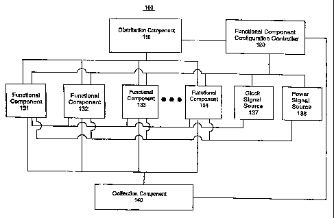
[0036] Figure lA is a block diagram of integrated circuit 100 in accordance
with
one embodiment of the present invention. Integrated circuit 100 comprises
distribution
component 110, functional component configuration controller 120, collection
component 140 and functional components 131, 132, 133 and 134. Distribution
component 110 is coupled to functional components 131, 132, 133 and 134, which
are
12
CA 02538113 2006-03-08
WO 2005/029329 PCT/US2004/030127
coupled to collection component 140. Functional component configuration
controller
120 is coupled to distribution component 110, functional components 131, 132,
133 and
134, and collection component 140. In one embodiment of the present invention,
the
components of integrated circuit 100 are included in a single die. The
components of
integrated circuit 100 cooperatively operate to perform information processing
(e.g., data
manipulation). In one exemplary implementation, the components of integrated
circuit
100 perform information processing related to a common objective (e.g.,
graphics
pipeline processing associated with producing an image).
[0037] Distribution component 110 selectively distributes information to
functional components 131 - 134 (e.g., enabled functional components). It is
appreciated
that distribution component 110 can distribute a variety of information. For
example,
distribution component 110 can distribute workflow information. The workflow
information can be information or data for processing in association with a
common
objective. For example, the workflow information can be graphics related
information
(e.g., a single stream of information in which various parts of the
information stream
include pixel information for sequentially configured pixels of an image). In
one
exemplary implementation, distribution component 110 receives a single stream
of
workflow information or data (e.g., graphics data) and distributes the
workflow
information to functional components 131-134. For example, the single stream
of
information can include information related to a first pixel, a second pixel,
and a third
pixel. Distribution component 110 receives the single stream of pixel
information (e.g.,
a sequence of packets) and distributes the information (e.g., as individual
packets) related
13
CA 02538113 2006-03-08
WO 2005/029329 PCT/US2004/030127
to the first pixel to functional component 13 l, the information related to
the second pixel
to functional component 132 and the information related to the third pixel to
functional
component 133. In another exemplary implementation, the distribution component
110
receives a single stream of information related to floating point calculations
and
distributes information associated with a first floating point calculation to
functional
component 131, information associated with a second floating point calculation
to
functional component 132, and information associated with a third floating
point
calculation to functional component 133. In one embodiment, distribution
component
110 can also receive multiple information streams and distribute the
information to the
functional components 131-134. It is appreciated that distribution component
110 can
be implemented in a variety of embodiments, including embodiments in which
distribution component 110 provides functions or performs tasks in addition to
distributing the workflow information.
[0038] Functional components 131 - 134 can include a variety of
implementations
in which the functional components 131-134 perform different functional
operations or
tasks. In one embodiment functional components 131 - 134 provide similar
functionality
(e.g., perform parallel operations). For example, in one embodiment functional
components 131-134 can perform graphics processing related tasks (e.g.,
shading,
texturing, occlusion culling, etc). In another embodiment, functional
components 131-
134 can perform floating point related processing.
14
CA 02538113 2006-03-08
WO 2005/029329 PCT/US2004/030127
[0039] Collection component 140 "collects" the output or results from
functional
components 131-134. In one embodiment, collection component 140 concatenates
or
aggregates the results of the operations for use in achieving the common obj
ective. For
example, the collection component 140 can aggregate the results for
communication to a
graphics 'buffer. In another embodiment, the collection component 140 is a
graphics
buffer. In yet another embodiment, collection component 140 can aggregate the
results
of floating point calculations.
[0040] The components of integrated circuit 100 also cooperatively operate to
flexibly configure functional component operational characteristics (e.g.,
enable/disable a
functional component, change clock speed, change operating voltage, etc.).
Functional
component configuration controller 120 controls adjustments in operational
characteristics (e.g., disable/enable, etc.) of one or more of the functional
components
131 - 134 and can provide information to distribution component 110 and
collection
component 140 regarding the adjustment. For example, functional component
configuration controller 120 can disable or enable a functional component
(e.g., disable
or enable functional component 132). Functional component configuration
controller
120 can notify distribution component 110 of the change to functional
component 132
operating characteristics (e.g., which of the functional components is
enabled, disabled,
etc.).
[0041] Distribution component 110 can use information about the operational
characteristics of functional component 132 in distributing workflow
information. In one
CA 02538113 2006-03-08
WO 2005/029329 PCT/US2004/030127
embodiment, the distribution component 110 can factor the configuration of the
functional components into distribution of information (e.g., workflow
including data for
processing) to the functional components. If one of the processor functional
components
is disabled (e.g., because it is defective), distribution component 110
distributes the
information to the other remaining processor functional components to handle
the "work
flow". For example, if functional component 132 is disabled by functional
component
configuration controller 120, distribution component 110 is notified that
functional
component 132 is disabled and distribution component 110 can route workflow to
other.
functional components (e.g., 131, 133, and/or 134). If functional component
132 is
enabled by functional component configuration controller 120, distribution
component
110 is notified that functional component 132 is enabled and distribution
component 110
can route workflow to functional component 132. Distribution component 110 can
also
distribute the information to remaining enabled functional components based
upon the
performance configuration (e.g., clock speed) of the functional components. In
one
exemplary implementation, tasks with greater performance demands (e.g.,
critical tasks)
are routed to functional components with greater performance characteristics
or
capabilities (e.g., faster). For example, three dimensional (3D) graphics
information can
be routed to a high performance (e.g., high speed) graphics pipeline and two
dimensional
(2D) graphics information can be routed to a lower performance (e.g., slower
speed)
graphics pipeline. In one embodiment the information is distributed in
accordance with
scoreboarding algorithms.
16
CA 02538113 2006-03-08
WO 2005/029329 PCT/US2004/030127
[0042] In one embodiment of the present invention, functional component
configuration controller 120 directs changes to operational characteristics of
functional
components 131 - 134. The operational characteristics can impact the
performance of
functional components 131 - 134. For example, functional component
configuration
controller 120 can change an operational characteristic state of functional
components
131 - 134 (e.g., enable or disable the functional component). In one exemplary
implementation, functional component configuration controller 120 can alter
the speed at
which a functional component operates (e.g., by changing a clock frequency)
and/or the
power consumed by a functional component (e.g., by changing the voltage
supplied to the
functional component). For example, functional component configuration
controller 120
can direct clock source 137 to change a frequency of a clock signal supplied
to functional
components 131-134 and/or power supply 138 to change the voltage of a power
signal
supplied to functional components 131 - 134.
[0043] It is appreciated that the present invention is readily adaptable for
utilization with a variety of functional components. Functional components 131
-134 can
be functional units that provide a variety of different functions (e.g.,
floating point, pixel
shading, vertex shading, storage, buffering, etc.). In one exemplary
implementation, the
functional components can perform similar operations at substantially the same
time
(e.g., concurrently in parallel). In one embodiment of the present invention,
the
functional components are active functional components. The functional
components
can also include a number of components organized in a core and/or sub cores
(e.g.,
building blocks associated with a particular function). In one embodiment of
the present
17
CA 02538113 2006-03-08
WO 2005/029329 PCT/US2004/030127
invention, cores or sub-cores can be tested and/or reconfigured individually.
For
example, a particular core can be enabled and/or disabled in accordance with
present
invention reconfiguration features.
[0044] In one embodiment, the functional components are processor components
~e.g., floating point components, pixel shader components, vertex processor
components,
etc.) included in a processing unit. It is appreciated that the present
invention can be
readily implemented in a variety of processing units, including a central
processing unit
(CPU), a graphics processing unit (GPU), andlor an embedded processing unit.
In one
exemplary implementation, the processing unit includes a scoreboarding
algorithm for
allocating tasks to the processor functional components (e.g., floating point
components).
As results are processed by the processor functional components the scoreboard
tracks
which operand is required by a processor functional component and schedules
it. The
results from the individual processor functional components can be combined to
provide
an overall result. The scoreboard can factor a functional component
configuration into
the scheduling of tasks. For example, if one of the processor functional
components is
disabled (e.g., because it is defective), the scoreboard reschedules the other
remaining
processor functional components to handle the processing work flow.
[0045] The present invention can be implemented in a pipeline type (e.g., a
vector
type, thread type, etc.) processing environment. Figure 1 B is a block diagram
of pipeline
integrated circuit 150 in accordance with one embodiment of the present
invention.
Pipeline integrated circuit 150 is an implementation of integrated circuit 100
in which the
18
CA 02538113 2006-03-08
WO 2005/029329 PCT/US2004/030127
functional components are pipelines. Integrated circuit 150 comprises
distribution
component 151, functional component configuration controller 152, collection
component 154 and pipelines 171, 172, 173 and 174. Pipelines 171, 172, 173 and
174
perform pipeline operations (e.g., fetch, decode and execute instructions).
Functional
component configuration controller 152 controls the operational
characteristics of
pipelines 171 through 174 and also provides information to distribution
component 151
and collection component 154 regarding operational characteristics of
pipelines 171
through 174 (e.g., information regarding which of the functional components is
disabled
and/or enabled). The control of operational characteristics can be performed
at varying
granularity. For example, a pipeline can include multiple individual
functional
components (not shown) within each pipeline which can also be configured
(e.g.,
enabled, disabled, etc.) on an individual functional component basis.
[0046 The components of pipeline integrated circuit 150 operate similar to the
components of integrated circuit 100. For example, workflow information is
diverted or
routed in a similar manner. Functional component configuration controller 152
provides
information to distribution component 151 regarding the operational
characteristics of the
functional components 171-174 (e.g., disabled, enabled, speed, voltage, etc).
Distribution component 151 distributes information to the pipelines 171-174
based. in
part upon the operation characteristic information (e.g., distributes workflow
information
to enabled functional components and not disabled functional components).
Collection
component 140 "collects" (e.g., concatenates or aggregates) the output of
pipelines 171-
174 (e.g., concatenates or aggregates the results for storage in a graphics
buffer). In one
19
CA 02538113 2006-03-08
WO 2005/029329 PCT/US2004/030127
embodiment, functional component configuration controller 152 can direct clock
source
175 to change a frequency of a clock signal supplied to functional components
171-174
and/or power supply 177 to change the voltage of a power signal supplied to
fiuzctional
components 171 - 174.
[0047] A present invention integrated circuit can be implemented at a variety
of
integration levels (e.g., a variety of die hierarchies and architectures).
Figure 1C is a
block diagram of multiprocessor integrated circuit 190, another embodiment of
a present
invention die hierarchy. The components of multiprocessor integrated circuit
190 are
similar to integrated circuit 100 except the functional components are
processors.
Multiprocessor integrated circuit 190 comprises distribution component 191,
functional
component configuration controller 192, collection component 194 and
processors 195,
197, 198 and 199. In one embodiment, processors 195, 197, 198 and 199 are
included in
a single die and coupled to a common cache memory. Functional component
configuration controller 192 can direct operational characteristics
adjustments (e.g.,
disables/enables) to one or more of the processors 195 - 199 and provides
operational
characteristic information to distribution component 191 and collection
component 194
indicating the operational characteristics of processors 195 -199 (e.g.,
indicates if a
processor is disabled/enabled). In one exemplary implementation, integrated
circuit 190
still provides complete functionality even if functional component
configuration
controller 192 disables a processor (e.g., 195, 197, 198, or 199).
CA 02538113 2006-03-08
WO 2005/029329 PCT/US2004/030127
[0048] The components of multiprocessor integrated circuit 190 operate similar
to
the components of integrated circuit 100. For example, workflow information is
diverted
or routed in a similar manner. Functional component configuration controller
192
provides information to distribution component 191 regarding operational
characteristics
of the functional components (e.g., disabled, enabled, speed, voltage, etc).
Distribution
component 191 distributes information (e.g., workflow data) to the processors
195 -199.
The distribution is based in part upon the operation characteristic
information (e.g.,
distributes workflow information to enabled functional components and not
disabled
functional components). In one exemplary implementation, collection component
194 is
a memory (e.g., a common cache) which "collects" or stores the output of
processors 195
- 199. In one embodiment, functional component configuration controller 192
can direct
clock source 181 to change a frequency of a clock signal supplied to
functional
components 195 -199 and/or power supply 182 to change the voltage of a power
signal
supplied to functional components 195 - 199.
[0049] A distinction is made between performance and functionality in one
embodiment of the present invention. In some instances, the present invention
does not
limit functionality when changing operational characteristics in the sense
that a particular
type of function or task is still capable of being performed even though the
function or
task may be accomplished at a different performance level. In one embodiment,
a
functional component configuration controller does not disable all the
functional
components capable of performing tasks in parallel. For example, if a die has
two
parallel floating point functional components in a processor and functional
component
21
CA 02538113 2006-03-08
WO 2005/029329 PCT/US2004/030127
configuration alters the enablement characteristic or state (e.g., disables)
one of the
floating point functional components, the work flow is "rerouted" to the
remaining
enabled floating point functional components. The performance level of
floating point
activities may change (e.g., slow down) since the work flow is being handled
by one
floating point functional component instead of two. However, the die still has
the ability
to provide the same functionality or task (e.g., perform the floating point
functions).
[0050] In one embodiment of the present invention, integrated circuits (e.g.,
integrated circuit 100, integrated circuit 150, integrated circuit 190, etc.)
are marked with
a performance indicator that corresponds to the performance capabilities
(e.g., the
number of functional components that are enabled and/or disabled). The marking
can be
an electronically readable marking and/or an ink marking (e.g., on a die). The
marking
can be an indicator of the quality rating of the integrated circuit. The
marking can also
coiTespond to a performance metric associated with the integrated circuit
(e.g., a
processing speed, bandwidth, etc.).
[0051 ] It is appreciated that the functional component configuration
controllers
120, 152, and/or 192 can direct functional component changes in accordance
with a
variety of objectives. For example, a functional component configuration
controller can
alter operational characteristics of functional components based upon yield
issues,
compatibility issues, performance issues, system "health" issues, etc. It is
also
appreciated that functional component configuration controllers 120, 152,
andlor 192 can
22
CA 02538113 2006-03-08
WO 2005/029329 PCT/US2004/030127
include a variety of implementations to achieve the objectives, including a
software
programmable register or mask, hardcoded mask, etc.
[0052] In one embodiment, a functional component configuration controller
(e.g.,
120, 152 and/or 192) directs changes in the operational characteristics of
functional
components to address yield issues. The present invention has the benefit of
facilitating
increased wafer yield in integrated circuit manufacturing. A present invention
system
and method enables integrated circuits with some defective functional
components to be
salvaged. Traditionally, die with defective functional components are
discarded resulting
in the costs of producing a wafer being assigned to fewer acceptable die. The
present
invention permits some die with defective functional units to be used to
perform the same
types of functions and thereby maintain functionality even though the
disablement of the
defective components may impact performance. Increasing the number of useful
die on a
wafer permits the cost of wafer production to be assigned to a greater number
of
acceptable die. By permitting the fixed cost of wafer production to be
assigned to a
greater number of die, the cost per die can decrease, even though the lower
performing
die may be sold at a lower price.
[0053] The present invention facilitates "salvaging" of die even though
some'of
the die may operate at different performance levels. In one exemplary
implementation,
the die that would otherwise be discarded are able to provide the same
functionality in the
sense that the die execute the same type of tasks. For example, a processor
with parallel
floating point functional components capable of performing floating point
operations is
23
CA 02538113 2006-03-08
WO 2005/029329 PCT/US2004/030127
still able to perform floating point ~i~erations since in biie embodiment the
present
invention does not disable all the parallel floating point components and
"reroutes"
workflow from the disabled parallel floating point components to the remaining
floating
point components. Die with more disabled components may perform the tasks at a
different level (e.g., slower) because some parallel components are disabled.
However,
the die still has the ability to provide the same functionality (e.g., perform
the same
tasks).
[0054] In one embodiment, a functional component configuration controller
(e.g.,
120, 152 andlor 192) directs operational characteristic changes (e.g., enable,
disable, etc.)
to functional components during manufacturing testing. For example, a
functional
component configuration controller (e.g., 120, 152 or 192) disables a
functional
component (e.g., 132, 173, or 198 respectively) if testing indicates the
functional
component is defective and enables a functional component (e.g., 131, 174, 197
respectively) if testing indicates the functional component is not defective.
[0055] In one embodiment of the present invention, a functional component
configuration controller (e.g., 120, 152 and/or 192) directs changes in the
operational
characteristics of functional components to address "self health" issues. In
one
exemplary implementation, the functional component controller addresses self
health
issues in the "field" or after initial shipment from the manufacturer. In one
exemplary
implementation, an integrated circuit is capable of running in the field "self
health" tests.
For example, if a "self health" test results in an indication of a defective
functional
24
CA 02538113 2006-03-08
WO 2005/029329 PCT/US2004/030127
component, a functional component configu~atiori controller (e.g., 120, 152
and/or 192)
disables the defective functional component arid provides an indication that
the functional
component is disabled to a distribution component (e.g., 110, 150, or 191). In
one
embodiment of the present invention, the self health test is compliant with
International
Electrical and Electronic Engineering (IEEE) Standard 1149.1 (also referred to
as Joint
Task Action Group (JTAG) testing). In an alternate embodiment, the self health
test is a
proprietary test for checking the operational integrity of the system. In yet
another
embodiment, a functional component is enabled if a "self health" test in the
field
indicates the functional component is not defective.
[0056] In yet another embodiment, if a non-enabled non-defective functional
component that performs similar types of tasks or functions as a defective
functional
component is available, the non-enabled non defective functional component is
enabled if
the defective component is disabled. For example, integrated circuit 100 of
figure 1 can
be initially shipped with functional components 131 and 132 enabled and
functional
components 133 and 134 disabled even through they are non defective (e.g., for
market
segmentation reasons, etc.). If a field self health test later indicates that
functional
component 132 becomes defective, functional component controller' 120 can
disable
functional component 132 and enable functional component 133 and work flow
that
would have flowed to functional component 132 if it was not disabled is
distributed (e.g.,
by distribution component 110) to functional component 133. Thus, disabling
functional
component 132 in effect removes the problems associated with defects in
functional
component 132, while enabling previously disabled functional component 133
permits
CA 02538113 2006-03-08
WO 2005/029329 PCT/US2004/030127
the same type of functionality or tasks to be performed on the workflow at the
same
performance level and thereby the system is effectively "self healing".
[0057] In one embodiment of the present invention, a functional component
configuration controller (e.g., 120, 152 and/or 192) directs changes in the
operational
characteristics of functional components to address compatibility issues. In
one
embodiment, a functional component controller included in a graphics
accelerator is
capable of recognizing chipsets that are compatible with features of the
graphics
accelerator and changes operational characteristics of the graphics
accelerator
accordingly. For example, if the functional component configuration controller
is
controlling operational characteristics of graphics pipelines, the functional
component
configuration controller can enable a higher number of graphics pipelines if
the chip set
supports it and is compatible with the utilization of a higher number of
graphics
pipelines. For example, a graphics accelerator and a chip set are manufactured
by the
same manufacturer and the functional component controller included in the
graphics
accelerator can receive a signal identifying a chip set included in the same
system as the
graphics accelerator. In one embodiment of the present invention,
compatibility is
established by a driver and a functional component controller directs changes
to the
operational characteristics of the fiuzctional components accordingly.
[0058] In one embodiment of the present invention, a functional component
configuration controller (e.g., 120, 152 and/or 192) directs changes in
the.operational
characteristics of functional components to address performance issues. In one
26
CA 02538113 2006-03-08
WO 2005/029329 PCT/US2004/030127
embodiment, performance mask 40 provides an indication of operational
characteristics
for functional components based upon performance issues. For example, a
particular
application is being run and desirable supported functional component
operational
characteristics are enabled. If the application is a graphics application
additional graphics
pipelines can be enabled and/or the clock speed of existing graphics
application pipelines
can be increased. In one embodiment of the present invention, the type of the
system can
be factored into performance operational changes, for example in mobile
devices the
performance can be adjusted to conserve power.
[0059] It is appreciated that there are a variety of functional component
configuration controller embodiments for implementing functional component
changes in
accordance with different objectives. Figure 1D is a block diagram ofmask
array 10
utilized by a functional component controller in accordance with one
embodiment of the
present invention to control different objectives. Each mask in the mask array
can
correspond to a particular operational obj ective. In one exemplary
implementation, mask
array 10 comprises yield mask 20, compatibility mask 30, performance mask 40,
and self
healing mask 50. In one exemplary implementation, each column 11 through 18 is
associated with one of eight functional components. Each cell (e.g., cell 99)
includes an
operational characteristic setting value. For example, an operational
characteristic setting
value of logical one can correspond to enabling the functional component, a
high clock
speed for the component, a high voltage level for the component, etc.
Conversely an
operational characteristic setting value of logical zero can correspond to
disabling the
functional component, a low clock speed for the component, a low voltage level
for the
27
CA 02538113 2006-03-08
WO 2005/029329 PCT/US2004/030127
component, etc. It is appreciated that the present invention is readily
adaptable for
operational characteristic setting values that have varying increments of
granularity (e.g.,
very high speed, high speed, medium speed, low speed, very low speed). In one
exemplary implementation, mask array 10 is implemented in a register array.
[0060] Priorities can be assigned to the different objectives or masks. For
example, yield mask 20 can be assigned a higher priority than performance mask
40. In
this example, the operational characteristic setting value in cell 98 controls
over the
operational characteristic setting value in cell 97. If the setting value in
cell 98 indicates
that the functional component associated with column 12 is disabled, the
functional
component is disabled regardless of the setting value in cell 97. The values
in mask array
can also be utilized in a variety of algorithms that account for a variety of
considerations in determining an operational characteristic setting that is
implemented by
a functional component configuration controller. '
[0061] Yield mask 20 provides an indication of functional components that are
disabled due to yield issues (e.g., defects). For example, yield mask 20
includes
operational characteristic setting values that cause functional components to
be disabled
if the functional components have a manufacturing defect. In one exemplary
implementation, a functional component is permitted to be disabled if there is
another
operational functional component that can handle the work flow.
28
CA 02538113 2006-03-08
WO 2005/029329 PCT/US2004/030127
[0062] Compatibility mask 30 provides an indication of operational
characteristics for functional, components based upon compatibility issues.
For example,
a particular processor and chip set can exchange identification with one
another and
based upon the exchange of identification, compatible supported functional
component
operational characteristics can be enabled. In one embodiment of the present
invention,
compatibility is established by a driver and a corresponding operational
characteristic
setting value is entered in compatibility mask 30.
[0063] Performance mask 40 provides an indication of operational
characteristics
for functional components based upon performance issues. For example, a
particular
application is being run and a value is entered into performance mask 40
enabling
corresponding desirable supported functional component operational
characteristics. If
the application is a graphics application additional graphics pipelines can be
enabled
and/or the clock speed of existing graphics application pipelines can
increase. In one
embodiment of the present invention, the type of the system can be factored
into
performance operational changes, for example in mobile devices a value entered
in
performance mask 40 can direct a performance adjustment to conserve power. For
example, direct changes to operational characteristics of functional
components,
including disabling/enabling functional components, adjusting speed, voltage,
etc.).
[0064] Self healing mask 50 provides an indication of operational
characteristics
for functional components based upon field testing issues. For example,
results from
testing operations are utilized to determine changes in operational
characteristics for
29
CA 02538113 2006-03-08
WO 2005/029329 PCT/US2004/030127
functional components. In one exemplary implementation, a field test indicates
that an
enabled first functional component is defective. The operational
characteristic setting
value in the self healing mask cell associated with the first functional
component is
changed to indicate the first functional component is disabled and the
operational
characteristic setting value in the self healing mask cell associated with a
second
functional component that is disabled is changed to indicate the second
functional
component is enabled. By changing the respective operational characteristic
setting
values of the first and second functional components the defective first
component is
disabled and prevented from producing more problems and enabling a disabled
second
functional component allows the second functional component to perform the
workflow
that would otherwise be routed to the first functional component and thus the
system in
effect heals itself in that the same work flow is still able to be performed
without defects.
[0065] Figure 2 is a block diagram of a computer system 200, one embodiment of
a computer system upon which embodiments of the present invention can be
implemented. Computer system 200 includes central processor unit 201, main
memory
202 (e.g., random access memory), chip set 203 with north bridge 209 and south
bridge
205, removable data storage device 204, input device 207, signal
communications port
208, and graphics subsystem 210 which is coupled to display 220. Computer
system 200
includes several busses for communicatively coupling the components of
computer
system 200. Comruunication bus 291 (e.g., a front side bus) couples north
bridge 209 of
chipset 203 to central processor unit 201. Communication bus 292 (e.g., a main
memory
bus) couples north bridge 209 of chipset 203 to main memory 202. Communication
bus
CA 02538113 2006-03-08
WO 2005/029329 PCT/US2004/030127
292 (e.g., the Advanced Graphics Port interface) couples north bridge of
chipset 203 to
graphic subsystem 210. Communication buses 294 - 297 (e.g., a PCI bus) couple
south
bridge 205 of chip set 203 to removable data storage device 204, input device
207, signal
communications port 208 respectively. Graphics subsystem 210 includes graphics
processor 211 and graphics buffer 215.
[0066] The components of computer system 200 cooperatively operate to provide
versatile functionality and performance. The operating characteristics of
functional
components included in computer system 200 can change dynamically. In one
exemplary implementation, the components of computer system 200 cooperatively
operate to provide predetermined types of functionality, even though some of
the
functional components included in computer system 200 may be defective.
Communications bus 291, 292, 293, 294, 295 and 297 communicate information.
Central
processor 201 processes information. Main memory 202 stores information and
instructions for the central processor 201. Removable data storage device 204
also stores
information and instructions (e.g., functioning as a large information
reservoir). Input
device 206 provides a mechanism for inputting information and/or for pointing
to or
highlighting information on display 220. Signal communication port 208
provides a
communication interface to exterior devices (e.g., an interface with a
network). Display
device 220 displays information in accordance with data stored in frame buffer
215.
Graphics processor 211 processes graphics commands from central processor 201
and
provides the resulting data to graphics buffers 215 for storage and retrieval
by display
monitor 220.
31
CA 02538113 2006-03-08
WO 2005/029329 PCT/US2004/030127
[0067] The operational configurations of the functional components included in
computer system 200 are flexibly adaptable to meet a variety of objectives.
For example,
operational configurations of the functional components included in computer
system 200
are configurable to maintain execution of a type of function even if some of
the
functional components are disabled. In one exemplary implementation, central
processor
201 and graphics processor 211 are still capable of executing the same type of
processing
functions and main memory 202 stores information even through some of the
functional
components (e.g., floating point component, pixel shader component, memory
cell
component, etc) are disabled. In one embodiment, the processors include a
plurality of
functional components for performing processing operations. The operational
characteristics of the functional components can be altered. In one
embodiment, the
processors include a plurality of functional components for performing
processing
operations, wherein defective functional components included in the plurality
of
functional components are disabled. The processors also include a workflow
control
component for dispensing workflow to enabled processing components and
preventing
distribution of workflow to the disabled defective components. In one
exemplary
implementation, computer system 200 can continue to provide full functionality
even
through the functionality may be provided at a reduced performance level
(e.g., slower).
[0068] It is appreciated that the present invention can be implemented in a
variety
of embodiments. In one exemplary implementation the present invention can be
utilized
in processing systems utilized to provide a variety of graphics applications
including
32
CA 02538113 2006-03-08
WO 2005/029329 PCT/US2004/030127
video games. For example, the present invention can be utilized to disable
defective
components in a game console, personal computer, personal digital assistant,
cell phone
or any number of platforms for implementing a video game. It is also
appreciated that
references to video game application implementations are exemplary and the
present
invention is not limited to these implementations.
[0069 Figure 3 is a block diagram of graphics pipeline 300 in accordance with
one embodiment of the present invention. Graphics pipeline 300 (e.g., a pixel
processing
pipeline) comprises pipeline input 310, vertex processors 311 through 314,
rasterizer 320,
pixel shaders 321 through 324, pre-raster operation (ROP) component 330,
raster
operation components 331 through 334, pipeline output 340 and functional
component
configuration controller 350. Functional component configuration controller
350 is
coupled to pipeline input 310, vertex processors 311 through 314, rasterizer
320, pixel
shaders 321 through 324, pre-raster operation (ROP) component 330, raster
operation
components 331 through 334, and pipeline output 340. Pipeline input 310 is
coupled to
vertex processors 311 through 314 which are coupled to rasterizer 320.
Rasterizer 320 is
coupled to pixel shaders 321 through 324 which are coupled to pre-raster
operation
component 330_ Pre-raster operation (ROP) component 330 is coupled to raster
operation components 331 through 334 which are coupled to pipeline output 340.
In one
embodiment, graphics pipeline 300 is similar to pipeline integrated circuit
150. For
example, pipeline 151 can include vertex processor 311, pixel shader 321 and
ROP 331;
pipeline 152 can include vertex processor 312, pixel shader 322 and ROP 332;
pipeline
153 can include vertex processor 313, pixel shader 323 and ROP 333; and
pipeline 154
33
CA 02538113 2006-03-08
WO 2005/029329 PCT/US2004/030127
can include vertex processor 314, pixel shader 324 and ROP 334 with pipeline
input 310,
rasterizer 320, pre ROP 330 and pipeline output 340 common to pipelines 151 -
154 .
[0070 The components of graphics pipeline 300 cooperatively operate to perform
graphics pipeline operations even if some of the operational characteristics
of functional
components in the pipeline are changed (e.g., disabled/enabled). Functional
component
configuration controller 350 can change the operational characteristics of
vertex
processors 311 through 314, pixel shaders 321 through 324, and/or raster
operation
components 331 through 334. Functional component configuration controller 350
can
make a variety of changes to the operational characteristics, including
enabling/disabling
a functional component, changing the clock speed of the functional component
and/or
increase the voltage supply to the functional component. The functional
component
configuration controller 350 can make the changes for a variety of reasons,
including
yield issues (e.g., the function component is defective and/or associated with
a defective
component), compatibility issues, performance issues and /or system "health"
issues.
Functional component configuration controller 350 also provides information on
operational characteristic changes to pipeline input 310, rasterizer 320, pre-
raster
operation (ROP) component 330, and pipeline output 340. Pipeline input
component 310
receives graphics pipeline information and distributes corresponding
packetized graphics
pipeline information to vertex processors 311 through 314 remaining enabled.
Vertex
processors 311 through 314 perform vector shading on the respectively received
graphics
pipeline information and forward the resulting information to rasterizer 320.
Rasterizer
320 determines which pixels to shade and distributes packetized vector shaded
graphics
34
CA 02538113 2006-03-08
WO 2005/029329 PCT/US2004/030127
pipeline information to pixel shaders 321 through 324. Pixel shaders 321
through 323
perform pixel shading calculations on the packetized vector shaded graphics
pipeline
information and forward the results to pre-raster operation (ROP) component
330.
[0071] Ln one embodiment, the pixel shaders 321 through 324 can also perform
texture operations. The texture operations can be performed by texture shader
components (e.g., corresponding to the pixel shaders). Pre-raster operation
(ROP)
component 330 gathers the vector shading information and distributes
packetized pixel
shaded information to raster operation components 331 through 334. Raster
operation
components 331 through 334 perform additional rasterizing processing on the
packetized
pixel shaded information (e.g., performing color binding and Z buffer
processing) and
forwards the results to pipeline output 340. Pipeline output 340 aggregates
the graphics
pipeline information into a single output stream. Alternatively, the
Functional
Component Configuration Controller 350 may be implemented as a cross bar or
multiplexer structure positioned between the respective levels of the
functional
components in the pipeline.
[0072] The present invention can also be applied to portions of a frame buffer
interface that are split into multiple partitions. In one exemplary
implementation, the
frame buffer interface includes multiple similar modules that operate as
functional
components that communicate with a memory (e.g., a portion of a DRAM that
makes up
the frame buffer) _ If one of the modules are defective it can be disabled and
the workload
of the defective module is reassigned to another module (e.g., based upon the
portion of
CA 02538113 2006-03-08
WO 2005/029329 PCT/US2004/030127
the memory addresses associated with the module). For example, the mapping of
frame
buffer interface modules to memory addresses are remapped so that the entire
memory is
still available to the chip.
[0073] Figure 4 is a flow chart of functional component configuration process
400, in accordance with one embodiment of the present invention. Functional
component
configuration process 400 facilitates flexible configuration of functional
components in
an integrated circuit. For example, functional component configuration process
400
directs changes to the operational characteristics (e.g., enable, disable,
change speed,
change voltage, etc.) of functional components in an integrated circuit. It is
appreciated
that functional component configuration process 400 can be utilized to
reconfigure
operational characteristics of a functional component in accordance with a
variety of
objectives (e.g., increase yield, provide flexible performance, facilitate
self healing, etc.).
In. one embodiment, functional component configuration process 400 also
facilitates
efficient information processing workflow management.
[0074] In step 410, an indication of a functional component configuration
(e.g.,
operational characteristic) alteration trigger event is received. In one
embodiment of the
present invention, the indication of the alteration trigger event is received
by a functional
component controller (e.g.,120, etc.). The indication can include an
indication of the
configuration change to be made (e.g., disable, enable, increaseldecrease
speed and/or
voltage, etc.). In one embodiment, the functional component configuration
alteration
trigger event is received from an internal component of the integrated circuit
(e.g., an
36
CA 02538113 2006-03-08
WO 2005/029329 PCT/US2004/030127
internal testing system, a driver , an application, etc.). The indication of a
functional
component configuration alteration trigger event can also be received from a
component
external to the integrated circuit (e.g., an external testing system, the
Internet, a
centralized configuration system, etc.).
[0075) It is appreciated that the indication and configuration alteration
trigger
event can be associated with a variety of operational objectives (e.g.,
application, pay per
use, market segmentation, etc.). An alteration trigger event can be associated
with a yield
issue. For example, the event can be associated with testing operations
detecting a
defective functional component and an indication identifying the defective
functional
component is received (e.g., by a functional component controller). In one
embodiment
of the present invention, the indication of a defective functional component
is received
from a testing system. For example, an International Electrical and Electronic
Engineering (IEEE) Standard 1149.1 (also referred to as Joint Task Action
Group
(JTAG) testing) compliant testing system and/or a proprietary operational
integrity test
(e.g., a proprietary scan test mechanism). An alteration trigger event can be
associated
with a compatibility issue. For example, a signal indicating a component has a
predetermined compatibility is received. An alteration trigger event can be
associated
with a performance issue. For example, a signal is received indicating a new
and/or
different application is being loaded, a pay per use authorization is granted,
and/or the
integrated circuit is included in a mobile device in which power conservation
is desirable.
An alteration trigger event can also be associated with a self test and
healing issue.
37
CA 02538113 2006-03-08
WO 2005/029329 PCT/US2004/030127
[0076] In step 420, a determination is made if an indicated functional
component
configuration alteration (e.g., operational characteristic alteration) is
valid. For example,
a determination of an authorized operational characteristic for the functional
component
is made. In one embodiment, the indication received in step 410 is an encoded
bit
stream. The bit stream is decoded and the resulting value is examined for
valid
authorization to trigger a functional component configuration alteration. In
one
embodiment of the present invention, an encoded indicator is analyzed. The
analysis
includes decoding the indicator and comparing it to a predetermined list of
different
possible operational characteristic settings for the functional component. For
example,
the value of the decoded indicator is compared to values in a predetermined
list of
authorized trigger indications or values, wherein the values in the list are
associated with
a particular operational characteristic setting.
[0077] It one embodiment of the present invention, the functional component
configuration alteration action is also checked for validity. For example,
when
performing a functional component disablement in association with yield and
self healing
issues, in one embodiment a determination is made if there is a second
functional
component (e.g., in parallel) that can perform similar functions on the
workflow
information that would have otherwise went to a defective functional
component. For
example, a determination is made if a defective functional component is one of
a plurality
of similar functional components. In one embodiment of the present invention,
the type
of defective component is compared to a list of multiple components that
provide similar
functions. For example, the defective component is identified (e.g., a pixel
shader, vertex
38
CA 02538113 2006-03-08
WO 2005/029329 PCT/US2004/030127
processor, floating point component, etc.) and the identified functional
component is
compared against a list of other similar components that can provide the same
functionality. In one exemplary implementation, the other similar components
are
examined to determine if they are parallel components to the defective
functional
component. If there is a second functional component that can perform the
workflow the
first functional component can be disabled (e.g., if the first functional
component is
defective).
[0078] In step 430, a functional component configuration alteration is
directed.
In one embodiment of the present invention, the functional component
configuration
alteration (e.g., operational characteristic alteration) is directed by a
functional
component controller (e.g., 120, 152 , 192, etc.). In one embodiment of the
present
invention, the functional component configuration change (e.g., disabling,
enabling, etc.)
is accomplished by programnvng a value (e.g., in a register) that controls the
configuration (e.g., operational characteristics) of the functional component.
Based upon
the value in the register a signal is sent to the functional component which
changes the
configuration (e.g., disables,~enables, etc.) the component. In one exemplary
implementation, the values are configured in a mask (e.g., maskl0). It is
appreciated that
there are a variety of present invention methods for altering the
configuration (e.g.,
altering operational characteristics) of a functional component. For example,
the
disabling of a defective functional component can accomplished by fusing
communication 1W es to the defective functional component. The defective
functional
component can also be disabled in manner that ensures the defective
fiuictional
39
CA 02538113 2006-03-08
WO 2005/029329 PCT/US2004/030127
component does not generate spurious traffic. A receiving component can also
be
notified of a defective component and programmed to ignore information coming
from
the defective functional component. Functional component configurations can
also be
altered by soft coded methods.
[0079) In one embodiment, on going operations of the functional components are
monitored and factored into the configuration operations of step 430. For
example, the
system "health" is checked or tested and the results are utilized in
determining changes to
operational characteristics. For example, if a first functional component
fails a self
diagnostic test the functional component can be disabled. If a second
functional
component is available it can be activated to "replace" the first functional
component.
For example, if the second functional component works perfectly fine but was
previously
disabled for some other reason, it can be enabled to replace the functional
component that
failed the test. In one exemplary implementation, application activation is
monitored and
operational characteristics of functional components altered accordingly: For
example, if
a high performance graphics application is activated, the operational
characteristics of
functional components can be increased (e.g., faster clock setting) and/or
additional
functional components (e.g., additional graphics pipelines) can be enabled or
disabled.
[0080] Changes of components in a system (e.g., adding new components) can
also be monitored and operational characteristics changed to accommodate the
component changes. For example, if a particular type of graphics processor is
coupled to
a particular type of chip set, an identification indication can be
communicated and the
CA 02538113 2006-03-08
WO 2005/029329 PCT/US2004/030127
operational characteristics of functional components can be altered
accordingly. The
identification permits predetermination of compatibility and support for
enhanced
features. In one embodiment, the identification is encoded. The encoding
prevents
malicious tampering with operational characteristic settings. For example,
encoding
provides protection from attempts at inappropriately reducing operational
characteristics
of functional components and/or increasing operational characteristics without
compatibility assurance which could otherwise potentially introduce complex
faults that
are difficult to identify.
[0081] In one embodiment of the present invention, the operational
characteristic
changes are coordinated amongst functional components. For example, a properly
operating functional component that is closely associated with a changed
functional
component (e.g., in the same pipeline, thread, etc) can also be changed. In
one
exemplary implementation, operational changes are coordinated amongst
functional
components to maintain product differentiation. For example, if a lower
performance
chip is specified as having one less pixel shading component and one less
vertex shading
component, both a pixel shading component and a vertex shading component can
be
disabled to maintain product differentiation.
[0082] In step 440, workflow is diverted in accordance with the alteration to
a
functional component. For example, the work flow can be diverted to other
similar
functional components. In one embodiment, diverting the workflow is
accomplished by
providing notification of the configuration alteration (e.g., enablement,
disablement, etc.)
41
CA 02538113 2006-03-08
WO 2005/029329 PCT/US2004/030127
to a component that otherwise communicates information to the altered
functional
component. For example, a functional component controller (e.g., 120, etc.)
provides an
indication of a functional component configuration alteration (e.g., change in
operational
characteristic) to a distribution component (e.g., 110, etc.) and the
distribution component
routes work flow information accordingly. For example, if a first functional
component
is enabled workflow is routed or scheduled and forwarded to the first
functional
component. If a first functional component is disabled the workflow is routed
or
scheduled to another enabled functional component.
[0083] In one exemplary implementation, the workflow is diverted or routed to
faster or slower functional components. For example, workflow contents are
analyzed
and parts of the workflow associated with higher performance activities are
routed to a
faster functional component (e.g., a functional component operating at a
higher clock
rate) and parts of the workflow associated with lower performance activities
are routed to
a slower functional component. Pixels in an area of graphics image that are
changing
rapidly (e.g., pixels towards the center of the display) can be routed to a
faster functional
component (e.g., high clocked shader) and pixels in an area of graphics image
that are
changing slowly (e.g., pixels towards the edge of the display) are routed to a
slower
functional component (e.g., low clocked shader).
[0084] The functional component operational characteristic changes (e.g.,
disabling, etc.) can be coordinated in a manner that reduces impacts to other
components.
In one embodiment, properly operating functional components can be programmed
or
42
CA 02538113 2006-03-08
WO 2005/029329 PCT/US2004/030127
reconfigured to be tolerant of possible garbage (e.g., illegal signal
combinations) on the
outputs of the disabled components. For example, a properly operating
fiuictional
component can be directed to ignore information from a disabled component. A
receiving component'(e.g., collection component 140) can also be notified of
an
operational characteristic change in a functional component and programmed to
react
accordingly. For example, if the speed of the functional component is lowered
the
receiving component can be programmed not to idle while waiting for
information
coming from the functional component but to check back later or if the
functional
component is disabled to ignore information from the functional component. If
the
functional component is disabled the receiving component can be programmed to
ignore
signals from the functional component.
[0085] Figure 5 is a flow chart of reduced performance circuit salvage method
500, in accordance with one embodiment of the present invention. Reduced
performance
circuit salvage method 500 facilitates redemption of die that would otherwise
be
discarded. In one embodiment reduced performance circuit salvage method 500
tests die
and disables defective functional components in a manner that ensures the
functionality
of the die is maintained.
[0086] In step 510, a chip is prepared for testing. A chip is placed in a
testing
system and the testing system is initialized. ° In one embodiment of
the present invention,
initial states for a scan test are entered in scan test cells. For example,
the chip can be
prepared for testing in accordance with International Electrical and
Electronic
43
CA 02538113 2006-03-08
WO 2005/029329 PCT/US2004/030127
Engineering (IEEE) Standard 1149.1 (also referred to as Joint Task Action
Group
(JTAG) testing). In one embodiment of the present invention, a custom type of
testing
that is compatible with testing capabilities of the chip (e.g., a proprietary
and/or non-
JTAG-compliant testing) is utilized.
[0087] In step 520 the chip is tested. In one embodiment of the present
invention
the testing comprises identifying defective functional components of the chip.
In one
exemplary implementation of the present invention, a built in self test (BIST)
is
performed. For example, a scan test is included in the BIST in which test
vectors are
applied to stimulate certain aspects of a circuit (e.g., a functional logic
component) and
the resulting output from the circuit is captured. The scan test chain is
designed to scan
or shift scan test information (e.g., test vectors) to functional components
in a circuit via a
scan test chain, cause a functional component to perform an operation on the
scan test
information, capture the resulting information and then shift the resulting
information out
via scan test cells of the scan test chain. The resulting information is then
analyzed for
errors (e.g., compared to predetermined correct results). The test vector
patterns can be
provided by an automated test pattern generation (ATPG) tool.
[0088] In one embodiment of the present invention, particular functional
components that are defective are identified. In one exemplary implementation,
the
output results of a scan test provide an indication of which functional
components are
defective. For example, the test pattern results are analyzed and the
defective functional
components identified. The present invention can determine if a defective
functional
44
CA 02538113 2006-03-08
WO 2005/029329 PCT/US2004/030127
component is one which does not have another functional component included in
the die
that is similar. In one embodiment, a distinction is made if the defective
functional
component is critical and/or the die does not have another functional
component that can
handle the work flow if the defective functional component is disabled. If
such a
functional component is identified, the die is discarded in one embodiment of
the present
invention since the die could not provide full functionality.
[009] In one embodiment of the present invention, disabling components are
utilized to facilitate identification of a defective component. In one
exemplary
implementation, test vector operations are performed by a plurality of similar
functional
components (e.g., pixel shaders 321 through 324). If there is an erroneous
result further
testing is performed. A first one of a plurality of functional components
(e.g., pixel
shader 321) is disabled by a disabling component and test vector operations
are
performed by the remaining functional components. Alternatively, in the
testing process
software simulation can be utilized to simulate the disablement of a
functional
component. For example, pixel shader 321 is disabled and test vector
operations are
performed by pixel shader 322 through 324 and the results analyzed. If there
are no
erroneous results the first functional component is identified as a defective
component. If
there are continued erroneous results a second one of a plurality of
functional
components (e.g., pixel shader 321) is disabled by a disabling component and
test vector
operations are performed by the remaining functional components. If there are
no
erroneous results the second functional component is identified as a defective
component.
The process of elimination continues until the defective component is
identified.
CA 02538113 2006-03-08
WO 2005/029329 PCT/US2004/030127
[0090] In step 530, a functional component configuration process(e.g.,
functional
component configuration process 400) is performed on the chip based upon
results of the
testing. In one embodiment of the present invention, the functional component
configuration process disables one or more of a plurality of homogenous
functional
components (e.g., execution components) of the chip if the functional
components are
defective. For example, a disable signal is issued to the defective functional
component.
[0091] In one embodiment, reduced performance circuit salvage method 500
includes programmably reconfiguring the chip to permit other functional
components to
perform the functions of the disabled functional component. For example, a
mask is
programmed into a distributing component that identifies disabled functional
components
and the work flow can be distributed between the remaining functional
components. It
can be programmed as either a software loadable register or a hardcoded mask
type
program that is performed at test time. There are a variety of techniques that
can be
utilized including programmable non-volatile memory, fuses, wire bond straps,
etc.
[0092] In one embodiment of reduced performance circuit salvage method 500, a
program in the tester includes definitions of characteristics of a die for a
particular
performance level. In one exemplary implementation, the tester includes an
indication of
what defects are permissible in each performance level. For example, the
tester can
include a first performance level in which a first plurality of parallel
functional
components can be disabled and a second performance level in which a second
plurality
46
CA 02538113 2006-03-08
WO 2005/029329 PCT/US2004/030127
of parallel functional components can be disabled. The performance level can
also
correspond to the number of functional components that are enabled. The
present
invention can also facilitate automatic binning of the die based upon
performance levels
as part of the testing procedure.
[0093] Figure 6 is a block diagram of testing environment 600, a testing
environment in accordance with one embodiment of the present invention.
Testing
environment 600 includes die 610 and testing system 650. Die 610 comprises,
testing
interface 633, distributor 631 and functional components 611 through 614, with
each
functional component and distributor 631 including scan test cells 621 through
625
respectively. Die salvage testing system 650 comprises testing module 680 and
defective
component resolution module 670, which includes functionality maintenance
module
671, corresponding component detection module 672, disabling module 673 and
die
rejection module 674.
[0094] Die salvage testing system 650 tests die 610. Testing module 680
provides test vectors to testing interface 633 which passes the test vectors
on to scan test
cells 621 through 625. The information in scan test cells 621 through 625 are
fed into
functional components 611 through 614 and distributor 631, which perform an
operation
on the scan test information. The results are also captured by scan test cells
621 through
625 and communicated to testing interface 633 which passes them to testing
system 650
for analysis. Testing module 680 analyzes the results and provides an
indication of
defective functional components to defective resolution module 670. Defective
47
CA 02538113 2006-03-08
WO 2005/029329 PCT/US2004/030127
resolution module 670 determines if a die can be salvaged by disabling
functional
components.
[0095] Functionality maintenance module 671 determines if the identified
functional component is included in a group that is permitted to be disabled.
hi one
embodiment, functionality maintenance module 671 determines if there are other
functional components that can handle the workflow of the identified (e.g.,
defective)
functional component. For example, the workflow can be transferred or rerouted
to
another functional component. In one exemplary implementation, functionality
maintenance module 671 checks the identified functional component against a
predetermined list of components that are allowed to be disabled (e.g., other
components
can handle the workflow).
[0096] Corresponding component detection module 672 determines if there are
related functional components that should be disabled. The related functional
components can be properly functioning components. In one embodiment of the
present
invention, a functional component that is closely associated with a defective
functional
component (e.g., in the same pipeline, thread, etc.) is identified. For
example, if the
functional component is downstream from a defective component, the properly
functioning component can be disabled (e.g., powered down) to prevent
switching
activities and corresponding power consumption. In one exemplary
implementation,
functional components can be disabled to maintain product differentiation. If
other
functional components that should be disabled are identified, the identity of
these
4~
CA 02538113 2006-03-08
WO 2005/029329 PCT/US2004/030127
components is fed back into functionality maintenance module 671 to determine
if
disabling them would impact functionality.
[0097] Disabling module 673 directs functional component disablement (e.g.,
disablement of functional components 611, 612, 613 or 614). In one embodiment
of the
present invention, disabling module 673 sends a disablement signal directly to
a
functional component via the test interface 633. In an alternate embodiment,
disabling
module 673 sends a signal to a disabling component (not shown) in die 610.
Disabling
module 673 disables a functional component if functionality maintenance module
671
provides an indication that it is permissible to disable the component (e.g.,
it will not
eliminate functionality). In one exemplary implementation, functionality
maintenance
module 671 allows disabling module 673 to disable a functional component even
if it
reduces performance, as long as it does not reduce functionality.
[0098] Die marking module 674 marks a die. In one embodiment of the present
invention, die marking module 674 marks a die based upon a performance
criteria. Die
marking module 674 also provides a marking or indication if a die is rejected.
The die
can be rejected because functionality maintenance module 671 provides an
indication that
a defective functional component should not be disabled and/or the performance
of the
die drops below a predetermined level. In one exemplary implementation, a die
is
marked based upon the functional components that are disabled. For example, if
a
predetermined number and/or type of functional component is disabled the die
is marked
accordingly.
49
CA 02538113 2006-03-08
WO 2005/029329 PCT/US2004/030127
[0099] In one embodiment of the present invention, die marking module 674 also
marks a wafer upon which the die is located. In one embodiment of the present
invention, die marking module 674 marks a wafer based upon a yield criteria.
The yield
criteria can be segmented for difference performance levels. For example, the
yield
marking can indicate that a certain number or percentage of the die in a wafer
have no
disabled functional components, a certain number or percentage of die have a
set number
of disabled functional components, and a certain number or die are rejected or
unsalvageable.
[00100] Figure 7 is a flow chart of die classification process 700, one
embodiment of a die classification process in accordance with one embodiment
of the
present invention. Die classification process 700 involves the manufacturing
and
classification of die with similar configurations at differentiated
performance levels. In
one exemplary implementation, die that are manufactured in the same
fabrication process
are classified based upon different performance levels. For example, die have
the same
number of functional components (e.g., transistors) but some are disabled in a
manner
that does not prevent execution of a function but may impact performance. Die
classification process 700 facilitates the classification and distribution of
dies with the
same functionality and different performance levels.
[0101] In step 710, a plurality of die with similar configurations are
fabricated. In
one embodiment of the present invention, the plurality of die are fabricated
on a single
CA 02538113 2006-03-08
WO 2005/029329 PCT/US2004/030127
wafer. In one embodiment of the present invention, the similar configurations
enable
each of the plurality of die to perform a predetermined type of functionality.
In one
exemplary implementation, the same lithographic process steps are utilized to
fabricate
the plurality of die. In one embodiment, similar configuration can be
determined by
reviewing data sheet information on the die. For example, the data sheet
information can
include the die size (e.g., number of transistors), functionality indicators,
and/or
performance indicators, and/or information on product lines the die is
associated with
(e.g., by determining what the die is sold for). Similar configuration can
also be
indicated if the dies have substantially the same fabrication costs.
[0102] In step 720, a component is prevented from participating in productive
contribution within one of the plurality of die without eliminating the
ability of the die to
perform a function associated with the component. In one embodiment of the
present
invention, the removal of component productivity may impact performance but
does not
eliminate the type of functionality. In one exemplary implementation, the
component is
prevented from participating in productive contribution by disabling the
component. The
work flow of the disabled component can be redirected to other components. In
one
embodiment, preventing a component from participating in productive
contribution can
be detected by analyzing data sheet information. For example, if a die has a
product
sheet applicable to a product line that provides the same types of
functionality at different
performance levels. Alternatively, another indication of whether a component
is
prevented from participating in productive contribution is if a determination
of which
data sheet information applies to a die is not made until after testing is
performed (e.g.,
Sl
CA 02538113 2006-03-08
WO 2005/029329 PCT/US2004/030127
selection of a data sheet information corresponds to alterations in the die
components
based upon the results of testing).
[0103] Each of the plurality of die are classified in step 730 based on
differentiated performance levels for the functionality. In one exemplary
implementation, the die are included in products that are distributed or sold
at different
prices in correlation to the performance level at which the functionality is
provided. Dies
with the same design are distributed with different performance levels (e.g.,
different
speeds, bandwidth, etc.) in one embodiment of the present invention.
[0104] Figure 8 is a block diagram of processing unit 800 in accordance with
one
embodiment of the present invention. In one embodiment of the present
invention,
processing unit 800 is included in a computer based system (e.g., computer
system 200).
In one exemplary implementation, processing unit 800 is similar to central
processing
unit 201 and/or graphics processing unit 211. Processing unit 800 comprises
allocation
component 810, performance management state component 820 and operation
components 831 through 834. In one embodiment, allocation component 810 is
similar
to distribution component 110, performance management state component 820 is
similar
to functional component controller 120, and operation components 831 - 834 are
similar
to functional components 131-134. Each of the operation components 831 through
834
perform processing operations associated with various tasks (e.g., floating
point
calculations, graphics data manipulation, etc.). In one embodiment, the
operation
components 831-834 perform similar tasks or functions. Performance management
52
CA 02538113 2006-03-08
WO 2005/029329 PCT/US2004/030127
component 820 selectively manages changes in the operational characteristics
(e.g.,
enables, disables, etc.) of each one of the operation components 831 through
834.
Allocation component 810 is coupled to operation components 831 through 834
and
performance management component 820. Allocation component 810 allocates
information to each one of the functional components 831 through 834 that are
enabled.
For example, allocation component 810 allocates (e.g., distributes) processing
work flow
information to operation component 831 through 834 if the operation component
is
enabled. In one embodiment, performance management state component 820 and
operation components 831 through 834 are similar to functional component
controller
120 and functional components 831 - 834..
[0105) Performance management component 820 receives information indicating
a change to operation components. For example, a test result indicates that an
operation
component is defective. Performance management component 820 identifies a
subset of
operation components 831 through 834 that the information applies to. For
example, a
subset of operation components that are defective and that subset is not
enabled for use.
In one exemplary implementation, a subset that is not defective is enabled.
For example,
if testing results indicate that operation component 831 and 834 are defective
then
operation component 820 enables operation component 832 and 833 but does not
enable
operation component 831 and 834. If operation component 831 and 834 are
enabled
performance management component 820 disables them. Performance management
component 820 also provides an operational characteristic status indication to
allocation
component 810. For example, the operational characteristic status indication
indicates
53
CA 02538113 2006-03-08
WO 2005/029329 PCT/US2004/030127
which of the functional components is enabled and which is disabled. Each of
the
operation components that are enabled are capable of executing similar
functions that
would otherwise be executed by the operation components that are not enabled.
[0106] Figure 9 is a flow chart of wafer yield optimization method 900 in
accordance with one embodiment of the present invention. Wafer yield
optimization
method 900 increases the yield of useable die from a wafer. In one exemplary
r
implementation, wafer yield optimization method 900 facilitates salvaging of
die with
defective components that would otherwise be discarded from a wafer to
increase the
overall yield from a wafer.
[0107] In step 910, a wafer is fabricated. The wafer includes a plurality of
die
and each one of the plurality of die have a functional component capable of
performing a
plurality of sub-tasks in parallel using a plurality of functional sub-
components. For
example, each die can include a pipeline that performs a variety of graphics
sub-tasks
(e.g., shading, texturing, aliasing, rasterizing, etc.) by functional sub-
components (e.g., a
shader, a rasterizer, etc). In one embodiment of the present invention the
wafer is
fabricated using lithographic processes.
[0108] In step 920, for each die each one of the plurality of functional sub-
components that are operable and each one of the plurality of functional sub-
components
that are not operable are identified. In one embodiment, the operable and non
operable
functional sub-components are identified as part of a conventional circuit
testing process.
54
CA 02538113 2006-03-08
WO 2005/029329 PCT/US2004/030127
For example, predetermined input are fed into a functional sub-component and
the
resulting output is examined. The output information is examined for errors
(e.g., the
output is compared to predetermined correct results). If the output
information includes
an error (e.g., if the output does not match predetermined correct results)
the functional
sub-component is identified as not operable.
[0109] In step 930, operation of each one of said plurality of functional sub-
components that are identified as not operable is disabled. In one embodiment,
each one
of said plurality of functional sub-components that are identified as operable
can be
enabled. In one embodiment, the non operable functional sub-components are
disabled
and operable functional sub-components are enabled by a hard "coded"
mechanism. For
example, foundry laser trim bits are utilized to configure or disable
functional sub-
components. In another embodiment, software programmable information is
utilized to
configure (e.g., disable or enable) functional sub-components.
[0110] In step 940, each one of the plurality of die are sorted into a
performance
class based on the operable status (e.g., components identified as operable or
not operable
in step 930). For example, the die can be sorted into a high performance class
in which
all or a significant percentage of the functional sub components are operable
and enabled.
The die can be sorted into a medium performance range class in which less of
the
functional sub-components remain enabled. These performance ranges can be
designated
as salvageable. There can also be a performance class in which the die do not
meet a
CA 02538113 2006-03-08
WO 2005/029329 PCT/US2004/030127
minimum and are discarded (or subjected to some other corrective action to
possibly fix
the problem).
[0111] In step 950, the die sorted in a performance class designed as
salvageable
are salvaged. For example, a die with some disabled functional sub components
is used
to perform processing tasks, even though the speed at which the tasks are
performed is
reduced.
[0112] Figure 10 is a block diagram of functional component remote
configuration architecture 1100, in accordance with one embodiment of the
present
invention. Functional component remote configuration architecture 1100
facilitates
configuration of functional components included in an integrated circuit die.
For
example, the configuration is controlled from an external or remote system.
Functional
component remote configuration architecture 1100 provides an architecture in
which
operational characteristics of a functional component can be altered in a
secure and
controlled manner to achieve a number of desirable implementations.
[0113] Remote configuration environment 1100 includes integrated circuit die
1110 and remote configuration control module 1150. Integrated circuit die 1110
comprises, configuration module 1133, distribution component 1131 and
functional
components 1111 through 1114, with each functional component and distribution
component 1131 including operational characteristic registers 1121 through
1125
56
CA 02538113 2006-03-08
WO 2005/029329 PCT/US2004/030127
respectively. Remote configuration controller module 1150 comprises encoding
module
1180 and configuration resolution module 1170.
[Ol 14] Remote configuration controller module 1150 controls configuration of
functional components in integrated circuit die 1110. In one embodiment,
remote
configuration controller module 1150 is off chip (e.g., in a driver).
Configuration
resolution module 1170 determines the operational characteristic settings for
functional
components of integrated circuit die 1110. In one exemplary implementation,
configuration resolution module 1170 participates in an automated
functionality
negotiation process (e.g., capacity on demand) in which agreement is reached
on
upgraded operational characteristics and a functionality indicator is
dynamically changed
as part of the functionality negotiation process. The operational
characteristics are set to
maintain product differentiation in one exemplary implementation.
Configuration
resolution module 1170 forwards. an operational characteristic indicator value
to encoding
module 1180. Encoding module 1180 encodes the operational characteristic
indicator
value (e.g., yvith a key, hash value, etc.) and forwards the encoded
operational
characteristic indicator value to configuration module 1133.
[0115] Configuration module 1133 directs functional component configuration.
For example, configuration module 1133 directs changes to functional component
operational characteristic settings (e.g., for functional components 111 l,
1112, 1113 or
1114) based upon the encoded operational characteristic setting value received
from
encoding module 1180. Configuration module 1133 can decode the functional
57
CA 02538113 2006-03-08
WO 2005/029329 PCT/US2004/030127
component operation characteristic indicator value. Configuration module 1133
forwards
the decoded value to functionality tracking module 1137 for comparison to a
corresponding operational characteristic setting.
[0116] Functionality tracking module 1137 directs maintenance of functional
component operational characteristics. In one exemplary implementation,
functionality
tracking module 1137 provides a correlation between a decoded functionality
indicator
value and a particular operational characteristic setting. For example,
functionality
tracking module 1137 checks a functionality indicator against a predetermined
correlation
list of operational characteristic settings. Functionality tracking module
1137 can also
determine if there are other functional components that can handle workflow of
an
identified functional component.
[0117] Figure 11 is a flow chart of remote reconfiguration method 1200 in
accordance with one embodiment of the present invention. Remote
reconfiguxation
method 1200 provides a mechanism for maintaining remote control of
reconfiguration
operations. In one exemplary implementation, remote reconfiguration method
1200 is
utilized in a pay per use process wherein utilization of certain configuration
features
require additional payments. For example, if a user desires additional
functional
components to be activated (e.g., additional graphics pipelines, floating
point
components, etc.) the user has to make additional payments.
5~
CA 02538113 2006-03-08
WO 2005/029329 PCT/US2004/030127
[0118] In step 1210, a die functional component reconfiguration request
process
is engaged in wherein a system requests a reconfiguration code from a remote
resource.
In one embodiment, a reconfiguration request process includes requesting and
receiving a
die functional component reconfiguration code. In one exemplary
implementation, the
die reconfiguration code is utilized by a functional component controller
(e.g., 120, etc.)
to reconfigure functional components. It is appreciated the request and
receipt of a die
functional component reconfiguration code can be communicated via a variety of
communication systems. For example, the request and the die functional
component
reconfiguration code can be communicated via the Internet. In one embodiment,
the
request includes a reconfiguration code permission indicator that indicates
the requester
is authorized to receive a reconfiguration code (e.g., the requester has made
a requisite
payment, has an authorized system, etc.).
[0119] In one embodiment, the die functional component reconfiguration request
process includes a reconfiguration code permission indicator request process
to obtain a
reconfiguration code permission indicator. In one exemplary implementation,
the
reconfiguration code permission indicator request process comprises forwarding
a
payment and request for a permission indicator and receiving a response to the
request
and payment for the permission indicator.' For example, a customer or user
makes an
electronic payment via the Internet to a remote central resource and receives
a permission
indicator (e.g., bit stream code) in return.
59
CA 02538113 2006-03-08
WO 2005/029329 PCT/US2004/030127
[0120] In step 1220, a reconfiguration code production process is executed. In
one exemplary implementation, a remote resource processes the request for the
reconfiguration code. In one embodiment, the reconfiguration code production
process
comprises receiving a request for a reconfiguration code and a permission
indicator,
analyzing validity of the permission indicator, and providing a
reconfiguration code if the
permission indicator is valid. For example, a remote resource receives a
request to
increase the number of graphics pipelines activated in a system. The remote
resource
analyzes if the requester has made a requisite payment. If the requisite
payment has been
made the remote resource forwards the reconfiguration code for increasing the
number of
graphics pipelines activated in a system.
[0121 ] In one embodiment, a reconfiguration code production process includes
engaging in a reconfiguration code permission indicator response process to
respond to a
request process to obtain a reconfiguration code permission indicator. In one
exemplary
implementation the reconfiguration code permission indicator response process
includes
receiving payment for a permission indicator and forwarding the permission
indicator in
response to receiving the payment.
[0122] In step 1230, a die functional component reconfiguration process is
performed if the reconfiguration code is received by a system (e.g., received
from a
remote resource). The die functional component reconfiguration process
includes
reconfigurW g a die functional component (e.g., functional component 131, 132,
133, 134,
etc.) in accordance with the reconfiguration code. In. one embodiment the die
functional
CA 02538113 2006-03-08
WO 2005/029329 PCT/US2004/030127
component reconfiguration process is similar to functional component
configuration
process 400.
[0123) The present invention can be implemented in a variety of systems and
can
include a variety of mechanisms for conveniently conveying functional
component
configuration information to a user. Figure 12 is a block diagram of
functional
component configuration system 1300 in accordance with one embodiment of the
present
invention. Functional component configuration system 1300 includes processor
1310,
communicatively coupled to memory 1320 and display 1330. In one exemplary .
implementation, functional component configuration system 1300 is
communicatively
coupled to integrated circuit 100.
[0124) The components of functional component configuration control system
1300 cooperatively operate to present information associated with functional
component
configuration. Processor 1310 processes information and instructions,
including
information and instructions for performing a functional component
configuration
analysis process. Memory 1320 stores the information and instructions,
including
information and instructions for performing a functional component
configuration
analysis process. Display 1330 presents a graphical user interface
presentation of the
information arid functional component configuration operational settings
including
information associated with the analyzing functional component operational
behavior and
determining operational characteristic settings in a convenient graphical user
interface.
61
CA 02538113 2006-03-08
WO 2005/029329 PCT/US2004/030127
Functional component configuration control system 1300 can be implemented
within
automated test equipment (ATE) or alternatively interface with ATE
[0125] Functional component configuration control system 1300 can present the
information in a variety of convenient formats. In one embodiment, the
graphical user
interface indicates a pass or fail status for functional component building
blocks (e.g.,
functional component 13 l, etc.) at various levels of granularity and in real
time. In one
exemplary implementation, a graphical user interface displays an image similar
to Figure
3 with components highlighted in green for a pass status and red for a fail
status. The
graphical user interface can present topological inversion information in a
user friendly
manner that is otherwise dispersed in an imperfect Cartesian order. The
graphical user
interface can also facilitate user interaction with various functional
component
operational behavior analyzing features and operational characteristics
settings
determining features. For example, the graphical user interface can facilitate
user
interaction (e.g., via a mouse) in debug operations including failing pattern
recognition,
production test tuning and field configuration algorithm adjustment.
[0126] Figure 13 is a flow chart of functional component configuration
analysis
process 1370 in accordance with one embodiment of the present invention.
[0127] In step 1371 functional component operational behavior is analyzed. In
one embodiment, the analysis of the functional component operational behavior
is
performed in parallel for a plurality of functional components. In one
exemplary
62
CA 02538113 2006-03-08
WO 2005/029329 PCT/US2004/030127
implementation, analyzing the functional component operational behavior
includes
topological inversion analysis. The analysis can also be performed at various
levels of
configuration abstraction and component organization. For example, analyzing
functional component operational behavior can include extracting testing
information for
a plurality of functional components at various functional component
granularity and
organization levels; examining the testing information at various functional
component
granularity and organization levels; and establishing operational
characteristic setting
adjustments based on results of the examination.
[0128] In step 1372, operational characteristic settings are determined based
upon
results of the analysis performed in step 1310. In one embodiment, the
operational
characteristics settings are determined at various levels of configuration
abstraction and
component organization. For example, operational characteristics settings can
be
determined at a pipeline level, a pipeline component level (e.g., raster
component, shader
component, etc.), or at a logic gate level (e.g., AND gate, CSR gate, etc.). A
number of
decisions can be made regarding the operational settings. For example, the
clock speed
of a pipeline can be increased or decreased, the pipeline can be enabled or
disabled, etc.
[0129] In step 1373, functional components are configured in accordance with
the
operational characteristic settings. In one embodiment of the present
invention a
functional component reconfiguration process is performed (e.g., functional
component
reconfiguration process 400). Configuring functional components in accordance
with the
operational characteristic settings can include determining if an indicated
functional
63
CA 02538113 2006-03-08
WO 2005/029329 PCT/US2004/030127
component configuration alteration is valid; directing alteration of the
functional
component configuration; and diverting workflow in accordance with the
alteration of the
functional component configuration.
[0130] Figure 14 is a flow chart of flexible integrated circuit testing method
1400
in accordance with one embodiment of the present invention. Flexible
integrated circuit
testing method 1400 permits conservation of resources and costs for production
and/or in
the field testing. In one embodiment, flexible integrated circuit testing
method 1400
permits relatively low cost automatic test equipment (ATE) to be utilized due
to the built
in self test (BIST) and built in self repair (BISR) features.
[0131] In step 1410 a plurality of integrated circuits are prepared for
testing. The
plurality of integrated circuits are prepared for testing in an organized
testing hierarchy.
In one embodiment, the organized testing hierarchy includes various levels of
functional
component granularity and organization. For example, testing can be performed
at a
wafer level, die level or a functional component level within a die.
[0132] In step 1420, the plurality of integrated circuits are tested. The
present
invention can be flexibly implemented at a variety of testing stages and
within different
testing modes. For example, the testing can be performed at a wafer probe
stage and/or a
final sort stage. Testing can also include at speed testing. The plurality of
integrated
circuits can be tested in parallel. Testing in parallel reduces the time and
costs for overall
testing of a wafer.
64
CA 02538113 2006-03-08
WO 2005/029329 PCT/US2004/030127
[0133] In step 1430 a functional component configuration process is performed
on the plurality of integrated circuits based upon results of the testing. In
one
embodiment of the present invention, a functional component reconfiguration
process
similar to functional component reconfiguration process 400 is performed. A
variety of
functional component configurations can be implemented by manipulating
functional
component operating settings, including enabling or disabling functional
components.
[0134] It is appreciated that the testing and the functional component
configuration processes of Step 1420 and 1430 can be performed at various
levels in an
organized testing hierarchy. The organized testing hierarchy can include
various levels
of functional component granularity and organization. In one exemplary
implementation,
the organized testing hierarchy can accommodate results directed to
topological inversion
analysis providing testing results in an engineering mode and configuring
functional
devices accordingly. For example, a plurality of gates associated with a
pipeline being
enabled or disabled are topographically diversely spread over a die area but
in
engineering mode are shown as one component that is being enabled or disabled.
Alternatively, the testing and the functional component configuration process
are
performed in a production mode. The testing and the functional component
configuration
processes can also be performed in parallel on the plurality of integrated
circuits.
[0135] In one embodiment of the present invention, information associated with
testing results (e.g., fail map data) and configurations adjustments can be
stored. For
CA 02538113 2006-03-08
WO 2005/029329 PCT/US2004/030127
example, the information can be stored on chip and/or in a remote database.
The
information can be collected, organized and analyzed at a variety of
hierarchical and
architectural levels (e.g., on a chip basis, wafer basis, batch basis, etc.).
The information
can be utilized in real time wafer production yield analysis. For example,
statistical
analysis of a die layout can facilitate identification of redundant failure
areas (e.g., a pixel
shader sub block) that has a disproportionate impact on yield. The impacts can
be
quickly addressed during testing, repair (e.g., BISR) and design. Similarly,
process shift
at the wafer level can also be tracked and appropriate adjustments made to
correct the
shift. In one exemplary, real time monitoring is performed on yield wafer maps
that flag
regions of wafers that shift or "drift out" and require attention for chip
fabrication, test
and design processes.
[0136] A block diagram of integrated circuit analysis system 1500 in
accordance
with one embodiment of the present invention is shown in Figure 15. Integrated
circuit
analysis system 1500 includes integrated circuit 1510 and external functional
component
coordination device 1520. Integrated circuit 1510 includes a plurality of
functional
components 1512 through 1515, a distribution component 1511, functional
component
configuration controller 1517, testing controller 1518 and a configuration
communication
interface 1519. The components of integrated circuit 1510 cooperatively
operate to
provide a configurable integrated circuit.
[0137] Functional components 1511 through 1515 perform processing operations
(e.g. similar to functional components 131 through 134 of integrated circuit
100 shown in
66
CA 02538113 2006-03-08
WO 2005/029329 PCT/US2004/030127
Figure 1). Distribution component 1511 distributes information to the
plurality of
functional components (e.g. similar to distribution component 110). Functional
component configuration controller 1517 configures operational characteristics
of one or
more of the plurality of functional components (e.g., similar to functional
component
configuration controller 120). Configuration communication interface 1519
communicates information related to the operational characteristics of the one
or more of
the plurality of functional components to and from an external device.
[0138] In one embodiment, configuration communication interface 1519
communicates test information to the external device. In one exemplary
implementation
the testing information and the functional component configuration information
are
communicated by the configuration communication interface 1519 at various
levels of
functional component granularity and organization. For example, the testing
information
includes topological inversion analysis information. The information can be
communicated at various testing stages. For example, the testing information
includes
wafer probe stage information and/or includes final sort stage information.
[0139] The configuration communication interface 1519 can also receive
operational character setting information. For example, the configuration
communication
interface 1519 can receive operational character setting information
associated with
failing pattern recognition, production test tuning and field configuration
algorithm
adjustment.
67
CA 02538113 2006-03-08
WO 2005/029329 PCT/US2004/030127
[0140] With reference still to figure 15, a block diagram of external
functional
component coordination device 1520 is also shown in accordance with one
embodiment
of the present invention. External functional component coordination device
1520
includes testing module 1521, functional component operational setting module
1522,
and analysis module 1555.
[0141] Testing module 1521 generates test vectors for functional components.
For example, vectors compliant with International Electrical and Electronic
Engineering
(IEEE) Standard 1149.1 (also referred to as Joint Task Action Group (JTAG)
testing).
[0142] Functional component operational setting module 1522 determines
operational settings for the functional components. In one embodiment of the
present
invention, functional component operational setting module 1522 comprises a
defective
resolution module 1553 for determining if the functional components
operational settings
can be adjusted to salvage a die.
[0143] Analysis module 1555 analyzes test information associated with the
functional components. In one embodiment, the analysis is performed according
to a
hierarchical architecture of functional component granularity and
organization. For
example, the analysis can be performed at the wafer probe stage information
and/or final
sort stage information. The analysis can also include identifying pattern
recognition of
testing failures. For example, production statistical analysis of the die
layout can identify
redundant failure areas that have a disproportionate impact on die yield
(e.g., a particular
68
CA 02538113 2006-03-08
WO 2005/029329 PCT/US2004/030127
pixel shader functional component that disproportionately fails or has
defects). The
analysis can also identify production tuning issues. For example, the analysis
can
include identifying disproportionate failures in a particular region of a
wafer and
suggesting a potential production cause for the failures (e.g., process
shift). In addition
the analysis can identify potential field configuration algorithm adjustments.
[0144] Testing information organization module 1557 organizes test information
associated with the functional components. The test information can be
organized
according to a hierarchical architecture of functional component granularity
and
organization. For example, the test information can be organized and presented
at a
transistor level, a gate level, a functional component level (e.g., adder,
multiplexer, etc.),
processor level, pipeline level, etc. The testing information can include
wafer probe stage
information and final sort stage information. In one embodiment of the present
invention, testing information organization module 1557 interfaces with a
variety of
databases including various different types of information related to
functional
component operation and configuration (e.g., testing information, productions
information, field performance information, marketing information, inventory
information, etc).
[0145] Global operation setting adjustment module 1558 creates global
operational setting adjustments for the functional components and provides
information
regarding the global operation setting adjustments to the functional component
operational setting module for use in deterniining operational settings for
the functional
69
CA 02538113 2006-03-08
WO 2005/029329 PCT/US2004/030127
components. For example, global operation setting adjustment module 1558 can
create a
global operation setting adjustment for functional components in dies on a
particular
region of a wafer in response,to a production problem (e.g., process shift).
[O 146] The present invention is readily adaptable to a variety of flexible
implementations. The reconfiguration features of the present invention can be
implemented in a variety of hierarchical levels at different granularity and
configuration
organizational schemes. For example, testing and reconfiguration features can
be utilized
or implemented "horizontally" in a hierarchical scheme (e.g., testing a
plurality of
functional components in parallel) andlor "vertically" in a hierarchical
scheme (e.g.,
testing on a wafer basis, die basis, logic gate basis, etc.). The testing and
reconfiguration
information can also be utilized for various analysis operations. In one
exemplary
implementation, testing and reconfiguration information can be used in-
engineering and
production mode analysis operations.
[0147] Thus, the present invention enables flexible operational configuration
of
integrated circuit dies and enhances product differentiation. The dies can be
utilized in a
product line with multiple performance levels. The present invention also
facilitates the
manufacture of single die capable of being dynamically configured for high
performance
tasks or low performance tasks permitting power savings and economic
differentiation.
The present invention also facilitates conservation of manufacturing and
testing resources
permitting cost savings. For example, the "on-chip" testing and
reconfiguration features
of the present invention provide a variety of testing and reconfiguration
functions that
CA 02538113 2006-03-08
WO 2005/029329 PCT/US2004/030127
would otherwise have to be performed by more sophisticated and expensive
remote testing
equipment. The present invention facilitates interaction with less complicated
automated test
equipment (ATE) systems and permits testing to be performed more efficiently
(e.g., in
parallel).
[014] In broad summary, this writing has described systems and methods to
enable
configuration of functional components in integrated circuits. A present
invention system and
method can flexibly change the operational characteristics of functional
components in an
integrated circuit die based upon a variety of factors including manufacturing
defects,
compatibility characteristics, performance requirements, and system health
(e.g., the number
of components operating properly). Functional component operational behavior
is tested and
analyzed at various levels of configuration abstraction and component
organization (e.g.,
topological inversion analysis). The testing and analysis can be performed in
parallel on
numerous functional components. Functional component configuration related
information is
presented in a graphical user interface (GUl) at various levels of granularity
and in real time.
The graphical user interface can facilitate user interaction in recognizing
failure patterns,
production test tuning and field configuration algorithm adjustment. The
testing and analysis
information can also be organized in a variety of convenient database formats.
71
CA 02538113 2006-03-08
WO 2005/029329 PCT/US2004/030127
The foregoing has broadly described the following concepts.
1. A processing unit comprising:
a plurality of functional components for performing processing
operations, wherein defective functional components included in,said plurality
of functional components are disabled and non-defective functional
components are selectively enabled; and
a workflow control component for dispensing workflow to said
selectively enabled functional components and preventing distribution of
workflow to said disabled functional components.
2. The processing unit of concept 1 wherein said plurality of processing
components perform parallel processing activities.
3. The processing unit of concept 2 wherein said parallel processing
activities are included in a processing pipeline.
4. The processing unit of concept 1 wherein said workflow is dispensed in
packetized units.
5. The processing unit of concept 1 wherein said processing unit is a
central processing unit.
6. The processing unit of concept 5 wherein said plurality of processing
components are floating point components.
72
CA 02538113 2006-03-08
WO 2005/029329 PCT/US2004/030127
7. The processing unit of concept 1 wherein said processing unit is a
graphics processing unit.
8. The processing unit of concept 7 wherein said plurality of processing
components are shading components.
9. The processing unit of concept 7 wherein said plurality of processing
components are partitioned portions of a graphics frame buffer interface.
10. A functional component configuration process comprising:
receiving an indication of a defective functional component;
determining if said defective functional component is one of a plurality
of similar functional components;
disabling said defective functional component if it is one of said plurality
of similar functional components;
enabling one or more non-defective functional components; and
providing notification of said disabling and said enabling to a
component that otherwise communicates information to said defective
functional component.
11. The functional component configuration process of concept 10 wherein
said indication of a defective functional component is received from a testing
system.
73
CA 02538113 2006-03-08
WO 2005/029329 PCT/US2004/030127
12. The functional component configuration process of concept 10 wherein
said disabling and enabling is accomplished by programming a register that
controls enablement of said defective functional component.
13. The functional component configuration process of concept 10 wherein
said disabling is accomplished by fusing communication lines to said defective
component.
14. A computer usable storage medium having computer readable
program code embodied therein for causing a testing system to implement
defective resolution module instructions comprising:
a functionality maintenance module for determining if an identified
functional component is included in a group that is permitted to be disabled;
a corresponding component detection module for determining if there
are related functional components associated with said identified component
that should be disabled; and
a disabling module for directing functional component disablement.
15. The computer usable storage medium of concept 14 wherein said
instructions are a driver.
16. The computer usable storage medium of concept 14 wherein said
driver is distributed via a network.
74
CA 02538113 2006-03-08
WO 2005/029329 PCT/US2004/030127
17. The computer usable storage medium of concept 14 wherein said
functionality maintenance module determines if there are other functional
components that can handle workflow of said identified functional component.
18. The computer usable storage medium of concept 14 wherein said
functionality maintenance module checks said functional component
identification against a predetermined list of components allowed to be
disabled.
'19. The computer usable storage medium of concept 14 wherein said
related functional components are disabled to maintain product performance
differentiation.
20. The computer usable storage medium of concept 14 wherein disabling
module sends a disablement signal directly to said identified functional
component via a test interface.
21. The computer usable storage medium of concept 14 wherein said
disabling module sends a signal to a functional component controller included
in a tested die.
22. The.computer usable storage medium of concept 14 wherein disabling
module directs disablement of said identified functional component if said
functionality maintenance module provides an indication that it is permissible
to disable said identified functional component.
CA 02538113 2006-03-08
WO 2005/029329 PCT/US2004/030127
23. The computer usable storage medium of concept 14 further comprising
a die marking module for directing die marking.
24. The computer usable storage medium of concept 23 wherein die
marking module directs marking of a die based upon one or more criteria.
25. The computer usable storage medium of concept 23 wherein die
marking module directs marking of a die upon if said identified functional
component is disabled.
26. A processing unit comprising:
a plurality of functional components wherein each one of said plurality
of functional components perform similar functions;
a component for selectively enabling each one of said plurality of
functional components; and
an allocation component coupled to said plurality of functional
components and said enabling component, said allocation component for
allocating information to said each one of said plurality of functional
components that is enabled and preventing allocation of information to said
disabled components.
27. The processing unit as described in concept 26 wherein said enabling
component identifies a subset of said plurality of functional components that
76
CA 02538113 2006-03-08
WO 2005/029329 PCT/US2004/030127
are defective and said subset of functional components are not enabled for
use.
28. The processing unit as described in concept 26 wherein said
processing unit is included in a computer based system.
29. The processing unit as described in concept 26 wherein said enabling
component provides an enablement indication to said allocation component,
wherein said enablement indication indicates which said each one of said
plurality of functional components is enabled.
30. The processing unit as described in concept 26 wherein said enabling
component selectively enables each one of said plurality of functional
components based upon testing of said each one of said plurality of functional
com ponents.
31. The processing unit as described in concept 26 wherein said enabling
component selectively enables each one of said plurality of functional
components which said testing indicates operates correctly.
32. The processing unit as described in concept 31 wherein said each one
of said plurality of functional components that is enabled are capable of
executing said similar functions that would otherwise be executed by said
each one of said plurality of functional components that is not enabled.
77
CA 02538113 2006-03-08
WO 2005/029329 PCT/US2004/030127
33. A processing unit comprising:
a plurality.of functional components for performing processing
operations, wherein defective functional components included in said plurality
of functional components are disabled; and
a workflow control component for preventing distribution of workflow to
said disabled components.
34. The processing unit of concept 33 wherein said workflow is dispensed
to enabled components included in said plurality of processing components.
35. The processing unit of concept 33 wherein said plurality of processing
components perform parallel processing activities.
36. The processing unit of concept 35 wherein said parallel processing
activities are included in a processing pipeline.
37. The processing unit of concept 33 wherein said processing unit is a
graphics processing unit.
38. An integrated circuit comprising:
a plurality of functional components for performing processing
operations;
a distribution component for distributing information to said plurality of
functional components; and
78
CA 02538113 2006-03-08
WO 2005/029329 PCT/US2004/030127
a functional component configuration controller for configuring
operational characteristics of one or more of said plurality of functional
components.
39. The integrated circuit of concept 38 wherein said functional component
configuration controller provides information to said distribution component
regarding said operational characteristics of said plurality of functional
components.
40. The integrated circuit of concept 38 wherein said plurality of functional
components are included in a graphics processor.
4'( . The integrated circuit of concept 38 wherein said distribution
component factors said operational characteristic configuration into
distribution of said information to said plurality of functional components.
42. The integrated circuit of concept 38 wherein said functional component
configuration controller configures said operational characteristics in
accordance with a variety of objectives.
43. The integrated circuit of concept 38 further comprising a mask array
wherein each mask included in said mask array corresponds to an operational
objective and provides an indication of operational characteristics of said
plurality of functional components.
79
CA 02538113 2006-03-08
WO 2005/029329 PCT/US2004/030127
44. The integrated circuit of concept 43 wherein said mask array includes a
yield mask for providing an indication of disablement of said defective
functional components.
45. The integrated circuit of concept 44 wherein said mask array further
comprises:
a compatibility mask for indicating enablement of compatible supported
operational characteristics of said plurality of functional components;
a performance mask for indicating performance levels for said plurality
of functional components; and
a self healing mask for indicating operational characteristics for plurality
of functional components based upon field testing.
46. The integrated circuit of concept 38 wherein said plurality of functional
components includes a pipeline.
47. A functional component configuration process comprising:
receiving an indication of a functional component configuration
alteration trigger event;
determining if said indicated functional component configuration
alteration is valid;
directing alteration of said functional component configuration; and
diverting workflow in accordance with said alteration of said functional
component configuration.
CA 02538113 2006-03-08
WO 2005/029329 PCT/US2004/030127
48. The functional component configuration process of concept 47 further
comprising checking an indication of said functional component operational
characteristics.
49. The functional component configuration process of concept 47 wherein
said configuring of said functional component is accomplished by
programming a value that controls enablement of said functional component.
50. The functional component configuration process of concept 47
wherein said configuring of said functional component is accomplished by
programming a register that controls a clock speed of said functional
component.
51. The functional component configuration process of concept 47 further
comprising dispensing workflow to said plurality of functional components
based upon said operational characteristics.
52_ The functional component configuration process of concept 47 further
comprising preventing distribution of workflow to said functional component if
said functional component is disabled.
53. The functional component configuration process of concept 47 wherein
determining said operational characteristics includes consideration and
coordination of various operational objectives.
81
CA 02538113 2006-03-08
WO 2005/029329 PCT/US2004/030127
54. An integrated circuit comprising:
a plurality of functional components for performing similar parallel
operafiions;
a functional component controller for controlling enablement and
disablement of one or more of said plurality of functional components; and
a distribution component for distributing information to enabled
functional components included in said plurality of functional components and
preventing distribution to of information to disabled functional components
included in said plurality of functional components.
55. The integrated circuit of concept 54 wherein said functional component
controller provides information to said distribution component regarding which
of said plurality of functional components is disabled.
56. The integrated circuit of concept 54 wherein said functional component
controller provides information to said distribution component regarding which
of said plurality of functional components is enabled.
57. The integrated circuit of concept 55 wherein said plurality of functional
components comprises active functional components.
58. The integrated circuit of concept 56 wherein said distribution
component distributes workflow information.
82
CA 02538113 2006-03-08
WO 2005/029329 PCT/US2004/030127
59. The integrated circuit of concept 57 wherein said functional component
controller comprises a software programmable register.
60. The integrated circuit of concept 58 wherein said functional component
controller comprises a hardcoded mask.
61. The integrated circuit of concept 59 wherein said integrated circuit is
marked with a performance indicator that corresponds to a number of said
plurality of functional components that are disabled.
62. The integrated circuit of concept 60 wherein said integrated circuit is
marked with a performance indicator that corresponds to a number of said
plurality of functional components that are enabled.
63. A reduced performance circuit salvage method comprising:
preparing a chip for testing;
testing said chip; and
performing a functional component configuration process on said chip
based upon results of said testing.
64. The reduced pertormance circuit salvage method of concept 63
wherein said testing comprises:
identifying a defective functional component;
r33
CA 02538113 2006-03-08
WO 2005/029329 PCT/US2004/030127
determining if there is a non-defective functional component included iri
said integrated circuit, wherein said non-defective functional component
performs a similar function as said defective functional component;
designating said defective functional component for non use if said
non-defective component is included in said integrated circuit; and
marking said integrated circuit as defective if said non-defective
component that performs said similar function in not is included in said
integrated circuit.
65. The reduced performance circuit salvage method of concept 63
wherein one of a plurality of homogenous execution components of said chip
is disabled or enabled.
66. The reduced performance circuit salvage method of concept 63 further
comprising reconfiguring said chip to permit other functional components to
perform functions of said disabled functional component.
67. The reduced performance circuit salvage method of concept 63
wherein said functional component configuration process comprises:
receiving an indication of a defective functional component;
determining if said defective functional component is one of a plurality
of similarfu<nctional components;
disabling said defective functional component if it is one of said plurality
of similar functional components;
enabling one or. more non-defective functional components; and
84
CA 02538113 2006-03-08
WO 2005/029329 PCT/US2004/030127
providing notification of said disabling and said enabling to a
component that otherwise communicates information to said defective
functional component.
68. The reduced performance circuit salvage method of concept 63
wherein said indication of a defective functional component is received from a
testing system.
69. A die classification process comprising:
fabricating a plurality of die with similar configurations;
preventing a component from participating in productive contribution
within one of said plurality of die without eliminating the ability of said
one of
said plurality of die to perform a function associated with said component;
and
classifying said plurality of die based on differentiated performance
levels for said functionality.
70. The die classification process of concept 69 wherein said plurality of
die are fabricated on a single wafer.
-7-1-.---i'he-die-classification-process-of concept-69-wherein similar--
configuration is determined by reviewing data sheet information on said
plurality of die.
CA 02538113 2006-03-08
WO 2005/029329 PCT/US2004/030127
72. The die classification process of concept 69 wherein similar
configuration is determined if dies have substantially the same fabrication
costs.
73. The die classification process of concept 69 wherein said component is
prevented from participating in productive contribution by disabling said
component.
74. The die classification process of concept 69 whereiri a determination of
which data sheet information applies to a die included in said plurality of
die is
not made until after testing is performed.
75. The die classificatiori process of concept 69 wherein a first die and a
second die included in said plurality of die are included in different
products
that are sold at different prices in correlation to a performance level at
which
functionality is provided.
76. The die classification process of concept 69 wherein each one of said
plurality of dies are fabricated with the same design and are distributed with
different performance levels.
77. A method for increasing the yield of useable die from a wafer
comprising:
fabricating a wafer, wherein said wafer includes a plurality of die and
wherein each one of said plurality of die have a functional component capable
86
CA 02538113 2006-03-08
WO 2005/029329 PCT/US2004/030127
of performing a plurality of sub-tasks in parallel using a plurality of
functional
sub-components;
identifying each one of said plurality of functional sub-components that
are operable and that not operable;
disabling operation of each one of said plurality of functional sub-
components that are identified as not operable;
enabling selective operation of each one of said plurality of functional
sub-components that are identified as operable;
sorting said each one of said plurality of die into a performance class
based on the operable status of said functional sub-components; and
salvaging one of said plurality of said die having functional sub-
components that are not operable if said one of said plurality of said die is
sorted into a performance~class designated as salvageable.
78. The method of concept 15 wherein said sub-tasks include graphics
sub-tasks.
79. The method of concept 15 wherein said non operable functional sub-
components are identified as part of a testing process.
80. The method of concept 15 wherein said salvaging one of said plurality
of said die includes marking said die with a performance indicator that
corresponds to performance capabilities of said one of said plurality of said
die.
87
CA 02538113 2006-03-08
WO 2005/029329 PCT/US2004/030127
81. The method of concept 15 wherein said one of said plurality of said die
includes graphics processing pipeline functional components.
82. The method of concept 15 further comprising discarding one of said
plurality of said die that does not provide full functionality
83. A computer usable storage medium having computer readable
program code embodied therein for causing a circuit to implement functional
component configuration module instructions comprising:
a functionality tracking module for directing maintenance of functional
component operational characteristics; and
a configuration module for directing functional component
configuration _
84. The computer usable storage medium of concept 83 wherein said
functionality tracking module determines if there are other functional
components that can handle workflow of an identified functional component.
85. The computer usable storage medium of concept 83 wherein said
functionality tracking module checks a functionality indicator against a
predetermined correlation list of operational characteristic settings.
86. The computer usable storage medium of concept 83 further comprising
dynamically changing said functionality indicator as part of a functionality
negotiation process.
88
CA 02538113 2006-03-08
WO 2005/029329 PCT/US2004/030127
87. The computer usable storage medium of concept 83 wherein said
operational characteristics are set to maintain product differentiation.
88. The computer usable storage medium of concept 84 wherein a plurality
of functional components are included in a single die.
89. The computer usable storage medium of concept 85 wherein said
instructions are a driver.
90. The computer usable storage medium of concept 86 wherein said
driver is distributed via a network.
91. A remote reconfiguration method:
engaging in a die functional component reconfiguration request
process wherein a system requests a reconfiguration code from a remote
resource;
executing a reconfiguration code production process wherein said
remote resource processes said request for said reconfiguration code; and
performing a die functional component reconfiguration process if said
reconfiguration code is received by said system wherein a die functional
component is reconfigured in accordance with said reconfiguration code.
92. The remote reconfiguration method of concept 91 wherein said
reconfiguration request process comprises:
89
CA 02538113 2006-03-08
WO 2005/029329 PCT/US2004/030127
requesting said die functional component reconfiguration code; and
receiving said die functional component reconfiguration code.
93. The remote reconfiguration method of concept 91 further comprising
engaging in a reconfiguration code permission indicator request process to
obtain a reconfiguration code permission indicator.
94. The remote reconfiguration method of concept 93 wherein said
reconfiguration code permission indicator request process comprises:
forwarding a request and payment for a permission indicator; and
receiving a response to said request and payment for said permission
indicator.
95. The remote reconfiguration method of concept 91 further comprising
engaging in a reconfiguration code permission indicator response process to
respond to a request process to obtain a reconfiguration code permission
indicator.
96. The remote reconfiguration method of concept 91 further comprising:
receiving payment for a permission indicator; and
forwarding said permission indicator in response to receiving said
payment.
97. The remote reconfiguration method of concept 91 wherein said
reconfiguration code production process comprises:
CA 02538113 2006-03-08
WO 2005/029329 PCT/US2004/030127
receiving a request for a reconfiguration code and a permission
indicator;
analyzing validity of said permission indicator; and
providing a reconfiguration code if said permission indicator is valid.
98. The remote reconfiguration method 97 wherein said reconfiguration
code production process comprises forwarding denial indication if said
permission indicator is not valid.
99. A funcfiional component configuration process comprising:
receiving an indication of a functional component configuration
alteration request;
determining if said indicated functional component configuration
alteration is authorized; and
directing alteration of said functional component configuration.
100. The functional component configuration process of concept 99 further
comprising checking an indication of said functional component operational
characteristics.
101. The functional component configuration process of concept 99 wherein
said configuring of said functional component is accomplished by
programming a value that controls said alteration of said functional
component.
91
CA 02538113 2006-03-08
WO 2005/029329 PCT/US2004/030127
102. The functional component configuration process of concept 99 wherein
determining said operational characteristics includes consideration and
coordination of various operational objectives.
103. A functional component configuration analysis process comprising:
analyzing functional component operational behavior;
determining operational characteristic settings based upon results of
said analyzing; and
configuring functional components in accordance with said operational
characteristic settings.
104. The functional component configuration analysis process of concept
103 wherein said analyzing functional component operational behavior is
performed in parallel for a plurality of functional components.
105. The functional component configuration analysis process of concept
103 wherein said analyzing functional component operational behavior
includes topological inversion analysis.
106. The functional component configuration analysis process of concept
103 wherein said analyzing is performed at various levels of configuration
abstraction and component organization.
92
CA 02538113 2006-03-08
WO 2005/029329 PCT/US2004/030127
10T. The functional component configuration analysis process of concept
103 wherein said operational characteristics settings are determined at
various levels of configuration abstraction and component organization.
108. The functional component configuration analysis process of concept
103
wherein said analyzing functional component operational behavior further
comprises:
extracting testing information for a plurality of functional components at
various functional component granularity and organization levels;
examining said testing information at various functional component
granularity and organization Vevels;
establishing operational characteristic setting adjustments based on
results of said examination; and
factoring said operational characteristic setting adjustments into said
determining of operational characteristic settings.
109. The functional component configuration analysis process of concept
103 wherein said configuring functional components in accordance with said
operational characteristic settings comprises:
determining if an indicated functional component configuration
alteration is valid;
directing alteration of said functional component configuration; and
diverting workflow in accordance with said alteration of said functional
component configuration.
93
CA 02538113 2006-03-08
WO 2005/029329 PCT/US2004/030127
110. A functional component configuration system comprising:
a bus for communicating information and instructions;
a processor for processing said information and instructions, including
information and instructions for performing a functional component
configuration analysis process;
a memory for storing said information and instructions, including
information and instructions for performing a functional component
configuration analysis process; and
a display for displaying a graphical user interface presentation of said
information and functional component configuration operational settings,
including information associated with analysis of functional component
operational behavior and determination of operational characteristic settings.
111. The functional component configuration analysis process of concept
110
wherein said graphical user interface indicates a pass or fail status for
functional component building blocks at various levels of granularity and in
real time.
112. The functional component configuration analysis process of concept
110
wherein said graphical user interface presents topological inversion
information in a user friendly manner.
94
CA 02538113 2006-03-08
WO 2005/029329 PCT/US2004/030127
113. The functional component configuration analysis process of concept
110
wherein said graphical user interface facilitates user interaction with
various
functional component operational behavior analysis and operational
characteristic setting features.
114. The functional component configuration analysis process of concept
110
wherein said graphical user interface facilitates user interaction in failing
pattern recognition, production test tuning and field configuration algorithm
adjustment.
115. A flexible integrated circuit testing method comprising:
preparing a plurality of integrated circuits for testing;
testing said plurality of integrated circuits; and
performing a functional component configuration process on said
plurality of integrated circuits based upon results of said testing.
116. The flexible integrated circuit testing method of concept 115 wherein
said testing and said functional component configuration processes are
performed in parallel on said plurality of integrated circuits.
117. The flexible integrated circuit testing method of concept 115 wherein
said testing and said functional component configuration process are
performed in an organized testing hierarchy.
CA 02538113 2006-03-08
WO 2005/029329 PCT/US2004/030127
118. The flexible integrated circuit testing method of concept 117 wherein
said organized testing hierarchy includes various levels of functional
component granularity and organization.
119. The flexible integrated circuit testing method of concept 118 wherein
said organized testing hierarchy accommodates results directed to topological
inversion analysis.
120. The flexible integrated circuit testing method of concept 115 wherein
said testing is performed at a wafer probe stage.
121. The flexible integrated circuit testing method of concept 115 wherein
said testing is performed at a final sort stage.
122. The flexible integrated circuit testing method of concept 115 wherein
said testing and said functional component configuration process are
performed in an engineering mode.
123. The flexible integrated circuit testing method of concept 115 wherein
said testing and said functional component configuration process are
pertormed in a production mode.
124. The flexible integrated circuit testing method of concept 115 wherein
said testing includes at speed testing.
96
CA 02538113 2006-03-08
WO 2005/029329 PCT/US2004/030127
125. An integrafied circuit comprising:
a plurality of functional components for performing processing
operations;
a distribution component for distributing information to said plurality of
functional components;
a functional component configuration controller for configuring
operational characteristics of one or more of said plurality of functional
components; and
a configuration communication interface for communicating information
related to said operational characteristics of said one or more of said
plurality
of functional components to and from an external device.
126. The integrated circuit of concept 125 wherein said configuration
communication interface communicates test information to said external
device.
127. The flexible integrated circuit testing method of concept 125 wherein
said testing information and said functional component configuration
information are communicated by said configuration communication interface
at various levels of functional component granularity and organization.
128. The flexible integrated circuit testing method of concept 126 wherein
said testing information includes topological inversion analysis information.
97
CA 02538113 2006-03-08
WO 2005/029329 PCT/US2004/030127
129. The flexible integrated circuit testing method of concept 126 wherein
said testing information includes wafer probe stage information.
130. The flexible integrated circuit testing method of concept 126 wherein
said testing information includes final sort stage information.
131. The integrated circuit of concept 125 wherein said configuration
communication interface receives operational character setting information
associated with failing pattern recognition, production test tuning and field
configuration algorithm adjustment.
132. An external functional component coordination device comprising:
a testing module for generating test vectors for functional components;
a functional component operational setting module for determining
operational settings for said functional components; and
a testing information organization module for organizing test
information associated with said functional components.
133. The external functional component coordination device of concept 132
further comprising a global operation setting adjustment module for creating
global operational setting adjustments for said functional components and
providing information regarding said global operation setting adjustments to
said functional component operational setting module for use in determining
operational settings for said functional components.
98
CA 02538113 2006-03-08
WO 2005/029329 PCT/US2004/030127
134. The external functional component coordination device of concept 132
wherein said functional component operational setting module comprises a
defective resolution module for determining if said functional components
operational settings can be adjusted to salvage a die.
135. The external functional component coordination device of concept 132
wherein said test information is organized according to a hierarchical
architecture of functional component granularity and organization.
136. The external functional component coordination device of concept 132
wherein said testing information includes wafer probe stage information and
final sort stage information.
137. The external functional component coordination device of concept
132 wherein said operational character setting information includes
information related to failing pattern recognition,lproduction test tuning and
field configuration algorithm adjustment.
99
CA 02538113 2006-03-08
WO 2005/029329 PCT/US2004/030127
[0149] The foregoing descriptions of specific embodiments of the present
invention
have been presented for purposes of illustration and description. They are not
intended to be
exhaustive or to limit the invention to the precise forms disclosed, and
obviously many
modifications and variations are possible in light of the above teaching. The
embodiments
were chosen and described in order to best explain the.principles of the
invention and its
practical application, to thereby enable others skilled in the art to best
utilize the invention
and various embodiments with various modifications as are suited to the
particular use
contemplated. It is intended that the scope of the invention be defined by the
Claims
appended hereto and their equivalents.
100