Note: Descriptions are shown in the official language in which they were submitted.
CA 02539618 2006-03-20
WO 2005/034208 PCT/US2004/030041
Method to Reduce Stacking Fault Nucleation Sites and
Reduce Vf Drift in Bipolar Devices
Ba~ound
The present invention relates to increasing the quality and desired properties
of semiconductor materials used in electronic devices, particularly power
electronic
devices. In particular, the invention relates to an improved process for
minimizing
crystal defects in silicon carbide, and the resulting improved structures and
devices.
The present invention is related to the subject matter disclosed and claimed
in co-
pending and commonly assigned U.S. Patent Application Publication No.
20030080842.
Silicon Carbide
Silicon carbide (SiC) has emerged over the last two decades as an appropriate
candidate semiconductor material that offers a number of advantages over both
silicon
and gallium arsenide. In particular, silicon carbide has a wide bandgap, a
high
breakdown electric field, a high thermal conductivity, a high saturated
electron drift
velocity, and is physically extremely robust. In particular, silicon carbide
has an
extremely high melting point and is one of the hardest known materials in the
world.
Because of its physical properties, 'however, silicon carbide is also
relatively
difficult to produce. Because silicon carbide can grow in many polytypes, it
is
difficult to grow into large single crystals. The high temperatures required
to grow
silicon carbide also make control of impurity levels (including doping)
relatively
difficult, and likewise raise difficulties in the production of thin films
(e.g. epitaxial
layers). Because of its hardness, the traditional steps of slicing and
polishing
semiconductor wafers are more difficult with silicon carbide. Similarly, its
resistance
to chemical attack make it difficult to etch in conventional fashion.
In particular, silicon carbide can form over 150 polytypes, many of which are
separated by relatively small thermodynamic differences. As a result, growing
single
crystal substrates and high quality epitaxial layers ("epilayers") in silicon
carbide has
been, and remains, a difficult taslc.
Nevertheless, based on a great deal of research and discovery in this
particular
field, including that carried out by the assignee of the present invention, a
number of
CA 02539618 2006-03-20
WO 2005/034208 PCT/US2004/030041
2
advances have been made in the growth of silicon carbide and its fabrication
into
useful devices. Accordingly, commercial devices are now available that
incorporate
silicon carbide to produce blue and green light emitting diodes, as a
substrate for other
useful semiconductors such as the Group III nitrides, for high-power radio
frequency
(RF) and microwave applications, and for other high-power, lugh-voltage
applications.
As the success of silicon-carbide technology has increased the availability of
certain SiC-based devices, particular aspects of those devices have become
more
apparent. In particular, it has been observed that the forward voltage (also
referred to
as "forward bias") of silicon carbide-based bipolar devices tends to increase
noticeably during operation of those devices. For a number of reasons, such
functional problems in semiconductor devices can often result from defects in
the
crystal structure of the material from which the devices are formed.
Crystalho aphic Defects
At the most basic level, structural crystallographic defects fall into four
categories: point defects, line defects, planar defects and three dimensional
defects.
Point defects include vacancies, line defects include dislocations, planar
defects
include stacl~ing faults and three-dimensional defects include polytype
inclusions.
A dislocation is a bind of structural imperfection that extends for many unit
cell lengths throughout a crystal. A more definite description of dislocation
classifies
them as screw and edge dislocations. As recognized by those persons spilled in
this
art, a symmetrical path followed from atom to atom (or from ion to ion) in a
real
crystal that returns upon itsehf, it is referred to as a Burgers circuit. If
the same path in
the lattice that typifies the structure does not return upon itself, so that
the beginning
and end do not hie on the same atom, then the Burgers circuit encloses one or
more
dislocations. The vector that completes the closed circuit in the lattice is
referred to as
the Burgers vector and measures the magnitude and direction of the
dislocation.
If the Burgers vector is parallel to the line that locates the dislocation,
the
defect is referred to as a screw dislocation. Alternatively, if the Burgers
vector is
perpendicular to the dislocation, it is referred to as an edge dislocation.
The simplest
version of an edge dislocation is an incomplete plane of atoms or ions
interleaved
CA 02539618 2006-03-20
WO 2005/034208 PCT/US2004/030041
between two normal planes in a manner somewhat analogous to an extra card
inserted
halfway into a decl. On one side of the dislocation line, the planes separate
to male
room for the extra layer; on the other side the planes compress due to the
absent layer.
Screw dislocations are not necessarily disadvantageous and, in fact, can be
particularly important for the growth of a crystal face. A screw dislocation
always
presents one edge that is one or a few atoms high. At this edge, continued
growth of
the crystal is relatively easy. Dislocations, however, allow plastic flow to
occur in a
crystal relatively easily. W a limited region, the dislocation line created by
the
dislocation may be almost a straight line. Any plane that contains the Burgers
vector
and a segment of the dislocation line is referred to as a "slipped plane". The
edge
dislocation moves relatively easily through the crystal because motion in the
slipped
plane involves only a slight displacement of the structural elements. Stated
differently, the slipped planes provide a low-energy intermediate state by
which a
crystal can be reorganized.
Defects in Silicon Carbide
hz silicon carbide power devices, the availability of such relatively low-
energy
intermediate state encourages faults to continue to grow as the operation of
the device
provides the relatively small amount of energy necessary for the crystal
reorganization.
Commercial quality SiC wafers and epilayers include both screw and edge
dislocations. These dislocations can be further grouped by their alignment
within the
crystal. Those dislocations that propagate along the c-axis are called
threading
dislocations, while dislocations that lie within the c-plane are termed basal
plane
dislocations. In general, in SiC, it is energetically favorable that basal
plane
dislocations preferentially decompose into partial dislocations via the
mechanism
described below:
1/3<112 0> -~ 1/3<101 0> + 1/3<O11 0> Equation 1
The above decomposition reaction describes the decomposition of a basal
plane dislocation into two Shoclcley partial dislocations. The line defects
generated
during the above decomposition will bound a planar staclung fault defect. In
fact,
CA 02539618 2006-03-20
WO 2005/034208 PCT/US2004/030041
4
partial dislocations will bind the entire perimeter of the stacl~ing fault
unless the
stacl~ing fault reaches a free surface. This staclcing fault will be
electrically active in
bipolar devices and during forward operation, the electron-hole plasma will be
reduced in the vicinity of the stacleing fault. The reduced plasma density
will increase
the forward voltage of the device. A further complication is that through
dislocation
enhanced dislocation glide, the stacl~ing fault may continue to expand during
forward
operation of the device. This behavior is a substantial barner to device
exploitation
because it results in devices with functional properties that can change
unpredictably
during operation. .
Stated differently, the application of electric current through a silicon
carbide
bipolar device tends to initiate or propagate (or both) changes in the crystal
structure.
As noted above, many SiC polytypes are in close thermodynamic proximity, and
solid
phase transformations are quite possible. When the staclcing faults progress
too
extensively, they tend to cause the forward voltage to increase in an
undesirable
manner that can prevent the device from operating as precisely as required or
desired
in many applications.
In some conventions, dislocation density is described by centimeters of
dislocation length per cubic centimeter of material, and thus report
dislocation density
units of per square centimeter (crri 2). In another convention (and as used
herein) the
off axis orientation of 4H-SiC substrates for SiC epilayer growth and the
common
etch technique used to detect dislocations male it more convenient to use etch
pit
density (also in the units of cm 2), to describe dislocation densities in SiC.
Those of
shill in this art will thus recognize that for a given dislocation density
expressed as
cm/cm3, one could get a very different dislocation pit density when expressed
as
pits/cm2 depending on the typical dislocation configuration and the off axis
angle of
the substrate. Therefore, although the two numbers will have the same net
units (cm
2), they do not necessarily indicate the same actual dislocation density. For
the salve
of clarity and consistency, in this disclosure, dislocation density will only
be
described as the density of specific pits delineated on an etched epi-surface
of a
silicon face prepared, ~° off axis (0001) oriented substrate.
Present commercially available 4H-SiC substrates have approximately lE3 to
lE5 (103-105) dislocations per cma by the convention used herein. This
includes
CA 02539618 2006-03-20
WO 2005/034208 PCT/US2004/030041
threading screw and edge dislocations, micropipes and basal plane
dislocations.
Figure 1 is a micrograph of I~OH-etched epilayer surface revealing various
common
types of dislocation pits (the exact nature of which are set forth in the
Detailed
Description). All types of dislocations can impact device performance, but the
basal
5 plane dislocation is particularly implicated as being the prevalent
nucleation site of
the staclcing faults that cause Vfdrift.
In turn, defects in the substrate are often replicated in epitaxial layers
growxn
on such substrates, thus mal~ing substrate crystal quality an important factor
with
respect to the quality and performance of resulting devices.
Conventional substrate preparation and epilayer growth practices will fairly
effectively reduce the density of basal plane dislocations from 1E3- lE4 cm 2
in the
substrate to about 400 cm 2 in the epilayer. This reduction in dislocation
density is
accomplished via changes in both the substrate preparation and the
epilayer'growth
operations.
Because SiC is a very hard material, preparing a typical substrate requires
fairly aggressive sawing, lapping and polishing operations. These steps all
generate
sub-surface damage including enormous numbers of dislocations, including basal
plane dislocations. To remove this damaged region, in practice, a less
aggressive final
preparation, such as chemical mechanical polishing (CMP) or a dry etch is
employed
after wafer shaping to remove sub-surface damage. The inventors herein have
observed, however, that in many cases sub-surface damage propagates several
microns beyond the depth removed by such conventional final surface
preparation. In
particular, and without wishing to be bound by any particular theory, it is
hypothesized (but not yet confirmed) that damage from the sawing operation is
the
predominant cause of the residual damage.
Accordingly, continued improvement in the structure and operation of SiC-
based bipolar devices will require continued improvements in the underlying
substrates and their crystal structures.
Summary of the Invention
The invention is a method of preparing a substrate for reducing stacking fault
nucleation and reducing forward voltage (Vf) drift in silicon carbide-based
bipolar
CA 02539618 2006-03-20
WO 2005/034208 PCT/US2004/030041
6
devices. The method includes the steps of conducting a first non-selective
etch on the
surface of a silicon carbide substrate to remove both surface and subsurface
damage;
thereafter conducting a selective etch on the same surface sufficient to
delineate the
intersection of basal plane dislocations with the wafer surface and that will
thereafter
tend to propagate into epilayers as threading defects while avoiding creating
beta (3C)
inclusions and carrot defects; growing an epitaxial layer on the selectively
etched
substrate surface to a tlucleness greater than that of the typical threading
etch pit depth
in the selectively-etched surface to thereby provide the epitaxial layer with
a sufficient
thicl~ness to support additional polishing and etching steps above the
substrate;
polishing away a sufficient portion of the epitaxial layer to remove the
material
containing the etched pits to thereby provide a surface with fewer etched pits
than the
surface of the selectively-etched substrate; and conducting a second non-
selective etch
of the epilayer sufficient to remove subsurface damage from the step of
polishing the
epitaxial layer but without reaching the underlying substrate, to thereby
reduce the
number of subsurface defects that can propagate stacl~ing faults under forward
voltage
in a device formed on the substrate and the polished epilayer.
The foregoing and other objects and advantages of the invention and the
manner in which the same are accomplished will become clearer based on the
followed detailed description talcen in conjunction with the accompanying
drawings.
Brief Description of the Drawings
Figure 1 is a photograph of the surface of a SiC substrate following an etch
in
molten KOH.
Figure 2 is a photograph of a carrot defect on a SiC surface.
Figure 3 is a photograph of the same carrot defect following an etch in molten
KOH.
Figure 4 is a photograph of a SiC surface that has been etched from Si
droplets
that formed during epilayer growth.
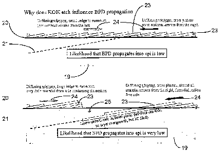
Figure 5 is a schematic diagram of the influence of a KOH etch on the
propagation of basal plane defects.
Figure 6 is a plot of basal plane dislocation density versus surface
preparation
technique.
CA 02539618 2006-03-20
WO 2005/034208 PCT/US2004/030041
Detailed Description
The invention is a method of preparing a substrate for reducing stacking fault
nucleation and reducing forward voltage (Vf) drift in silicon carbide-based
bipolar
devices.
In a first embodiment the method initially comprises conducting a non-
selective etch, preferably a dry etch, most preferably a reactive ion etch
(RIE), on the
surface of a silicon carbide substrate to remove both surface and subsurface
damage
that typically results from the sawing and lapping of the extremely hard SiC
material.
As lmown to those familiar with the manufacture of electronic devices, a
nonselective
etch removes all material at an equal rate. A selective etch removes specific
materials-e.g. damaged, n-type, p-type-more quickly than the other materials.
Exemplary, but not limiting, teclnuques for dry etching of silicon carbide are
set forth
in U.S. Patents No. 4,865,685 and its sibling No. 4,981,551. Other techniques
and
chemistries for carrying out the selective and non-selective etches described
herein
are generally well-recognized in the art and will not be described in detail
herein other
than to illustrate embodiments of the invention.
The term "substrate" is used herein in a sense that is broad enough to include
both a bulls single crystal (usually cut from a boule) as well as a device
precursor
structure that can include one or more epitaxial layers, but which
fundamentally
(although not necessarily exclusively) serves as the physical and electronic
support
for a device formed thereon.
Similarly, the terms "dry etch" and "wet etch" are often used to refer to
reactive ion or plasma etches ("dry") or to etches in molten salts or other
solutions
("wet").
In a preferred embodiment, the initial non-selective etch is carried out to a
depth of approximately five microns. A standard etch, by way of comparison,
only
removes about one micron of material, because a more extensive RIE etch may
tend
to create a laxge number of auto-maslcing defects and pits on the wafer.
Following the nonselective etch, the method comprises conducting a selective
etch on the same surface sufficient to reveal the etch pits of basal plane
dislocations
while avoiding creating beta (i.e., the 3C polytype) inclusions and carrot
defects in
CA 02539618 2006-03-20
WO 2005/034208 PCT/US2004/030041
subsequent epilayer growth. hi preferred embodiments the selective etch is
carned
out with a molten salt, with molten potassium hydroxide (KOH~1~) being one
such
preferred salt. The nature of molten salt etches is generally well understood
by those
of shill in this art and will not otherwise be described in detail. In
somewhat
simplistic terms, the selective etch is the functional opposite of crystal
growth; i.e., in
the same manner that a crystal tends to grow differently at different
structural
features, the etch will tend to remove material differently at different
structural
features, and thus highlight them.
The potassium hydroxide etch is typically carried out for between about 20
and 45 minutes at a temperature of about 450° Centigrade. In
establishing the time
and temperature, an insufficient KOH etch will not sufficiently reveal basal
plane
dislocations. Alternatively, an excessive KOH etching will create 3C (beta)
polytype
inclusions and carrot defects during subsequent epilayer growth on the etched
surface.
In most cases, the temperature of about 450°C beeps the etch
appropriately selective.
A higher temperature etch tends to become non-selective and produce an
undesired
set of resulting broader pits. For example, 600°C appears to be too
high as one
empirical upper limit, while the melting point of the etchant represents the
functional
lower limit.
Performing a mild KOH etch of the substrate after the extended dry etch tends
to further reduce the basal plane dislocation density in epilayers that are
later grown
on the substrate. This improvement is attributed to the different growth
mechanism
over the morphology (etch pit) in the immediate region where the basal plane
dislocation intersects the substrate surface. The KOH etch delineates the
basal plane
immediately down-step from the dislocation. As epilayer growth progresses on
this
surface, there is an enhanced opportunity for the basal plane dislocation to
reorient to
a threading dislocation and thereby reduce the total dislocation length and
also reduce
the free energy of the crystal.
Stated differently, the selective etch helps create a morphology that
encourages dislocations that have originated as basal plane dislocations to
either
terminate or to thereafter propagate (into epilayers) as threading
dislocations. In turn,
the threading dislocations tend to remain unaffected (or at least much less
affected) by
forward voltage during operation of resulting devices.
CA 02539618 2006-03-20
WO 2005/034208 PCT/US2004/030041
9
Following the nonselective and selective etches, the method next comprises
growing a semi-sacrificial epitaxial layer, preferably (but not necessarily)
of n-type
conductivity, on the selectively etched substrate surface to a thickness much
greater
(e.g. at least about 50 percent greater) than that of the typical threadilig
dislocation
etch pit depth (which are generally deeper than basal etch pits) in the
selectively-
etched surface to thereby provide the epitaxial layer with a sufficient
thickness to
support additional polishing and etching steps above the substrate. Once the
semi-
sacrificial layer is sufficient to support the following steps, additional
thickness offers
no extra advantage, and an overly-thick layer adds nothing other than the need
to
remove additional material for its own salve. In preferred embodiments, the
semi-
sacrificial epilayer is about 30-50 microns (~.) thick to provide at least
about 15 ~, for
polishing removal, about 5 ~ for additional RIE removal (these steps are
described
immediately below) and about 10 ~, of improved material remaining as the
desired
epilayer surface.
Generally--but not necessarily--the substrate will be n-type, because n-type
substrates offer a number of advantages in silicon carbide-based devices, and
will
have an activated carrier concentration of about 1E18-1E19 (1 x 101$-1 x 10¹⁹
carriers per cm3). In comparison to the substrate, the carrier concentration
of the
epitaxial layer is selected (or described) in terms of its purpose.
"Conductive" layers
will typically have a Garner concentration of 1E18-19. "Blocking" layers will
typically have carrier concentrations less than lEl6. "Active" layers will
have carrier
concentrations within these parameters, depending on the structure or purpose
of the
end device. Accordingly, although terms such as n, n+ and n- can be used to
describe
both substrates and epilayers, such terminology should be considered in an
illustrative
rather than a limiting sense.
In a next step, the method of the invention comprises polishing away a
sufficient portion of the semi-sacrificial epitaxial layer, typically about 15
~,, to
remove the material containing the etched pits to thereby provide a surface
with fewer
pits than the surface of the original substrate. In preferred embodiments, the
polishing
can be carried out chemically or mechanically or both, with such steps being
generally
well-understood in tlis art.
CA 02539618 2006-03-20
WO 2005/034208 PCT/US2004/030041
In a final preparation step, the method of the invention thereafter comprises
conducting a second non-selective etch (with RIE being typically preferred) of
the
semi-sacrificial epilayer sufficient to remove subsurface damage from the
polishing
step, but without reaclung the underlying substrate, to thereby reduce the
number of
5 subsurface defects that can propagate stacking faults under forward voltage
in a
device formed on the substrate. In a preferred embodiment, the second non-
selective
etch is used to remove about 5 more microns from the semi-sacrificial layer.
Because the method of the invention provides a superior surface for ~epilayer
growth, the method can further comprise forming a bipolar device by forming a
n-
10 type epitaxial layer above the polished and etched surface of the epitaxial
layer, and
forming a p-type epitaxial layer above the polished and etched surface of the
epitaxial
layer, with a p-n junction between the n-type and p-type epitaxial layers. As
used
herein, the phrase "above" a layer can include forming one layer irmnediately
upon
another layer, or on one or more intermediate layers provided that the
intermediate
layers do not otherwise interfere with the layers of interest. Such
intermediate layers
may be included for various structural or functional purposes, including
providing
appropriate buffers and transition layers in a device or device precursor that
do not
otherwise affect the basic design of the desired bipolar device. In this
manner, the
invention can be advantageously incorporated into any semiconductor device
that
experiences Vf drift or performance degradation similar to Vf drift such as
recombination enhanced dislocation glide.
In preferred embodiments, preparing a bipolar device includes the steps of
etching the n-type silicon carbide substrate, growing, polishing and etching
the semi-
sacrificial n+ epitaxial layer on the selectively etched substrate surface,
growing an n-
type epitaxial layer above the polished and etched n+ epitaxial layer, and
growing a p-
type epitaxial layer above the n-type epitaxial layer, with a p-n junction
between the
n-type and p-type epitaxial layers.
The silicon carbide substrate upon which the device is formed can be talcen
from a larger crystal (or "boule"), typically by the steps of sawing a silicon
carbide
substrate wafer from a silicon carbide boule, and thereafter conducting the
nonselective etch on the substrate wafer. In most circumstances, the sawed
substrate
wafer is lapped, polished, etched (typically RIE), and cleaned (with an acid
or
CA 02539618 2006-03-20
WO 2005/034208 PCT/US2004/030041
11
solvent) prior to conducting the first isotropic (nonselective) etch of the
method of the
invention. The term "lapped" is used in its typical sense; i.e., to describe
the steps of
flattening the wafer surfaces using a counter-rotating lapping maclune and an
abrasive
(e.g. diamond) slurry. Lapping helps male the wafer surfaces parallel and
reduces
mechanical defects such as saw marl~ings. Similarly, the polishing etching and
cleaning steps are otherwise carried out conventionally prior to the steps of
the
present invention.
The invention advantageously reduces the density of basal plane dislocations
in the epilayer by a factor of at least two orders of magnitude as compared to
more
conventional techniques. This reduction in basal plane dislocation density
along with
the measures identified to isolate active device regions from the substrate
and surface
defects discussed in previously-referenced publication No. 20030080842
represent a
major step to commercializing SiC bipolar devices.
Additional aspects of the invention can be tulderstood with respect to the
drawings.
Figure 1 is a micrograph of the surface of a silicon carbide epitaxial layer
etched with potassium hydroxide I~OH) and revealing various common types of
dislocation pits. As set forth elsewhere herein, many types of dislocations
can impact
device performance, but the basal plane dislocations are particularly
implicated as
being the prevalent nucleation site of the staclcing faults that cause the
undesired drift
under forward bias. In Figure 1, several (but not necessarily all) of the
basal plane
dislocation etch pits axe designated at 10. A micropipe is designated at 1 l,
a
threading screw dislocation at 12, and threading edge dislocations at 13. The
basal
plane dislocation etch pits are in part identified by having a generally oval
shape with
one frequently faceted edge, with the deepest part of the pit being visible
nearest to
the faceted edge. The micropipe 11 is identified by its generally laxger size
and its
hexagonal geometry characteristic of the crystal pacl~ing structure of silicon
carbide.
The threading screw dislocations are identified with the deepest portion being
at or
near the center of the pit. Because the photographed surface has an 8°
off axis
orientation with respect to the basal plane, the etch pit bottoms in Figure 1
appear
slightly off center.
CA 02539618 2006-03-20
WO 2005/034208 PCT/US2004/030041
12
Figure 2 illustrates a carrot defect 14 (identified by its characteristic
shape,
from which it derives its name) on the surface of the silicon carbide
epitaxial layer.
Figure 3 is a photograph of the surface of Figure 2, following the potassium
hydroxide etch and showing the manner in which the etch delineates the carrot
defect
along with the basal plane dislocations, the threading screws and the
threading edge
dislocations.
Figure 3 illustrates the same surface as Figure 2, but after a KOH etch of the
type used and described herein has developed pits corresponding to the carrot
defect,
as well as to basal plane and threading screw and threading edge dislocations.
Figure 4 illustrates a plurality of etched portions 15 on the surface of a
silicon
carbide epitaxial layer that form when silicon droplets etch the silicon
carbide surface
during epitaxial layer growth.
Figure 5 schematically illustrates the manner in which the selective etch can
favorably influence the propagation of basal plane defects into threading
dislocations.
In Figure 5, the surface of a substrate 19 is designated at 20 and a basal
plane is
designated at 21, and is off axis (8° in preferred embodiments) from
the substrate
surface 20 for other favorable growth purposes. Individual layers of atoms in
the
crystal are designated at 23. During epitaxial growth, "adatoms" (those atoms
from
the source gases that form the growing crystal) represented by the arrows 24
diffuse
across the substrate surface 20 and add to the available sites on the crystal
surface.
Because the crystal is oriented 8 ° off axis, atoms moving from right
to left tend to
add to the crystal more easily and frequently than those moving from left to
right.
When the substrate 19 is etched and an etch pit (designated at 25) develops
from a basal plane dislocation, the resulting morphology creates an even
greater
tendency for diffusing adatoms to add as they move from right to left and an
even
smaller tendency for them to add if moving from left to right. The resulting
growth
tends to favor a threading structure rather than a planar defect and such
threading
structures, as noted previously, appear to have little or no negative effect
when a bias
is applied to a resulting device.
Figure 6 presents some characteristic data from the basal plane dislocation
reduction work, and plots basal plane dislocation density (as described
earlier in pits-
crri 2) on a logarithmic Y-axis against the progressive preparation techniques
for three-
CA 02539618 2006-03-20
WO 2005/034208 PCT/US2004/030041
13
inch wafers along the X-axis. As set forth therein, a typical substrate
includes about
103-105 cm 2 dislocations, following which growing an epitaxial layer reduces
the
density by about an order of magnitude (to about 102-103 cm 2). Using either
RIE or a
molten KOH etch (but not both), the density can be reduced by about another
order of
magnitude (about 40-50 cm 2 in Figure 6), but neither RIE nor KOH shows a
significant improvement over the other. Using the invention, however, the
dislocation
density can be reduced by yet another order of magnitude, i.e., to about 4-5
cm 2 for
the data reported in Figure 6.
In order to take further advantage of the defect reduction in the substrate,
the
growth conditions for later (e.g. device) epilayers can be optimized to
enhance the
likelihood that the basal plane dislocations will become threading
dislocations.
Principally, this involves adjusting pre-etch, starting growth rate, and
stoichiometry to
generate a facile environment for dislocation turning.
Lastly, it is also possible to generate dislocation loops during epilayer
growth.
These loops can contain sections where the dislocation exhibits a basal
character and
these loop segments can decompose into Shockley partials and generate stacking
faults. Epilayer growth conditions must be employed such that the loops do not
form.
In practice this means maintaining adequate surface mobility of adatoms (via
sufficient temperature and stoichiometry) such that there is sufficient time
to
accommodate impinging material properly into the crystal before the additional
depositing layers lock the previously deposited material in place.
The invention focuses on the behavior of a class of dislocations that
historically have not been well addressed in SiC epilayer growth technology.
The
extended etches differ substantially from conventional practice. I~OH etching
or
selectively etching the substrate prior to epilayer growth is very atypical.
Ramping of
growth rate is also unusual especially because doping and crystal quality
control
become problematic during the ramp. However these unusual steps offer the
opportunity to dramatically reduce V f drift as a technology limiting issue.
The impact
of these steps on device properties other than Vf drift remains to be
evaluated.
The removal of damaged material by the extended dry etch can be
accomplished by numerous other approaches. Sputtering, ion-milling, wet
etching
and CMP are some obvious alternatives. Further, refinements in the wafer
shaping
CA 02539618 2006-03-20
WO 2005/034208 PCT/US2004/030041
14
and polishing processes may reduce or eliminate the need for sub-surface
damage
removal.
The selective KOH etch may also be replaced by another etch technique or
may be incorporated into final surface preparation steps or into an in-situ
pre-epilayer
growth treatment.
The approach can be of value for the production of any semiconductor device
which experiences Vf drift or performance degradation similar to Vf drift such
as
recombination enhanced dislocation glide.
The techniques referred to herein are, taken individually, generally well-
recognized and well-understood in the art and can be practiced without undue
experimentation. Single crystal silicon carbide wafers of the type preferably
used as
starting structures herein are commercially available from Cree, Inc. 4600
Silicon
Drive, Durham, North Carolina 27706. The growth of silicon carbide epitaxial
layers
can be carried out using techniques such as those set forth in U.S. Patents
numbers
4,912,063; 4,912,064; 5,679,153; and 6,297,522. Dry and electrolytic etching
of
silicon carbide are described in U.S. Patents numbers 6,034,001; 5,571,374;
5,227,034; 4,981,551; and 4,865,685. The use of molten potassium hydroxide as
an
etchant to identify and characterize a semiconductor surface is well-
understood, and
includes versions expressed as ASTM standards (e.g. ASTM F1404.92). Cutting,
mechanical polishing and lapping of substrate wafers are also entirely
conventional in
this axt.
In the drawings and specification there has been set forth a preferred
embodiment of the invention, and although specific terms have been employed,
they
are used in a generic and descriptive sense only and not for purposes of
limitation, the
scope of the invention being defined in the claims.