Note: Descriptions are shown in the official language in which they were submitted.
CA 02540691 2011-07-26
FLEXURAL PLATE WAVE SENSOR
FIELD OF THE INVENTION
This invention relates generally to flexure plate wave sensors and more
particularly to an improved comb pattern for a flexural plate wave sensor.
BACKGROUND OF THE INVENTION
A flexural plate wave (FPW) sensor includes a diaphragm or plate which is
driven
so it oscillates at frequencies determined by a comb pattern and the flexural
plate
geometry. The comb pattern is disposed over the flexural plate and establishes
electric
fields which interact with the plate's piezoelectric properties to excite
motion. The
eigenmodes describe the diaphragm displacements which exhibit spatially
distributed
peaks. Each eigenmode consists of n half sine periods along the diaphragm's
length. A
typical FPW sensor can be excited to eighty or more eigenmodes. In a typical
FPW
eigenmode, the plate deflection consists of many sinusoidal (or nearly
sinusoidal) peaks.
Prior art flexure plate wave sensors typically include drive combs at one end
of
the plate and sense combs at the other end. The drive combs of these prior art
devices
typically cover only twenty-five to forty percent of the total length of the
plate. When the
CA 02540691 2006-03-29
WO 2005/033660 PCT/US2004/032061
2
number of drive teeth is small compared to the number of eigenmodes peaks, the
small
number of drive teeth can align with several eigenmodes. The result is that
not only are
the eigenmodes perfectly aligned with the comb teeth excited, but other
eigenmodes are
also excited. In signal processing and spectral analysis, this effect is known
as leakage.
A significant drawback of prior designs is that the increased number of
eigenmodes
excited in the FPW sensor produces a series of resonance peaks of similar
amplitude and
irregular phase which increases design complexity and the operation of the
prior art
flexure plate wave sensors.
Moreover, prior art flexural plate wave sensors utilize drive and sense combs
at
opposite ends of the flexural plate and rely on analysis based on an analogy
to surface
acoustic waves (SAW) wherein the waves propagate away from the drive combs and
toward the sense combs and back reflections are regarded as interference. A
distinct
disadvantage of this analysis is that SAW theory does not account for numerous
small
peaks produced by the sensor resulting in calculated gains (e.g., peaks of
similar
magnitude) which are low and do not account for sharp phase drops seen with
the peaks
(e.g., irregular phase).
SUMMARY OF THE INVENTION
It is therefore an object of this invention to provide an improved flexural
plate
wave sensor.
It is a further object of this invention to provide such a sensor which
reduces the
number of eigenmodes excited in the flexural plate.
CA 02540691 2006-03-29
WO 2005/033660 PCT/US2004/032061
3
It is a further object of this invention to provide such a sensor which
outputs a
single pronounced peak, or a peak much larger than any of the other peaks.
- It is a further object of this invention to provide such a sensor which
outputs a
distinct phase.
It is a further object of this invention to provide such a sensor which
simplifies the
operation and design of the sensor.
It is a further object of this invention to provide such a sensor which
improves
stability and performance of the sensor.
It is a further object of this invention to provide such a sensor which
improves
stability by eliminating erroneous readings due to interference created by
mode hopping
from other eigenmodes is eliminated.
This invention results from the realization that a truly effective and robust
flexural
plate wave sensor is achieved by utilizing a unique comb pattern over the
flexural plate
with drive teeth disposed across the entire length of the flexural plate and
which, in one
embodiment, are aligned with all the eigenmodes of the flexural plate
resulting in the
ability to reduce the number of eigenmodes excited in the plate and the output
of a single
pronounced peak with a distinct phase simplifying the operation and design of
the
flexural plate wave sensor.
This invention features a flexural plate wave sensor including a flexural
plate
having a length and a width, and a comb pattern over the flexural plate with
drive teeth
disposed across the entire length of the flexural plate to reduce the number
of eigenmodes
excited in the plate and thereby simplifying the operation and design of the
flexure plate
CA 02540691 2006-03-29
WO 2005/033660 PCT/US2004/032061
4
wave sensor. The sensor may include sense teeth disposed across the entire
length of the
flexure plate interleaved with the drive teeth. In one example, the sense
teeth face in one
direction and the drive teeth face in an opposite direction.
In one embodiment of this invention, the comb pattern is aligned with one
eigenmode of the flexural plate thereby exciting one eigenmode in the plate.
In one
design, the comb pattern allows the sensor to output a single pronounced peak
thereby
improving the performance of the sensor. The comb pattern of this invention
may also
reduce a transfer function of the sensor to a single peak, or a peak much
larger than any
other peak. In one preferred embodiment, the drive teeth are aligned with the
eigenmodes
excited in the flexural plate. The sense teeth may also be aligned with the
eigenmodes
excited in the flexural plate. Typically, the comb pattern provides for
establishing electric
fields which interact with piezoelectric properties of the flexural plate to
excite motion.
The comb pattern may be made of a material chosen from the group consisting of
copper,
titanium-platinum-gold (TiPtAu) metal, titanium-platinum (TiPt), and aluminum.
Typically, the comb pattern is approximately 0.1 gm thick and may include wire
bond pad
areas and ground contacts. In one design, the drive teeth are on the flexural
plate. The
sense teeth may also be on the flexural plate. Ideally, the drive teeth span
across an
entirety of the width of the flexural plate. The sense teeth may also span
across an
entirety of the width of the flexural plate.
The flexure plate wave sensor may include a base substrate, an etch stop layer
disposed over the base substrate, a membrane layer disposed over the etch stop
layer, a
cavity disposed in the base substrate and the etch stop layer, thereby
exposing a portion of
CA 02540691 2006-03-29
WO 2005/033660 PCT/US2004/032061
the membrane layer, the cavity having substantially parallel interior walls, a
piezoelectric
layer disposed over the membrane layer and the comb pattern disposed over the
piezoelectric layer. The piezoelectric layer may be formed from a material
selected from
the group consisting of aluminum nitrite, zinc oxide and lead zirconium
titanate. The
etch stop layer is typically formed from silicon dioxide. Ideally, the
membrane layer is
formed from silicon. In one example, the base substrate is formed from
silicon.
In one design of this invention, the base substrate includes a silicon-on-
insolator
(SOI) wafer, which may include an upper surface of silicon forming the
membrane layer
bonded to an etch stop layer. In other examples, the piezoelectric transducer
may be
deposited over the upper surface of the epitaxial silicon. Ideally, grounding
contacts to
the epitaxial silicon are provided by etching an opening into the
piezoelectric transducer.
In one design, the comb pattern includes titanium-platinum-gold (TiPtAu)
metal. The
comb pattern typically includes interdigital metal electrodes, wire bond pad
areas, and
ground contacts. In an embodiment, the base substrate is approximately 380 gm
thick,
the upper epitaxial surface is approximately 2 gm thick, the layer of Si02 is
approximately 1 gm thick, and the comb pattern is approximately 0.1 gm thick.
The
drive teeth may be approximately 300 to 2000 gm in length and the spacing
between the
drive teeth may be approximately 25 to 50 gm. Typically, the sense teeth are
approximately 300 to 2000 gm in length and the spacing between the sense teeth
is
approximately 25 to 50 gm.
This invention further features a flexural plate wave sensor including a
flexural
plate having a length and a width, and a comb pattern over the flexural plate
with drive
CA 02540691 2006-03-29
WO 2005/033660 PCT/US2004/032061
6
and sense teeth disposed across the entire length of the flexural plate to
reduce the
number of eigenmodes excited in the plate and thereby simplifying the
operation and
design of the flexure plate wave sensor.
This invention also features a flexural plate wave sensor including a flexural
plate
having a length and a width, and a comb pattern over the flexural plate with
first and
second sets of drive teeth disposed across the entire length of the flexural
plate to reduce
the number of eigenmodes excited in the plate and thereby simplify the
operation and
design of the flexural plate wave sensor. In one embodiment the sensor
includes first and
second sets of sense teeth disposed across the entire length of the flexural
plate. The first
and second sets of drive teeth typically face in opposite directions. The
first and second
sets of sense teeth may face in opposite directions. In one design, the first
and second
sets of drive teeth are interleaved. The first and second sets of sense teeth
may also be
interleaved. The first and second sets of interleaved drive teeth may span the
entire
length and approximately fifty percent of the width of the flexural plate. The
first and
second sets of interleaved sense teeth may also span the entire length and
approximately
fifty percent of the width of the flexural plate. Typically, the first and
second sets of drive
teeth face in the same direction, and the first and second sets of sense teeth
face in the
same direction. In one embodiment, the first set of drive teeth is interleaved
with the first
set of sense teeth. The first set of drive teeth interleaved with the second
set of sense
teeth together may span approximately fifty percent of the width of the
flexural plate.
The second set of drive teeth may be interleaved with the second set of sense
teeth. In
other designs, the second set of drive teeth interleaved with the first set of
sense teeth
CA 02540691 2006-03-29
WO 2005/033660 PCT/US2004/032061
7
together may span approximately fifty percent of the width of the flexural
wave plate.
This invention further features a flexural wave plate sensor including a
flexural
plate having a length and a width, and a comb pattern over the flexural plate
with first and
second sets of drive teeth disposed over the flexural plate. Typically, the
first set of drive
teeth span approximately seventy-five percent of the length of the flexural
plate and the
second set of drive teeth span approximately twenty-five percent of the length
of the
flexural plate. The comb pattern reduces the number of eigenmodes excited in
the plate
and thereby simplifying the operation and design of the flexural plate wave
sensor.
In one embodiment, the sensor may include first and second sets of sense teeth
disposed over the flexural plate, the first set of sense teeth spanning
approximately
seventy-five percent of the length of the flexural plate and the second set of
sense teeth
spanning approximately twenty-five percent of the length of the flexural
plate. The first
and second sets of sense teeth may be interleaved with the first and second
sets of drive
teeth. In one example, the first and second sets of drive teeth face one
direction and the
first and second sense teeth face in an opposite direction.
In other designs, the flexural plate wave sensor may include a flexural plate
having a length, width, and a center, and a comb pattern over the flexural
plate with first
and second sets of drive teeth disposed across approximately fifty percent of
the length of
the flexural plate, each set of drive teeth spanning approximately an entirety
of the width
of the flexural plate at one end and curving toward the center of the flexural
plate at
approximately the center of the plate. Ideally, the comb pattern reduces the
number of
eigenmodes excited in the plate and thereby simplifying the operation and
design of the
CA 02540691 2006-03-29
WO 2005/033660 PCT/US2004/032061
8
flexural plate wave sensor. The sensor may also include first and second sets
of sense
teeth disposed across approximately fifty percent of the length of the
flexural plate, each
set of sense teeth spanning approximately an entirety of the width of the
flexural plate and
curving toward the center of the flexural plate at approximately a middle of
the plate.
This invention also features a flexural wave plate sensor including a flexural
plate
having a length and a width, and a comb pattern over the flexural plate. The
comb pattern
may include drive teeth and sense teeth disposed over the flexural plate. The
drive teeth
may span approximately fifty percent of the length of the flexural plate. The
sense teeth
may span approximately the fifty percent of the length of the flexural plate.
Ideally, the
comb pattern reduces the number of eigenmodes excited in the plate and thereby
simplifying the operation and design of the flexural plate wave sensor.
This invention further features a flexural wave plate sensor with a flexural
plate
having a length and a width, and a comb pattern over the flexural plate. The
comb pattern
may include a set of drive teeth and a set of sense teeth. The set of drive
teeth and the set
of sense teeth may be disposed over the flexural plate. The drive teeth may
span
approximately fifty percent of the length of the flexural plate, and the sense
teeth may
span approximately fifty percent of the length of the flexural plate. Ideally,
the comb
pattern reduces the number of eigenmodes excited in the plate and thereby
simplifying the
operation and design of the flexural plate wave sensor.
This invention also features a method for manufacturing a flexural plate wave
sensor, the method including the steps of depositing an etch-stop layer over a
substrate,
depositing a membrane layer over the etch stop layer, depositing a
piezoelectric layer over
CA 02540691 2006-03-29
WO 2005/033660 PCT/US2004/032061
9
the membrane layer, forming a comb pattern with drive teeth which span across
an entire
length of the piezoelectric layer on the piezoelectric layer, etching a cavity
through the
substrate, the cavity having substantially parallel interior walls, and
removing a portion of
the etch stop layer between the cavity and the membrane layer to expose a
portion of the
membrane layer. The method of the manufacturing of a flexural plate wave
sensor of this
invention may further include the steps of etching a hole in the piezoelectric
and forming
a ground contact on the silicon membrane layer.
This invention further features a method for manufacturing a flexural plate
wave
sensor, the method including the steps of depositing an etch-stop layer over a
substrate,
depositing a membrane layer over the etch stop layer, depositing a
piezoelectric layer over
the membrane layer, forming a comb pattern on the piezoelectric layer, the
comb pattern
including drive and sense teeth which span an entire length of the membrane
layer,
forming a second transducer on the piezoelectric layer, spaced from the first
transducer,
etching a cavity through the substrate, the cavity having substantially
parallel interior
walls, removing the portion of the etch stop layer between the cavity and the
membrane
layer to expose a portion of the membrane layer, and depositing an absorptive
coating on
the exposed portion of the membrane layer.
The method of manufacturing a flexural plate of this invention may further
include the steps of etching a hole in the piezoelectric and forming a ground
contact on
the silicon membrane layer.
CA 02540691 2006-03-29
WO 2005/033660 PCT/US2004/032061
BRIEF DESCRIPTION OF THE DRAWINGS
Other objects, features and advantages will occur to those skilled in the art
from
the following description of a preferred embodiment and the accompanying
drawings, in
which:
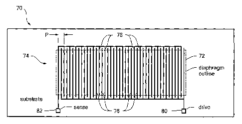
Fig. 1 is a schematic top view of a prior art flexural plate wave sensor
showing
drive and sense combs extending over approximately twenty-five to forty
percent of the
flexural wave plate;
Fig. 2 is a graph showing the relationship of eigenmodes displacements to
drive
teeth for the sensor shown in Fig. 1;
Fig. 3A is a graph showing the typical output for the wave sensor shown in
Fig. 1;
Fig. 3B is a graph showing the irregular phase response for the peaks shown in
Fig. 3A;
Fig. 4 is a schematic side view showing the direction of wave propagation of
the
sensor shown in Fig. 1;
Fig. 5 is a schematic top view of one embodiment of the flexural plate wave
sensor in accordance with the subject invention;
Fig. 6A is a graph showing a single pronounced peak output by the flexural
plate
wave sensor shown in Fig. 5;
Fig. 6B is a graph showing a distinct phase response for the peak shown in
Fig. 6A;
Fig. 7A is another graph showing several pronounced peaks of various magnitude
output by the flexural plate wave sensor shown in Fig. 5;
CA 02540691 2006-03-29
WO 2005/033660 PCT/US2004/032061
11
Fig. 7B is a graph showing a distinct phase response for the peaks shown in
Fig. 7A;
Fig. 8 is a schematic side view showing the various layers of the flexural
plate
wave sensor of this invention;
Fig. 9 is a schematic top view of another embodiment of the comb pattern of
the
flexural plate wave sensor of this invention;
Fig. 10 is a schematic top view of another example of a comb pattern for the
flexural plate wave sensor of this invention;
Fig. 11A is a schematic top view of another design of the comb pattern of the
flexural plate wave sensor of this invention;
Fig. 11B is a schematic top view of another design of the comb pattern of the
flexural plate wave sensor of this invention;
Fig. 12 is a schematic top view of yet another design of the comb pattern of
the
flexural plate wave sensor of this invention;
Fig. 13 is a flowchart showing the primary steps associated with one method of
manufacturing a flexural plate wave sensor in accordance with this invention;
Fig. 14 is a schematic diagram of the circuitry associated with one embodiment
of
the flexural plate wave sensor in accordance with the subject invention;
Figs. 15A-15C are graphs showing several examples of the output of the
flexural
plate wave sensor of the subject invention;
Figs. 16A-16F are a listing of the MATLAB code for a three-mode frequency
response of one embodiment of the flexural plate wave sensor of this
invention;
CA 02540691 2006-03-29
WO 2005/033660 PCT/US2004/032061
12
Fig. 17 is a graph showing the relative eigenfrequencies of one embodiment of
the
flexural plate wave sensor of this invention; and
Fig. 18 is a graph showing the static plate deflections for a sinusoidal load
on the
flexural plate wave sensor of this invention.
DISCLOSURE OF THE PREFERRED EMBODIMENT
Aside from the preferred embodiment or embodiments disclosed below, this
invention is capable of other embodiments and of being practiced or being
carried out in
various ways. Thus, it is to be understood that the invention is not limited
in its
application to the details of construction and the arrangements of components
set forth in
the following description or illustrated in the drawings.
As discussed in the Background section above, prior art flexure plate wave
sensor
10, Fig. 1 includes drive comb 14 with drive teeth 16 and 18 and drive comb 20
with
drive teeth 22 and 24. Typically, drive combs 14 and 20 are driven at opposite
polarity,
e.g., drive comb 14 is driven at a positive polarity and drive comb 20 is
driven at a
negative polarity, to align with the positive and negative peaks of the
eigenmodes.
As shown in Fig. 1, drive combs 14 and 20 are disposed over only approximately
twenty-five to forty percent of the entire length of flexural plate 38.
Because of the
limited length extent of drive combs 14 and 20, there is a limited number of
drive teeth,
e.g., drive teeth 16, 18, 22, and 24. As discussed in the Background section
above, when
the number of drive teeth is small compared to the number of eigenmode peaks
of the
flexural plate 38, several eigenmodes will be excited.
CA 02540691 2006-03-29
WO 2005/033660 PCT/US2004/032061
13
For example, Fig. 2 shows the modal displacement for longitudinal eigenmodes,
with n = 20 and n = 21, (where n = mode number = 1/2 sine'periods) of flexural
plate 38
shown in Fig. 1. As shown in Fig. 2, there is limited number of drive teeth
16, 18, 22,
and 24 relative to the number of eigenmodes peaks 39 and 41. The result is
that not only
are the n = 20 eigenmodes perfectly aligned with the drive teeth 16, 18, 22,
and 24
excited, but other eigenmodes are also excited, as shown by arrows 43, 45, 49,
and 51.
The increased number of eigenmodes excited produces a series of resonance
peaks of
similar amplitude as shown by peaks 60, 62, 64 and 66, Fig. 3A, and irregular
phase, as
shown in Fig. 3B. The result is increased complexity in the electronic design
and
operation of prior art flexural plate wave sensor 10.
Prior art sensor 10, Fig. 1 also includes sense comb 26 and 32, typically at
the
opposite end of flexural plate 38 from drive combs 14 and 26, with sense teeth
28, 30,
and 34, 36, respectively. As discussed above in the Background section, prior
art sensor
relies on a theory based on surface acoustic waves (SAW) wherein waves
propagate
away from drive combs 14 and 20 toward sense combs 26 and 32, as indicated by
arrow
50, Fig. 4, and back reflections are regarded as interference. Reliance on SAW
theory,
however, does not account for numerous small peaks produced by sensor 10,
results in
calculated gains which are low, and cannot account for sharp phase drops.
In contrast, flexural plate wave sensor 70, Fig. 5 of the subject invention
includes
flexural plate 72 having a length and a width, and comb pattern 74 over
flexural plate 72
with drive teeth 76 disposed across the entire length of flexural plate 72 to
reduce the
number of eigenmodes excited in plate 72. In one design, comb pattern 74 is
aligned with
CA 02540691 2006-03-29
WO 2005/033660 PCT/US2004/032061
14
all the eigenmodes of flexural plate 72. In a preferred embodiment, only one
eigenmode
is excited. The result is that flexural plate wave sensor 70 outputs a single
pronounced
peak, e.g., peak 80, Fig. 6A, with a distinct phase, as shown in Fig. 6B, or a
pronounced
peak much larger than any of the other peaks, e.g., peak 82, Fig. 7A, compared
to peaks
84, and 86, with a distinct phase, as indicated by arrow 89, Fig 7B. This is
in stark
contrast to the peaks of similar amplitude and irregular phase produced by
prior art
sensors, as shown in Figs. 3A and 3B. The result is a significant
simplification in the
operation and design of flexural plate wave sensor 70, Fig. 5. With only a
single mode
capable of being excited, the design of closed loop electronics of this
invention, discussed
below, improves stability of the system because erroneous readings do to
interference
created by mode hopping from other eigenmodes (as shown in Figs. 3A and 3B) is
not
possible.
In one design in accordance with this invention, sensor 70 further includes
sense
teeth 78 disposed across the entire length of flexural plate 72. In one
embodiment, sense
teeth 78 and drive teeth 76 face in opposite directions. In this design, sense
teeth 78 are
interleaved with drive teeth 76. Sense teeth 78 are typically aligned with the
eigenmodes
excited in flexural plate 72 to detect the output produced by drive teeth 76.
In one example of this invention, comb pattern 74 is made of copper. In other
examples, comb pattern 74 is made of titanium-platinum-gold (TiPtAu), titanium-
platinum (TiPt), aluminum, or any known materials or combination of materials
known to
those skilled in the art. Typically, comb pattern 74 is approximately 0.1 m
thick and
includes wire bond pad areas 80, and 82, Fig. 5.
CA 02540691 2006-03-29
WO 2005/033660 PCT/US2004/032061
Flexural plate wave sensor 70 is typically comprised of several layers as
shown in
Fig. 8. Sensor 70 may include base substrate 100, typically a silicon
substrate 380 m
thick and etch stop layer 102, ideally 1 gm thick and made of silicon-oxide
(Si02)
disposed over base substrate 100. Ideally, sensor 70 also includes membrane
layer 104,
typically made of silicon or similar material and is disposed over etch stop
layer 102 and
cavity 106. Additional silicon is typically grown to form membrane layer 104
(e.g.,
diaphragm layer). Cavity 106 has substantially parallel interior walls and is
disposed
within base substrate 100 and etch stop layer 102 thereby exposing a portion
of
membrane layer 104. In one example, piezoelectric layer 108 with a thickness
of 0.5 gm
is disposed on membrane layer 104. Comb pattern 74 with drive teeth 76 and
sense teeth
78 (as also shown in Fig. 5) is disposed over piezoelectric layer 108.
Typically, layer 104
is connected to ground (not shown). Piezoelectric layer 108 is ideally formed
from a
material such as aluminum nitride, zinc oxide, and lead zirconium titanate.
In other designs, base substrate 100 is a silicon-on-insulator (SOI wafer) and
includes upper surface of silicon (e.g., membrane 104) bonded to etch stop
layer 102.
Ideally, grounding contacts to silicon layer (e.g., membrane 104) are provided
by etching
an opening into piezoelectric layer 108. In one preferred example, titanium-
platinum-
gold metal or titanium-platinum is patterned to define comb pattern 74, Fig. 5
with drive
teeth 76 and sense teeth 78 disposed across the entire length of piezoelectric
layer 108,
Fig. 8. Ideally, comb pattern 74 further defines wire bond pad areas 80 and
82, Fig. 5 and
grounding contacts (not shown). Typically, drive teeth 76 and sense teeth 78
are 300 gm
to 2000 m in length and the spacing between the drive and sense teeth is
approximately
CA 02540691 2006-03-29
WO 2005/033660 PCT/US2004/032061
16
25 to 50 m.
As shown above, the unique design of comb pattern 74 of flexural plate wave
sensor 70 with drive teeth 76 disposed across the entire length of flexural
plate 72
effectively reduces the number of eigenmodes excited in the flexural plate and
outputs a
single pronounced peak, or a peak much larger than any of the other peaks
output by
sensor 70. The result is a simplification in the operation and design of
flexural wave
plate sensor 70.
Unique comb pattern 74 may take several forms including sets of interleaved
drive teeth and interleaved sense teeth which each span the entire length and
approximately fifty percent of the width of the flexural plate (Fig. 9), two
sets of
interleaved drive and sense teeth wherein each set of interleaved drive and
sense teeth
spans the entire length and approximately fifty percent of the width of the
flexural plate
(Fig. 10), two sets of interleaved drive and sense teeth wherein one set of
interleaved
drive and sense teeth spans approximately seventy-five percent of the length
of the
flexural plate and the other set spans approximately twenty-five percent of
the flexural
plate (Fig. 11), and unique curved sets of drive and sense teeth (Fig. 12).
Other
equivalent embodiments may occur to those skilled in the art.
Comb pattern 74', Fig. 9 includes first set 120 of drive teeth and second set
124 of
drive teeth disposed across the entire length of flexural plate 72. Comb
pattern 74' may
also include first set 128 of sense teeth and second set 130 of sense teeth
also disposed
across the entire length of flexural plate 72 and are used to sense the output
provided by
first set 120 and second set 124 of drive teeth. In one example, first set 120
of drive teeth
CA 02540691 2006-03-29
WO 2005/033660 PCT/US2004/032061
17
is driven at a negative polarity and second set 124 of drive teeth is driven
at a positive
polarity to align with the negative and positive peaks of the eigenmodes of
flexural plate
72 and aid in the reduction of eigenmodes excited. Similarly, first set 128 of
sense teeth
is driven at a positive polarity and second set 130 of sense teeth is driven
at a negative
polarity. First set 120 and second set 124 of drive teeth may face in opposite
directions
and are interleaved with each other. Similarly, first set 128 and second set
130 of sense
teeth face in opposite directions and are interleaved with each other. In this
design, first
set 120 of drive teeth is interleaved with second set 124 drive teeth which
together are
disposed across the entire length of flexural plate 72 and span approximately
50 percent
of the width of flexural plate 72. Similarly, first set 128 of sense teeth is
interleaved with
second set 130 of sense teeth which together are disposed across the entire
length of
flexural plate 72 and span the remaining 50 percent of the width of flexural
plate 72. The
design of comb pattern 74' not only reduces the number of eigenmodes excited
but also
helps reduce the number of peaks output by sensor 70'.
In another example of this invention, the design of comb pattern 74' described
above is modified to interleave the first set of drive teeth with the first
set of sense teeth
as shown in Fig. 10. Comb pattern 74" includes first set of drive teeth 131
interleaved
with first set of sense teeth 132. Interleaved sets 131 and 132 are disposed
across the
entire length of flexural plate 72 and fifty percent of the width of flexural
plate 72. Comb
pattern 74" also includes second set of drive teeth 134 interleaved with
second set of
sense teeth 136, which similarly span the entire length of flexural plate 72
and fifty
percent of the width of flexural plate 72. Typically the sets of drive teeth
(e.g., sets 131
CA 02540691 2006-03-29
WO 2005/033660 PCT/US2004/032061
18
and 134) and the sets of sense teeth (e.g., sets 132 and 136) are driven at
opposite
polarities. Similar to the above design in Fig. 9, this design not only
reduces the number
of eigenmodes excited but also reduces the number of peaks produced by sensor
70.
In yet another design, comb pattern 74"', Fig. 11A includes first set 150 of
drive
teeth and second set 152 of drive teeth. First set 150 spans approximately 75
percent of
flexural plate 72 and second set 152 spans approximately 25 percent the length
of flexural
plate 72. Comb pattern 74"' may further include first set 154 of sense teeth
which spans
approximately 75 percent of the length of flexural plate 72 and is interleaved
with first set
150 of drive teeth. Comb pattern 74"' may also include second set 154 of sense
teeth
which span approximately 25 percent of the length of flexural plate 72 and is
interleaved
with second set 152 of drive teeth. This design also reduces the number of
eigenmodes
excited in flexural plate 72.
In one embodiment, comb pattern 74'v, Fig. 11B may include drive teeth 170 and
sense teeth 172 disposed over flexural plate 72. Drive teeth 170 span
approximately fifty
percent of length of the flexural plate 72, as indicated by arrow 174, and
sense teeth 172
span approximately fifty percent of the length of flexural plate 72, as
indicated by arrow
176. Comb pattern 74'" similarly reduces the number of eigenmodes excited in
flexure
plate 72.
In another design, comb pattern 74'" may include set of drive teeth 173 which
includes drive teeth 170 and drive teeth 171. Set of drive teeth set 173 spans
approximately fifty percent of the length of flexural plate 72, similarly
indicated by arrow
174. Comb pattern 74"' also includes set of sense teeth 175 which includes
sense teeth
CA 02540691 2006-03-29
WO 2005/033660 PCT/US2004/032061
19
172 and sense teeth 177. Set of sense teeth set 175 spans approximately fifty
percent of
the length of flexural plate 72, as indicated by arrow 176. This design also
reduces the
number of eigenmodes excited in flexural plate 72. Although as shown in Fig.
11B, set
of drive teeth 173 includes drive teeth 170 interleaved with drive teeth 171
and set of
sense teeth 175 includes sense teeth 172 interleaved with sense teeth 177,
this is not a
necessary limitation of this invention, as drive teeth (e.g., drive teeth 170
or drive teeth
171) may also be interleaved with the sense teeth (e.g., sense teeth 172 or
177).
In another design in accordance with this invention, comb pattern 74`', Fig.
12
includes first set 160 of drive teeth and second set 162 of drive teeth
disposed across
approximately 50 percent of the length of flexural plate 74. First set 160 and
second set
162 of drive teeth span approximately the entire width of flexural plate 74 at
one end and
curve downward towards center 164 of flexural plate 74. The unique design of
comb
pattern 74" helps reduce the number of eigenmodes excited in the plate and
also aids in
reducing the number of peaks output by sensor 70. Comb pattern 74" may also
include
first set 166 of sense teeth interleaved with second set 168 of sense teeth of
similar
configuration to first and second sets 160, and 162 of drive teeth as
described above.
The method for manufacturing the flexural plate wave sensor 70 of this
invention
includes the steps of. depositing an etch top layer 102, Fig. 8 over substrate
100, step 200,
Fig. 13; depositing (e.g., growing additional silicon) membrane layer 104,
Fig. 8 over etch
top layer 102, step 202, Fig. 13; depositing piezoelectric layer 108, Fig. 8
over membrane
layer 104, step 204, Fig. 13; forming comb pattern 74, Fig. 8 (and Figs. 5,
and 9-11) on
piezoelectric layer 108 with drive teeth 76 which span across the entire
length, or portion
CA 02540691 2006-03-29
WO 2005/033660 PCT/US2004/032061
thereof, of piezoelectric layer 108, step 206, Fig. 13; and etching cavity
106, Fig. 8
through substrate 100 between cavity 106 and membrane layer 104 to expose a
portion of
membrane layer 104, step 208, Fig. 13. In other examples, a silicon-on-
insulator wafer
(SOI) is employed which includes the oxide layer (e.g., etch stop layer 102)
and the
silicon diaphragm layer (e.g., membrane layer 104) already bonded together.
As shown above, the robust flexural plate wave sensor of the subject invention
includes a comb pattern of several unique configurations which is disposed
across the
entire length of the flexural wave plate and reduces the number of eigenmodes
excited in
the plate thereby providing for a simple operation and design of the flexural
wave plate.
The unique comb pattern with drive teeth that span the entire length of the
flexural wave
plate provides the ability for the comb pattern to be aligned with the
eigenmodes of the
flexural wave plate. The result is the ability for flexural plate wave sensor
70 to produce
a single pronounced peak, or a peak much larger than any of the other peaks,
and provide
greater stability, improved performance, and simplification of the design of
the flexural
plate wave sensor.
As stated in the Background section above, prior art sensor 10, Fig. 1
utilizes
drive combs 14 and 20 and sense combs 26 and 32 at opposite ends of the
flexural plate.
Prior art sensor 10 relies on theory based on an analogy to surface acoustic
waves (SAW)
wherein the waves propagate away from the drive combs 14 and 20 toward the
sense
combs 26 and 32, as shown in Fig. 4, and back reflections are regarded as
interference.
The inventors hereof realized that such an analogy to SAW was incorrect for
most
flexural plate wave devices. In particular, design with simple edge
conditions, such as the
CA 02540691 2006-03-29
WO 2005/033660 PCT/US2004/032061
21
flexural plate shown in Fig. 14 and Figs. 9-11, actually behaves as a
resonating plate. The
analysis below, equations (1) through (14), is based on modeling flexural
plate 302,
Fig. 14 as a thin beam. Comparisons to product performance and calculations of
flexural
plate 302 eigenfrequencies indicate that the beam model is valid for
resonating plate 302
and sensor 300, as well as sensor 70 as shown in Figs. 5 and 9-11. Equations
(16) and
(17) below augment the simple beam model to consider additional modes across
the
flexured plate 302 thickness.
As shown in Fig. 14, the drive voltage of flexural wave plate sensor 300,
which
includes flexural plate 302, is referenced to zero and applied to center
grounded
transformer 304 which applies +VD to one electrode and -VD to the other. The
input side
of the transformer 304 is connected to ground 306 and VD. The output side is
center
tapped so that the ends are +VD and -VD. In another example of this invention,
one port
operation may be employed using the drive circuit as an output, such as with a
Pierce or
series oscillator as known to those skilled in the art. A drive pair consists
of two
electrodes, e.g., electrodes or drive combs 350 and 352 at +VD and -VD. A
sense pair
may consist of two electrodes or sense combs, e.g., electrodes or sense combs
354 and
356, which are typically connected to the inputs of differential amplifiers,
such as
differential amplifiers 355 and 357, respectively. In one design, all the
electrodes, e.g.,
electrodes or combs 350, 352, 354 and 356 are deposited on top of the
piezoelectric layer
(not shown) of flexural plate 302. (Similar to the design of flexural plate
70, Fig. 8
discussed above.) Silicone layer 309, Fig. 14 is typically connected to ground
306.
The relationship between the eigenmodes and flexural plate voltage is shown
CA 02540691 2011-07-26
22
below. The derivation of equation (1) below is disclosed in "Modeling Flexural
Plate
Wave Devices", Weinberg et al., Journal of Microelectro Mechanical Systems,
Vol. 9,
(September 2000). The following equations are based on a thin beam vibrating
in the z
direction as shown in Fig. 14. The displacement at any position is given by:
z(t) = A. (t)cn (x) (1)
n=1
The equation of motion for each mechanical mode is:
X
I p. (x)f(x,t)dx
in, Ak. +bl +mm2Aõ = f, (t) (2)
2(x)dx
where 4(x) szs sin(2nx- 4) = eigenmode shape for built-in diaphragm edges,
which
equals sin(. x) for simple supports, A. = 2nL 1 it equals eigenvalue for built-
in edges,
and An = n7r is the eigenvalue for simply supported edges. Further, where n is
a positive
integer equal to the number of half wavelengths in length L, mp is the mass
per unit
length, b is the damping per unit length, A. is the amplitude of motion of the
excited n'th
mode, L is flexural plate length, and (t) is the forcing function for mode n.
For simple and built-in supports, the angular resonant frequency is related to
the
wave number A, by.
(3)
O)n = rnm~
CA 02540691 2006-03-29
WO 2005/033660 PCT/US2004/032061
23
where D is the rigidity.
Assuming the mode shape is given by:
cPõ (x) = sing n - co) (4)
Also assume pinned beams for which cp = 0. Because of the large number of
modes,
pinned and built-in beams differ little. Assume also that the beam is driven
by a force
density whose first harmonic is:
w(x, t) = w Q sin( P - J sin(cot) (5)
where w0 _ - 2r2 m ~ t 2 MpY D, MP is the magnitude of piezoelectric torque
per volt
7r ( applied to electrodes, VD is the voltage applied to drive teeth 352, 0 is
the alignment
between comb fingers and reference, 2t is length of transducer which equals
mP/2, P is
the comb pitch, and in is number of combs in transducer or the number of half
sines in Lt.
With equations (2), (4) and (5), the modal forcing function is determined
from:
fn (t) = wõ sin(cot) 2 x, J sing fl - rp I sin j - - 0 dx (6)
xo o
where the comb starts at x, and ends at xo + at . From equation (6) yn is
defined and
relates the modal force to the input voltage:
2 xa+X
2, mac 2 IM mzzx
sin - dx (7)
kõ yn = - Mn sin(c)t) sin - (P
D t xo t
Equation (7) applies to both the comb and sense electrodes, e.g., comb pattern
350 with
CA 02540691 2006-03-29
WO 2005/033660 PCT/US2004/032061
24
drive teeth 350 and 352, and sense teeth 354 and 356 (or any of the designs
shown in
Figs. 5 and 9-12). The integral is taken over the transducer length Xt as
shown in Fig. 11,
since the combs exert the force. With simple support, cp is equal to 0. The
units of y are
m/V and y is proportional to 1/x,,,4. When the combs and modes are aligned, 0
is equal to
0 and the forcing function is:
sin C -mmg sin[( +m~'z
fõ (t) = w,, sin(wt) ?~ n 1 (8)
n
-m)7 C +ml/z
The model amplitudes responses fõ (t)/[Wa sin(cot)] for phase 0 of zero, n/4,
and 7C/2
are shown in Figs. 15A-I5C with a transducer length of 0.00125 meters,
flexural plate
302, Fig. 14 a length of 0.005 meters, and in equals 50, yielding a 50 pm
pitch. When the
wavelength of the eigenmode matches the comb pitch, the maximum forcing of
flexural
plate wave sensor 300 is achieved.
In accordance with this invention, when the drive length, e.g., the length of
comb
pattern 300 with drive teeth 352 (or the designs shown in Figs. 5 and 9-11)
disposed
across the entire length of flexural plate 302, only one mode in the x
direction is excited
and the response becomes a simple second order system, producing a single
pronounced
peak, as shown in Fig. 6A. Moreover, by varying the comb length and tooth
width it is
possible to trim the piezoelectric bending as a function of y which can force
harmonics so
that the y direction sinusoid harmonics are not excited.
In equation (8), the force per length w(x,t) was represented by its first
harmonic.
The modal forcing function fõ (t) in equation (6) is dominated by terms with
denominators
CA 02540691 2006-03-29
WO 2005/033660 PCT/US2004/032061
which include thus, higher harmonics of w(x,t) have larger values of in and
contribute little to equation (8).
Coupling of beam modes into output utilizes the conversion of strain into
charge
on the flexural plate 302, Fig. 14. Assuming flexural plate 302 is grounded,
the surface
charge per unit length is described by:
Q, =d31Ybep(l+Vp) (9)
where d3i is the piezoelectric constant relating z electric field to x strain,
Y is Young's
modulus of the piezoelectric material, vP is Poisson's ratio and b is the
width of
diaphragm.
Using equations (1) and (4), the peak x strain at area center for
piezoelectric
material, Ep, is related to the modal amplitudes by:
_ P) (10)
sp = Az. = 9'z tam = -~(nc~2 Ay,,, A,, ( t ) mix
R &2 where hzm is the distance between the piezoelectric material's center of
area and the
flexural plate's neutral axis for torque inputs, and R = radius of curvature
at position.
The total charge is calculated by integrating equation (9) over the electrodes
(e.g.,
comb patterns 350 and 352, Fig. 14). Because of the sine function in equation
(10), this
integration is similar to a Fourier transform so that is easier to consider
the first
harmonics of the plate distribution:
Q = SQ.dx -- - SQ sin M=
- 8 &C (11)
electrodes x x X t
CA 02540691 2006-03-29
WO 2005/033660 PCT/US2004/032061
26
With equations (9) and (10) inserted into equation (11), the total charge on
the
sense or drive electrodes (e.g., drive teeth 350 and 352 or sense teeth 354
and 356) is:
Q(12)
n
where the coupling between modal amplitude and charge is given by:
r ra 9 Z X, 2 x +'" r n ~zx 1 In 71X an = -I I d31Yb~zf sin( - rpJ sin - 8 dx
(13)
The integral in brackets is identical to that used to calculate the modal
force of
equation (7). The units of an are Coul/m and an is proportional to ~'n2
Insert the piezoelectric diaphragm model into a lumped parameter model with
other electrical circuit elements as follows. The piezoelectric comb pair, for
example
349, typically includes two electrodes, e.g., 350 and 352, and ground plane
306. For a
single mode, the static equation relating modal displacement and charge to
electrode
voltage and modal force is:
1 0 -an
2 QD1 C+ C12 - C12 0 VD1
0 1 2 QDZ = - C12 C + C12 0 VD2 (14)
0 0 1 An 7n Yn 1 /n
2 2 kõ
where C is capacitance from one plate to ground, Cu is capacitance between
positive and
negative electrodes, a,,, yõ are piezoelectric coupling coefficients defined
in equations (7)
and (13), kõ = modal stiffness, Di refers to a positive drive electrode, e.g.,
drive teeth 350,
and D2 refers to a negative drive electrode 352. The negative signs on aõ and
yõ indicate
CA 02540691 2006-03-29
WO 2005/033660 PCT/US2004/032061
27
that the negative electrodes are displaced 180 degrees from the positive
electrodes. The
voltage applied to the negative comb is minus that applied to the plus
electrodes:
VD = VD1 = -VD2 (15)
With small coupling assumption implicit in equation (14), the voltages and
currents applied to flexural plate plates are still described by equations (9)
through (13).
Equation (14) formulation results in QD2 = -QDI which is consistent with the
circuit
diagram of Fig. 14. QDl is the integral of the current 12 defined above.
Symmetry and
differential read out define:
Q=QD1-QD2 (16)
Equation (16) is simplified to:
1 - aõ Q 2(C + 2C12) 0 1 [VD]
(17)
0 1 An yn Jn
k,, When adding the circuit resistors, the Q consists of two currents as
outlined in
equation (16). Equations (16) and (17) describe both the drive and sense
electrode pairs.
The charge is the total charge summed over the electrode while the force is
the
modal force which is a force per unit length along the beam. When the mode
period
matches the combs' period:
n 1,r m;r
and the combs are aligned with the eigenmode [0 equals 4 in equation 7], the
piezoelectric equation (17) obeys a form of reciprocity as shown by:
CA 02540691 2006-03-29
WO 2005/033660 PCT/US2004/032061
28
2aõ
Yõk (19)
The reciprocity demonstrates a symmetry between voltage, modal force, charge
per
length, and modal amplitude. When the eigenmodes are not aligned with the
combs,
equation (19) does not govern.
The results of the above are combined into a comprehensive dynamic flexural
plate wave sensor of this invention which relates excitation voltage to the
preamplifier
output. For clarity, only 3 modes are included in this example. However, this
is not a
necessary limitation of this invention, as any number of modes maybe included
by those
skilled in the art and shown in Figs. 3A, 3B, 6A, 6B, 7A and 7B. As stated
above, the
charge includes both the plus and minus plates. The voltage and force applied
directly to
the piezoelectric material are shown as:
1 0 ; - aD1 - aD2 ' - aD3 QD CD 0 0 0 0 VD
0 1 - as1 as2 as3 Qs 0 Cs 0 0 0 Vs
0 0 k1 0 0 Al = k17D1 k1751 1 0 0 f1 (20)
2
J[ j
0 0 r 0 t k2 0 A2 k27D2 k2752 0 1 0 f2
A
00- 0 1 0 - k3
3 7D3 k37S3 0 0 1 {'
3 k
3
The force applied to the piezoelectric material is described by.
=-bõA-nzpAk (21)
The voltage applied to the drive comb 350, Fig. 14 is:
VD = V - sQDRD (22)
where V= voltage applied by the source and RD is the input resistor.
CA 02540691 2006-03-29
WO 2005/033660 PCT/US2004/032061
29
Assuming that the output preamplifier is at virtual ground, the sense voltage
is
given by:
VS = -sQs 2 (23)
where R5 is the sense resistor. The factor of two accounts for the definition
of Q of
equation (15) which includes both the positive and negative electrodes. The
MATLAB
code for equations (20) through (23) to obtain frequency responses is shown in
Figs.
16A-16C.
As a first approximation for a rectangular plate, e.g., flexural plate 302,
Fig. 14
the eigenmodes in the x and y directions are close to those derived from beam
theory as
shown by J. Blevins, Formulas for Natural Frequency and Mode Shape, Robert E.
Krieger Publishing Co., Malabar, FL (1979). The displacement is a sinusoid in
x
multiplied by a sinusoid in y. For an isotropic or orthotropic rectangular
plate built-in or
simply supported on four edges, the eigenfrequencies (in Hz) are given
approximately by:
G(n)4 G(m)4 2J(n)J(m) Yh3 (24)
,tm = 2 ~4 b4 ~,zbz 12ma (1- vz )
where n is the mode number along length, in is the mode number across width, X
= length
of plate, in one example 0.005 in, b is the width of plate, such as 0.001 in,
G(n) equals n
for simple supports and n+1/2 for all edges built-in, J(n) = n2 for simple
support and is
z
equal to Cn + I J 1- 2 with all edges built-in, Y is Young's modulus, h is the
9(n + 12J
CA 02540691 2006-03-29
WO 2005/033660 PCT/US2004/032061
plate thickness and ma = mass per unit area.
For a simply supported plate, equation (24) becomes:
Yh3 n2 +m2 (25)
/ ,zm 2 12m. 1- V Z x2 b z
For the nominal case, the eigenfrequencies relative to in = 0 and simple
support
are plotted versus in in Fig. 17. For 2,, / b = 5. Equations (24) and (25)
duplicates beam
theory when in = 0. The built-in eigenfrequency is 0.50 % higher than the
simple
support. With in = 1 and n = 200, the built-in's resonant frequency is 0.085 %
larger than
the in = 0 simple beam case. This in =1 frequency is near the beam theory
value and is
the basic operating frequency. As shown in Fig. 18, displacements are close to
the m = 1
mode shape. Higher in modes are more half sines in the y (short) direction.
With in = 2,
the next resonance is 0.21% above the basic operating frequency (m = 1). With
straight
teeth, the excitation is an odd harmonic and should not be excited (except for
fabrication
deviations). For built-ins, the in = 3 resonance is 0.6 % higher than the
fundamental.
Although the excitation is square in the y direction, the response along a
fixed x is largely
sinusoidal as shown in Fig. 18. With square drive the third harmonic of the
drive is 1/3
the fundamental. Fig. 3A shows a raggedness associated with prior art sensor
10 which
crosses modes. In sharp contrast, flexural wave plate sensor 70, Figs. 5, 9-11
and sensor
300, Fig. 14 in accordance with this invention, include the unique comb
pattern which
extends across the entire length of the flexural plate that produces simple
pronounced
peaks or peaks much larger than any other peaks as shown in Fig. 6A and 6B
with a
distinct phase as shown in Figs. 7A and 7B.
CA 02540691 2006-03-29
WO 2005/033660 PCT/US2004/032061
31
Although specific features of the invention are shown in some drawings and not
in
others, this is for convenience only as each feature may be combined with any
or all of the
other features in accordance with the invention. The words "including",
"comprising",
"having", and "with" as used herein are to be interpreted broadly and
comprehensively
and are not limited to any physical interconnection. Moreover, any embodiments
disclosed in the subject application are not to be taken as the only possible
embodiments.
Other embodiments will occur to those skilled in the art and are within the
following claims:
What is claimed is: