Note: Descriptions are shown in the official language in which they were submitted.
CA 02541046 2006-03-27
POWER SUPPLY TESTING ARCHITECTURE
TECHNICAL FIELD
The present invention generally relates to power supply testing architectures.
In
particular, the present invention relates to architectures for testing
multiple power supplies in
a system.
BACKGROUND INFORMATION
Today's electronic devices, such as mobile phones for example, are being
pushed to
provide higher performance in smaller form factor products. Accordingly, the
semiconductor
chips providing the processing functionality of these devices, previously
implemented as
discretely packaged components, are now being integrated all together into a
single system on
chip device (SOC). Not only does such integration reduce the required board
space occupied
by the system over a system implemented with discrete components, performance
is
improved. Higher data bandwidth within the SOC is possible, while pin
inductance and signal
routing between components is eliminated.
These functional sub-systems of the SOC, which can include embedded Flash,
SRAM
and/or DRAM memory and processor cores, may require the use of internal power
supplies
local to that sub-system. Ideally, the internal power supplies will generate
the required
internal voltage accurately. However, due to variations in advanced
semiconductor
fabrication processes, the actual power supply level being generated is not at
the nominally
required level. Hence these power supplies are typically tested by monitoring
the power
supply level via test pads or pins, and adjusted by fuses to maximize yield
and reliability. The
SOC package may not have sufficient pads or pins dedicated to this testing or
monitoring
scheme. Thus, additional silicon areas are required for test pads and
dedicated physical lines,
resulting in increase in the system cost.
SUMMARY OF THE INVENTION
It is an object of the present invention to provide an improved architecture
for testing
multiple power supplies in a system.
1
CA 02541046 2006-03-27
In one aspect, the present invention provides a power supply test architecture
for a
system having two internal power supplies, comprising: a bi-directional
voltage test line
connected to the two power supplies; and a power control signal for disabling
at least one of
the two internal power supplies.
For example, the two internal power supplies are configured for generating
identical
internal voltages and are integrated in first and second sub-systems. The
power control signal
simultaneously or separately disables the two internal power supplies.
Advantageously, the power supply test architecture further includes isolation
means
for selectively connecting one of the two internal power supplies to the bi-
directional voltage
test line in response to at least one selection signal.
In another aspect, the present invention provides a power supply test
architecture
comprising: a plurality of sub-systems, each of the plurality of sub-systems
having an internal
power supply for providing an internal voltage; a plurality of voltage test
lines, each of the
plurality of voltage test lines receiving the internal voltage from
corresponding groups of sub-
systems; and a power control signal for disabling at least one of the internal
power supplies in
the corresponding groups of sub-systems.
For example, a plurality of embedded sub-systems are organized into groups,
where
each group of sub-systems shares a common voltage test line connected to the
internal
voltage supplies of the sub-systems. Advantageously, the collective internal
voltages of each
group are tested in parallel. A power control signal can disable the internal
voltage supply of
all the sub-systems to allow application of an external power to the common
voltage test
lines. Alternately, the sub-systems in each group are tested sequentially,
such that each
enabled sub-system of the group has dedicated access to its common voltage
test line. In such
a scheme, dedicated power control signals are used to independently disable
each sub-system
of the groups.
Other aspects and features of the present invention will become apparent to
those
ordinarily skilled in the art upon review of the following description of
specific embodiments
of the invention in conjunction with the accompanying figures.
BRIEF DESCRIPTION OF THE DRAWINGS
Embodiments of the present invention will now be described, by way of example
only, with reference to the attached Figures, wherein:
2
CA 02541046 2006-03-27
Figure 1 is a block diagram of a sub-system having multiple internal power
supplies;
Figure 2 is a block diagram of a power supply testing architecture for
embedded DRAM macro sub-systems;
Figure 3A is a block diagram of a power supply testing architecture for sub-
systems, according to an embodiment of the present invention;
Figure 3B illustrates a DRAM macro representing DRAM macro's used in the
power supply testing architecture of the embodiments according to the present
invention;
Figure 4 is a block diagram of a common power control signal testing
architecture according to an embodiment of the present invention;
Figure 5 is a block diagram of a selective power control signal testing
architecture according to an embodiment of the present invention; and,
Figure 6 is a block diagram of a common voltage test line testing architecture
according to an embodiment of the present invention.
DETAILED DESCRIPTION
Figure 1 illustrates a generic sub-system. Referring to Figure 1, a sub-system
10 has
an internal power supply circuit area 12. In the presently shown example, sub-
system 10 has
three different internal power supply generator circuits. Therefore, in order
to test the each
power supply, physical lines are connected between each power supply and a
test pad or pin.
In Figure 1, these physical lines are labeled Power 1, Power 2 and Power 3.
Connected to
each power supply are inhibit control signals Power 1_INH, Power 2_INH, and
Power_3_INH for selectively turning off its respective power supply. These
inhibit control
signals can be connected by physical lines to respective test pads or pins.
An example sub-system frequently used in SOC systems is embedded DRAM.
Embedded DRAlVI is typically instantiated in a system as individual macros,
where each
macro can have a predefined density and size. Collectively, the instantiated
macros provide a
total storage density usable by one or more applications of the SOC system.
Those skilled in
the art will understand that embedded DRAM can require four different
internally generated
power supplies, each being generated by respective internal power generator
circuits. In
particular, these power supplies include a voltage higher than the normal
supply called VPP,
a bitline precharge voltage VBLP, a cell plate voltage for the DRANI cells
called VCP, and a
3
CA 02541046 2006-03-27
substrate back-bias voltage VBB. Accordingly, there are four respective
voltage inhibit
control signals that are required. This list of voltages is not meant to be
comprehensive, as
different memory architectures can use a variety of different internal
voltages.
The internal power supplies of each sub-system are preferably tested after
fabrication
to ensure that each voltage generator is producing the optimal voltage level.
Furthermore,
each power supply can be forced externally for testability and design
verification by disabling
it via the appropriate inhibit control signal. The inhibit control signals
ensure that there is no
"fighting" between the internal power supply output and the external voltage
source.
During testing, any voltage generator that is not generating the optimal
voltage level
is adjusted, or trimmed, by blowing fuses, anti-fuses or by any other suitable
programming
means. Hence, the yield and reliability of each sub-system can be maximized.
The most straightforward solution for testing the power supplies of each sub-
system,
is to include dedicated inhibit and power pads for each sub-system. However,
this would
result in too many power and inhibit lines, as well as test pads or pins.
Those skilled in the art
will understand that the routing of physical lines and test pads occupy
silicon area, which
ultimately increases the overall cost of the system. For example, an SOC
having eight
embedded DRAM macros each with four internal power supply generator circuits
and four
inhibit control inputs will require eight macros x eight lines = sixty-four
physical lines and
corresponding pins or test pads. The SOC package may not have sufficient pins
dedicated to
this testing scheme, and the additional silicon area required for test pads
and dedicated
physical lines may increase the system cost.
One possible power supply testing architecture is illustrated in Figure 2. In
this
example, eight embedded DRAM macros 20 are instantiated in the system chip.
Each macro
20 has an internal power supply circuit area 22. The size of internal power
supply circuit area
22 relative to DRAM macro 20 is not intended to be accurate or to scale. The
VPP, VBLP,
VCP and VBB test outputs from each DRAM macro 20 are commonly connected across
the
system chip, as are the inhibit control signals VPP_INH, VBLP_INH, VCP_INH and
VBB_INH. Therefore, the four internal power supply generator circuits of all
eight DRAM
macros 20 can be simultaneously monitored.
Although the testing architecture of Figure 2 minimizes the number of test
pins to
eight, each internal power supply in each embedded DRAM macro cannot be tested
separately. This is significant since there is likely to be variations of
output voltage levels
4
CA 02541046 2006-03-27
across the system chip, due to manufacturing variation. This is known in the
art as across chip
variation, or ACV. With advanced process technologies at the sub-100nm level,
ACV
becomes more pronounced. In the testing architecture of Figure 2 for example,
if the DRAM
macros 20 are manufactured using advanced processes, the left-most and right-
most DRAM
macros 20 can have output voltages that differ by 200mV. It is noted that this
variance can
depend on a variety of factors, hence the 200mV difference is merely
exemplary. However,
since the same voltage output is connected in common to multiple DRAM macros
20, the
testing will not indicate which DRAM macro's 20 are generating improper
voltages.
Therefore, it is desirable to have a testing architecture that minimizes the
required
number of test pins while allowing accurate testability of each sub-system in
the system.
A power supply testing architecture for embedded sub-systems will now be
described,
where each embedded sub-system can have at least one testable internal voltage
supply. A
plurality of embedded sub-systems are organized into groups, where each group
of sub-
systems shares a respective common voltage test line connected to the internal
voltage
supplies of the sub-systems. Accordingly, the collective internal voltages of
each group are
tested in parallel. A power control signal can disable the internal voltage
supply of all the
sub-systems to allow application of an external power to the common voltage
test lines. Sub-
systems can include embedded DRAM or Flash memory, or any type of integrated
circuit
having internal power supplies.
Figure 3A is a block diagram illustrating an embodiment of the present
invention. In
particular, Figure 3A shows one grouping of sub-systems 100, shown here using
embedded
DRAM macro's 20-1 to 20-n. Those skilled in the art will understand that
Figure 3A can just
as easily be implemented with other types of sub-systems, such as Flash
memory. In the
embodiments described hereinafter, DRAM macro's are represented by a DRAM
macro 20
having an internal power supply circuit area 22 as shown in Figure 3B.
In a system having many embedded DRAM macro's 20, each grouping is identically
configured according to the present embodiment of the invention. The presently
shown
grouping 100 can include "n" embedded DRAM macro's 20. Each embedded DRAM
macro
20 has its own corresponding internal power supply circuit area 22, which can
have "m"
internal power supplies. In the present context, an internal power supply in
an embedded
macro refers to power supplies that provide voltages locally within the macro,
and are not
shared between other instances of embedded macros. Variables "n" and "m" are
integer
CA 02541046 2006-03-27
values greater than zero. In one scheme to test each power supply, there are
"m" voltage test
lines, which are connected between the internal power supplies and a common
bus labeled
V_LINE[l:m]. Each voltage test line of V_ LINE[l:m] can be terminated at a
test pad or
bond pad. To disable the internal power supplies of each embedded DRAM macro
20, each
DRAM macro 20 receives "m" power control signals. A signal bus labeled
V_CTRL[ l:n] [ 1:m] can carry "n" different sets of "m" power control signals,
or
alternatively, can carry one set of "m" power control signals. The selection
of the appropriate
power control signal distribution scheme will be discussed in further detail
below.
As previously mentioned, ACV can affect the actual output voltage generated by
the
internal power supplies in different embedded DRAM macro's 20. Generally, it
is known to
those in the art that adjacent macro's 20 will not be significantly affected
by ACV. However,
depending on the technology process being used, the ACV may not significantly
affect
several adjacent macro's 20. In other words, the output characteristics of the
internal power
supplies in the adjacent macro's 20 can be considered the same. ACV
information can be
obtained for a particular technology process, and the suitable number of
macro's 20 to
include in a grouping can be appropriately determined.
Therefore, in a situation where ACV is not a significant issue, the signal bus
VCTRL[ 1:n] [ 1:m] will carry one set of "m" power control signals that are
received by all
the embedded DRAM macro's 20. In such an example, the signal bus would be
referred to as
V_CTRL[l:m], and all the macro's 20 in the grouping 100 provide their output
voltages to
the voltage test lines V_ LINE[l :m] in parallel. This embodiment can be
referred to as the
common power control signal testing architecture.
An example implementation of the common power control signal testing
architecture
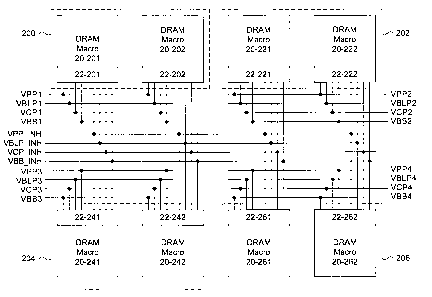
embodiment of the present invention is shown in Figure 4. In the embedded DRAM
system
of Figure 4, there are eight embedded DRAM macro's 20 organized into four
groupings 200,
202, 204 and 206. Each grouping 200, 202, 204 and 206 includes two embedded
DRAM
macro's 20. Each embedded DRAM macro 20 has VPP, VBLP, VCP and VBB internal
power supplies in their respective internal power supply circuit areas 22.
Grouping 200
includes DRAM macro's 20-201 and 20-202 having internal power supply circuit
areas 22-
201 and 22-202, respectively. Grouping 202 includes DRAM macro's 20-221 and 20-
222
having internal power supply circuit areas 22-221 and 22-222, respectively.
Grouping 204
includes DRAM macro's 20-241 and 20-242 having internal power supply circuit
areas 22-
6
CA 02541046 2006-03-27
241 and 22-242, respectively. Grouping 206 includes DRAM macro's 20-261 and 20-
262
having internal power supply circuit areas 22-261 and 22-262, respectively. As
shown in
Figure 4, each grouping shares one common set of bi-directional voltage test
lines. For
example, grouping 200 has VPP1, VBLP1, VCP1 and VBB1 voltage test lines. A
common
set of power control signals, VPP_INH, VBLP_INH, VCP_INH and VBB_INH are
connected to each internal power supply. Hence during testing, any one or more
of the same
internal power supplies in all the embedded DRAM macro's 20 can be disabled in
parallel by
activating the corresponding power control signal(s). An advantage of the
common power
control signal testing architecture of Figure 4 is that all embedded DRAM
macro's 20 can be
tested in parallel.
Therefore, the common power control signal testing architecture of Figure 4
only
requires sixteen voltage test lines and four power control signals with
corresponding test
pads, for a total of twenty test pads. This number is far less than the worst-
case scenario of
sixty-four test pads.
In a situation where ACV can affect the output voltages, such as in advanced
process
technologies, even groupings of two adjacent embedded DRAM macro's 20 can have
different output voltages. Hence, it may be desirable to test the output
voltages of each
embedded DRAM macro 20 in order to obtain finer control and tuning of the
power supplies
of each embedded DRAM macro 20. Therefore within each grouping, only the
internal power
supplies of one embedded DRAM macro 20 are enabled, while the internal power
supplies of
the other embedded DRAlV1 macro's of the group are disabled. Accordingly, for
each
grouping, there is preferably a corresponding set of power control signals
dedicated for
disabling the internal power supplies of each embedded DRAM macro 20. With
reference to
Figure 3, such a control scheme would have up to "n" sets of "m" power control
signals
V_CTRL, expressed as V_CTRL[l:n][l:m]. This embodiment can be referred to as
the
selective power control signal testing architecture.
An example implementation of the selective power control signal testing
architecture
embodiment of the present invention is shown in Figure 5. In the embedded DRAM
system
of Figure 5, there are eight embedded DRAM macro's 20 organized into four
groupings 300,
302, 304 and 306. Each grouping 300, 302, 304 and 306 includes two embedded
DRAM
macro's 20. Each embedded DRAM macro 20 has VPP, VBLP, VCP and VBB internal
power supplies in their respective internal power supply circuit areas 22.
Grouping 300
7
CA 02541046 2006-03-27
includes DRAM macro's 20-301 and 20-302 having internal power supply circuit
areas 22-
301 and 22-302, respectively. Grouping 302 includes DRAM macro's 20-321 and 20-
322
having internal power supply circuit areas 22-321 and 22-322, respectively.
Grouping 304
includes DRAM macro's 20-341 and 20-342 having internal power supply circuit
areas 22-
341 and 22-342, respectively. Grouping 306 includes DRAM macro's 20-361 and 20-
362
having internal power supply circuit areas 22-361 and 22-362, respectively. As
shown in
Figure 5, each grouping shares one common set of bi-directional voltage test
lines, which is
identical to the configuration shown for the implementation of Figure 4. With
two embedded
DRAM macro's 20 per grouping, two sets of power control signals are required.
As shown in
Figure 5, power control signals VPP_INH1, VBLP_INH1, VCP_INHI and VBB_INH1 are
connected to the first embedded DRAM macro 20 in each grouping, while
VPP_INH2,
VBLP INH2, VCP INH2 and VBB INH2 are connected to the second embedded DRAM
macro 20 in each grouping. During testing, any one or more of the same
internal power
supplies in either of the embedded DRAM macro's 20 of each group can be
disabled in
parallel. Therefore, exactly one internal power supply has dedicated use of
the shared voltage
test line.
The advantage of the selective power control signal testing architecture of
Figure 5 is
that the internal power supplies of individual embedded DRAM macro's 20 can be
tested.
Since one embedded DRAM macro 20 of each group can have dedicated use of its
common
voltage test lines, four embedded DRAM macro's 20 can be tested in parallel.
The remaining
four embedded DRAM macro's 20 would be tested in a following test cycle. For
example, in
a first test cycle VPP_INH2, VBLP_INH2, VCP_INH2 and VBB_INH2 can be activated
to
disable the corresponding internal power supplies of the second embedded DRAM
macro's
20 in each grouping. For example, the left side embedded DRAM macro's 20 in
each
grouping can provide their internal voltages onto the shared voltage test
lines. In a following
test cycle, VPP_INH1, VBLP_INH1, VCP_INHI and VBB_INH1 can be activated to
disable
the corresponding internal power supplies of the first embedded DRAM macro's
20 in each
grouping. Hence the right side embedded DRAM macro's 20 in each grouping can
provide
their internal voltages onto the shared voltage test lines.
Although the selective power control signal testing architecture of Figure 5
requires a
total of twenty-four test pads, this architecture provides high testing
flexibility. For example,
the selective power control signal testing architecture of Figure 5 can be
controlled to operate
8
CA 02541046 2006-03-27
in the same manner as the common control signal testing architecture of Figure
4. This can be
done simply by driving the two sets of power control signals with the same
signals, such that
there is effectively one set of logical power control signals. For example,
VPP_INH2 would
be the same as VPP_INH1.
It has been previously described that the internal power supplies of one
embedded
DRAlV1 macro 20 of each grouping can have dedicated access to the common
voltage test
lines. In an alternate control scheme, different internal power supplies from
different
embedded DRAM macro's 20 of each grouping can be tested at the same time. Take
a
situation where VPP_INH1, VCP_INH1, VBLP_INH2 and VBB_INH2 are activated to
disable the internal power supplies they are connected to. The left side
embedded DRAM
macro 20 has its VPP and VCP power supplies disabled, giving the right side
embedded
DRAM macro 20 dedicated access to the VPP1 and VCPI lines. The right side
embedded
DRAM macro 20 has its VBLP and VBB power supplies disabled, giving the left
side
embedded DRAM macro dedicated access to the VBLPI and VBBI lines. Those of
skill in
the art will understand that different combinations can be obtained.
The previously described embodiments of Figures 4 and 5 illustrate embedded
DRAM macro groupings where the same internal power supply (ie. VPP power
supply) in a
grouping share the same voltage test line (ie. VPPI). In an alternate
embodiment, each
embedded DRAM macro can have all its internal power supplies connected to one
common
voltage test line. This embodiment can be referred to as the common voltage
test line testing
architecture.
Figure 6 shows an example implementation of the common voltage test line
testing
architecture. The embedded DRAM system of Figure 6 is similar to the ones
previously
shown in Figures 4 and 5. Eight embedded DRAM macro's 20 are organized into
four
groupings 400, 402, 404 and 406. In the present example, the VPP, VBLP, VCP
and VBB
internal power supplies of each embedded DRAM macro 20 of one group are
connected to
respective common voltage test lines. Grouping 400 includes DRAM macro's 20-
401 and 20-
402 having internal power supply circuit areas 22-401 and 22-402,
respectively. Grouping
402 includes DRAM macro's 20-421 and 20-422 having internal power supply
circuit areas
22-421 and 22-422, respectively. Grouping 404 includes DRAM macro's 20-441 and
20-422
having internal power supply circuit areas 22-441 and 22-442, respectively.
Grouping 406
9
CA 02541046 2006-03-27
includes DRAM macro's 20-461 and 20-462 having internal power supply circuit
areas 20-
461 and 22-462, respectively.
As shown in Figure 6, the left side embedded DRAM macro 20 has all its
internal
power supply outputs connected to V_Linel, while the right side embedded DRAM
macro 20
has all its internal power supply outputs connected to V_Line 2. In
otherwords, each
embedded DRAM macro 20 of each grouping has a dedicated voltage test line. A
common
set of power control signals VPP_INH, VCP_INH, VBLP_INH and VBB_INH are
connected
to the respective internal power supplies of all the embedded DRAM macro's 20,
which is the
same configuration as shown for the embodiment of Figure 4. In the presently
shown
embodiment, only one internal power supply of each embedded DRAM macro 20 can
be
tested in parallel. For example, to test the VPP power supplies, VCP_INH,
VBLP_INH and
VBB_INH would be activated to disable those corresponding internal power
supplies of all
the embedded DRAM macro's 20. In this particular embodiment, only 12 test pads
are
required.
It is noted that the output of each internal power supply is directly
connected to the
respective internal power supplies. Therefore, without further modifications,
having all the
outputs simply connected to each other via the voltage test line will result
in a situation where
all the internal power supplies are physically shorted together during normal
operation.
Accordingly, the presently shown embodiment of Figure 6 will require isolation
means in line
between the internal power supply and its connection to the voltage test line
(ie. V_Linel),
for isolating the internal power supply from the voltage test line. In
otherwords, the isolation
means functions as a 4:1 multiplexor implemented with gating transistors,
controllable by
additional selection signals. In combination with the power control signals,
any combination
of internal power supplies and gating transistors can be turned on or off. If
required, the
control signals can be set to higher/lower than normal voltage levels for
overdriving the
gating transistors. Implementations of such a modification should be well
known to those
skilled in the art.
Those of skill in the art will appreciate that further embodiments can be
obtained by
combining the previously illustrated and described test architecture
embodiments. For
example, the common voltage test line testing architecture of Figure 6 can
have all the
internal power supplies in a grouping connected to one voltage test line, but
two sets of
CA 02541046 2006-03-27
power control signals can be used to control the internal power supplies of
each embedded
DRAM macro 20 in the groupings.
The previously described embodiments of the invention use embedded DRAM
macros as sub-systems. However, any type of integrated sub-system can be used.
Furthermore, a combination of different types of sub-systems can be grouped
together,
instead of the same type of sub-system.
The above-described embodiments of the present invention are intended to be
examples only. Alterations, modifications and variations may be effected to
the particular
embodiments by those of skill in the art without departing from the scope of
the invention,
which is defined solely by the claims appended hereto.
11