Note: Descriptions are shown in the official language in which they were submitted.
CA 02542518 2006-04-12
WO 2005/038048 PCT/CN2004/001180
APPARATUS AND METHODS FOR
DETECTING NUCLEIC ACID IN BIOLOGICAL SAMPLES
FIELD OF THE INVENTION
This invention relates to apparatus and methods for detecting nucleic acid in
biological samples. In particular the present invention relates to a novel
apparatus and method
for detecting DNA sequences using, field-assisted nucleic acid hybridization
and to methods
for optimizing the performance of such apparatus, and further the present
invention extends
to the use of field-assisted hybridization in any biological process that
includes charged
entities.
BACKGROUND OF THE INVENTION
The emergence of high-density polynucleotide (eg DNA or RNA) array technology
has transformed the basic concepts of genomics and protemics analysis. The
transition from
"dot blots" to "arrays on glass slides" and then to DNA microarrays (also
known as DNA
chips) has revolutionised the industry by making large-scale clinical
diagnostic testing and
screening processes realistic for practical applications. As 'is well-known, a
typical
microarray, with reactive sites in a predetermined configuration on a
substrate, will exhibit a
binding pattern when exposed to a sample with target nucleic acid fragments
having a base
sequence complementary to that of the capture fragments attached on the
reactive sites. The
binding pattern and the .binding efficiency can be detected by optical or
electronic methods
when an appropriate detection mechanism is used, which may include for example
fluorescent labeling, current detection or impedance measurement..
The use of electrically-assisted nucleic acid hybridization is a known
technique in the
analysis of biological samples containing DNA, e.g. blood, plasma, urine etc.
Conventionally,
a chip for DNA detection is formed from one of a variety of materials
including glass, silica
and metal. On the surface of the chip a number of electrical contacts are
formed using known
1
CA 02542518 2006-04-12
WO 2005/038048 PCT/CN2004/001180
techniques. To detect a particular DNA sequence in a biological sample,
capture probes
consisting of complementary DNA fragments are attached to the chip surface by
means of an
attachment layer which is conventionally an agarose gel. If a biological
sample contains the
target DNA, the target DNA will bind to the complementary DNA fragments by
hybridization, and various imaging techniques may be used to detect such
hybridization and
= thus the presence in the sample of the target DNA.
PRIOR ART
Nucleic acid fragments are electrically charged and thus can be attracted
towards a
particular site by electrostatic attraction by the use of electrodes and thus
by the application
of an appropriate electrical current the hybridization process may be
accelerated and thus the
detection process is also accelerated. However, it is not possible to use the
electrode in direct
contact with the nucleic acid fragments because of the danger of
electrochemical degradation
or electrolysis of the sample. Conventionally therefore a
permeation/attachment layer is
normally coated on the electrode as shown in US 5605662 and 6306348.. The
penneation/attachment layer is normally made from porous materials, eg sol-gel
materials,
porous hydrogel materials, porous oxides and serves to allow the selective
diffusion of small
ions and also as an attachment surface for the capture probes. Direct contact
of the nucleic
acid fragments with the electrode is reduced owing to the size of the pores of
the porous
materials which are generally too small to allow the larger nucleic acid
fragments to pass
through.
When a voltage is applied to the electrode underneath the
permeation/attachment
-layer, the devices- of the prior art can provide electrophoretic transport
effects without
electrochemical degradation of the sample and can thus enhance hybridization.
However,
such prior techniques for enabling electrically-induced hybridization are not
without their
drawbacks. For example, porous materials such as hydrogels and polymers are
vulnerable to
2
CA 02542518 2006-04-12
WO 2005/038048 PCT/CN2004/001180
deterioration under contact with aqueous solutions, various chemicals and a
number of
ambient factors. The preparation of sol-gel materials are costly and
complicated, increasing
the manufacturing costs. Furthermore the porous materials are naturally
fragile and
susceptible to adsorption and the trapping of undesired foreign materials such
as moisture
hydrocarbons in air, resulting in a shorter-shelf-life of the devices.
SUMMARY OF THE INVENTION
According to the present invention there is provided apparatus for detecting
target
nucleic acid in a sample, comprising a substrate formed with at least one
reaction cell,
wherein said reaction cell includes an attachment surface formed of a
dielectric material for
the attachment of nucleic acid capture probes, and wherein a metal electrode
is provided in
direct contact with said dielectric material. The sample may comprise
biological substances
and the sample may be wastewater, solution or reagent. The sample may also be
a biological
-- sample such as blood, plasma 'or urine.
Preferably the electrode is provided beneath the attachment surface, that is
to say in
contact with a side of the dielectric material opposite from the attachment
surface.
Conceivably, however, it could be applied in contact with a side of the
dielectric material or
even in contact with the attachment surface itself.
In preferred embodiments of the invention the dielectric material is
preferably an
oxide, for example it may be selected from the group consisting of A1203, Si02
and Ta205.
The metal electrode for example may be formed of aluminum.
In preferred embodiments of the invention the apparatus may comprise a
multilayer
structure comprising a first base layer, a second insulating layer formed on
said base layer, a
third layer formed on said insulating layer and comprising patterned
conductive regions
defining at least one metal electrode, and a fourth layer comprising at least
one region of
3
CA 02542518 2006-04-12
WO 2005/038048 PCT/CN2004/001180
dielectric material, wherein each said metal electrode in said third layer is
covered by a
region of dielectric material in said fourth layer. Preferably the patterned
conductive regions
of the third layer are separated by regions formed of dielectric material.
Still more preferably
the regions of dielectric material in said fourth layer are separated by
regions of a passivation
material, and the regions of passivation material may extend over the edges of
said regions of
dielectric material to define said reaction cells.
Viewed from another broad aspect the present invention provides a method of
performing field-assisted hybridization in the detection of nucleic acid
targets from a
biological sample, comprising the steps of providing a reaction cell having an
attachment
surface formed of a dielectric material, providing a metal electrode beneath
in direct contact
with said dielectric material, attaching nucleic acid capture probes to said
attachment surface,
adding a sample to said reaction cell, and providing an electrical potential
to said electrode.
The sample may comprise biological substances and the sample may be
wastewater, solution
or reagent. The sample may also be a biological sample such as blood plasma or
urine.
The electrical potential may be applied as a continuous potential, or may be a
smoothly varying, or pulsed potential.
Viewed from another broad aspect the present invention also provides a method
of
attracting or repelling electrically-charged entities to or from a surface of
a reaction cell when
performing a biological reaction, comprising the steps of providing a
dielectric material as
said surface, and generating an electrical field by inducing charge-separation
in said dielectric
material. The electrically charged entities may be nucleic acid molecules.
Viewed from a still further aspect the invention also extends to a method of
forming
an array of reaction cells for performing biological analysis, comprising the
steps of
patterning metal electrodes on an insulating substrate, depositing regions of
dielectric
4
CA 02542518 2010-10-29
material on said metal electrodes, and forming a rim around the edges of
Lipper surfaces of
said regions of dielectric material so as to define said reaction cells.
Preferably, for example, the method may comprise depositing a layer of metal
on an
insulating surface, covering a desired pattern of said metal layer with a
photoiesist and
removing the remainder of said metal layer by an etching process, depositing a
layer of said
dielectric material over said pattamed metal whereby said dielectric material
covers said
patterned metal and occupies the areas between said patterned electrodes,
depositing a
passivation layer over said layer of dielectric material, pattering said
passivation layer with a
photoresist and removing said passivation layer to open said dielectric
material where it
covers said metal electrodes to define reaction said cells.
According to one aspect of the present invention, there is provided an
apparatus for
detecting target nucleic acid in a sample, comprising a substrate formed with
at least one
reaction cell, wherein said reaction cell includes a layer formed of a
dielectric material
defining an attachment surface, for the attachment of nucleic acid capture
probes, and
wherein a metal electrode is provided in direct contact with said dielectric
attachment layer,
wherein said dielectric attachment layer is structured such that applying an
electrical potential
to said metal electrode causes a charge separation in said dielectric
attachment layer without
generating a flow of electric current or causing transfer of electrons between
said dielectric
attachment layer and a sample in said reaction cell.
According to another aspect of the present invention, there is provided an
apparatus for
detecting target biological material in a sample, comprising a substrate
formed with at least
one reaction cell, wherein said reaction cell includes a surface formed of a
dielectric material,
wherein a metal electrode is provided in direct contact with said dielectric
material, and
wherein said dielectric material is structured such that applying an
electrical potential to said
metal electrode can cause a charge separation in said dielectric material
without generating a
flow of electric current or causing transfer of electrons between said
electrode and a sample
in contact with said dielectric material.
According to still another aspect of the present invention, there is provided
a method
of performing field-assisted hybridization in the detection of a nucleic acid
target from a
sample, said method comprising:
CA 02542518 2010-10-29
(i) providing a reaction cell having a layer formed of a dielectric material
defining an
attachment surface;
(ii) providing a metal electrode in direct contact with the dielectric
attachment layer;
(iii) attaching nucleic acid capture probes to said dielectric attachment
layer;
(iv) adding the sample to said reaction cell; and
(v) providing an electrical potential to said metal electrode causing charge
separation in said
dielectric attachment layer but without generating a flow of electric current
or causing
transfer of electrons between said layer and the sample.
According to yet another aspect of the present invention, there is provided a
method
of attracting or repelling electrically-charged entities to or from a surface
of a reaction cell
when performing a biological reaction of a sample, said method comprising:
(i) providing a layer formed of a dielectric material defining said surface;
and
(ii) generating an electrical field by inducing charge-separation in said
dielectric layer but
without generating a flow of electric current or causing transfer of electrons
between said
dielectric layer and the sample.
According to a further aspect of the present invention, there is provided a
method of
accelerating a detection process for a biological molecule performed in a
reaction cell, said
method comprising:
(i) providing a layer formed of a dielectric material defining an attachment
surface of said
reaction cell; and
(ii) generating an electrical field by inducing charge-separation in said
dielectric material but
without generating a flow of electric current or causing transfer of electrons
between said
dielectric layer and the biological molecules or medium in which the
biological molecules
reside.
According to yet a further aspect of the present invention, there is provided
a method
of forming an array of reaction cells for performing biological analysis, said
method
comprising:
(i)patterning metal electrodes on an insulating substrate;
(ii) depositing regions of dielectric material on said metal electrodes; and
(iii) forming a rim around the edges of upper surfaces of said regions of
dielectric material so
as to define said reaction cells;
5a
CA 02542518 2010-10-29
wherein said dielectric material is deposited such that applying an electrical
potential to said
metal electrodes can cause a charge separation in said dielectric material
without generating a
flow of electric current or causing transfer of electrons between said
electrodes and a sample
in said reaction cells.
BRIEF DESCRIPTION OF THE DRAWINGS
Some embodiments of the invention will now be described by way of example and
- wvifh reference to the accompanying drawings, in which: -
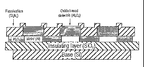
Fig.l is a sectional view through a chip in accordance with an embodiment of
the
present inventio;o'
Fig.2 is a view similar to Fig.1 but showing the chip in use,
Xig.3 is a -schematic illustration showing the underlying principle of
preferred
embodiments of the present invention,
Fig.4 illustrates the steps in a possible fabrication process,
Figs. 5(a) and (b) show first test results with a sample target oligomers of
synthetic (3-
actin (91 bases pure) and an hybridization time of 90 minutes. Panel (a) shows
results
obtained with the addition of target oligomers when no potential is applied to
the Al
electrode. Panel (b) shows results without addition of target oligomers when
no
potential is applied to the Al electrode.
Figs. 6(a) and (b) show second test results with a sample target oligomers of
synthetic
(3-actin (91 bases pure) and an hybridization time of 10 minutes. Panel (a)
shows
results obtained with the addition of target oligomers when a potential of +10
V is
applied to the Al electrode. Panel (b) shows results obtained without addition
of
target oligomers when no potential of +10 V is applied to the Al electrode.
Figs. 7(a), (b) and (c) show third test results with a real sample target
oligomers of
AIV H5 subtype (250 bases, mixed with other non-specific oligomers) and an
hybridization time of 10 minutes. Panel (a) shows results obtained with the
addition
of target oligomers when a potential of +10 V is applied to the Al electrode.
Panel (b)
5b
CA 02542518 2010-10-29
shows results obtained without addition of target oligomers when a potential
of +10 V
is applied to the Al electrode. Panel (c) shows results obtained with addition
of target
oligorners when no potential is applied to the Al electrode.
DETA I ED DESCRIPTION OF PREFERRED EMBODIMENTS
5c
CA 02542518 2006-04-12
WO 2005/038048 PCT/CN2004/001180
Fig.1 shows in section a part of an embodiment of the present invention that
includes
three cells for receiving a sample-containing buffer solution, but it will be
understood that
any number of cells could be provided, and they would normally be formed in a
rectangular
array.
The device according to an embodiment of the invention is fabricated by
sequential
deposition onto a silicon substrate using conventional deposition techniques.
Firstly,
(Fig.4(a)) an insulating layer formed of Si02 of a thickness of between about
200nm to
500nm is formed on the Si substrate by any suitable technique including
thermal oxidation or
by any suitable deposition technique such as for example sputtering,. electron
beam
evaporation and the like. On top of the insulating layer is formed (Fig.4(b))
a layer of
aluminum of a thickness of between about 500nm to 1000nm again using any
conventional
deposition techniques.
Once the layer of aluminum has been formed, it is patterned (Fig.4(c)) using a
layer of
photoresist and the unmasked areas are removed by etching (Fig.4(d)) and the
photoresist is
removed (Fig.4(e)). The chip is then coated (Fig.4(f)) with A1203 to a
thickness of between
50-500nm with regions of A1203 being formed between the aluminum regions that
are formed
on the silicon dioxide substrate. A passivation layer of (for example) Si3N4
is then deposited
(Fig.4(g)) on the A1203 by means of plasma enhanced chemical vapor deposition.
or similar
techniques. The passivation layer is then patterned with a photoresist
(Fig.4(h)) and the
passivation layer is then etched (Fig.4(i)) to open up the A1203 areas that
are to become the
attachment surfaces of the reaction cell. Finally the photoresist is removed
(Fig.4(j)).
The result of this fabrication process is the multi-layer structure of Fig. 1.
Regions of
aluminum are formed on the insulating layer of silicon dioxide and these
aluminum regions
are separated by A12O3. Formed on top of the layer of aluminum and A12O3 is a
layer that
comprises regions of A12O3 located above the regions of aluminum and separated
from each
6
CA 02542518 2006-04-12
WO 2005/038048 PCT/CN2004/001180
other by the passivation material Si3N4 which covers the A1203 regions
separating the
aluminum regions on the lower later. The passivation material also extends to
cover the edges
of the top A1203 so as to define a surface for a biological sample to be
placed for analysis.
It will thus be understood that in the example shown in Fig. 1 the chip is
formed with
three cells 1 - 3 each formed of A1203 with an underlying pad of aluminum.
Although not
shown in Fig.1 when the aluminum regions are formed by etching, electrical
connections may
also be formed that allow an electrical potential to be applied to the
aluminum regions.
Once the chip of Fig. 1 has been fabricated it can be used as the basis for a
number of
different biological tests and assays. In particular each cell 1 - 3 in Fig. 1
may be provided
with suitable capture probes as shown in Fig.2. Depending on the tests to be
performed, each,
cell may be provided with the same capture probes or with different capture
probes, the
capture probes having nuclei acid fragments that are complementary to
fragments in the
sample that the test. or assay is looking for. In the example of Fig.2, the
cells 1- 3 are all
identical and a drop of sample containing buffer solution is added to the cell
so that it covers
all three cells.
As will be understood by those skilled in the art, if the sample contains
fragments of
nucleic acid that are complementary to the capture probes, they will bind to
the capture
probes by the process of hybridization and this may be detected by known
techniques. Since
the nucleic acid fragments are electrically charged, this hybridization can be
enhanced by
providing an electrical field that will attract desired nucleic acid fragments
towards the
attachment surface and the capture probes. The mechanism by which this may be
done is
shown in Fig: 3.
In particular, as shown in Fig.3, if a potential is applied to the aluminum
electrode
underlying a cell, then because A1203 is a dielectric material charge
separation will occur
within the A1203 the polarity of which will depend on the polarity of the
voltage applied to
7
CA 02542518 2006-04-12
WO 2005/038048 PCT/CN2004/001180
the aluminum electrode beneath the A1203. As shown on the left of Fig.3, if a
positive
potential is applied to the aluminum electrode, then the upper surface of the
A1203 will also
have a positive potential which would attract negatively . charged fragments,
and repel
positively charged fragments. Conversely, if a negative potential is applied
to the aluminum
electrode, then the upper surface of the A1203 will also have a negative
potential which would
attract positively charged fragments, and repel negatively charged fragments
as shown in the
right-hand side of Fig.3. Thus selectively applying an electrical potential to
the aluminum
electrodes that are directly underneath and in direct contact with the A1203
attachment surface
enables the selective attraction/repelling of nucleic acid fragments and thus
enables
electrically-induced hybridization. It should be understood that the potential
can be applied in
many different ways. The potential could for example be a constant continuous
potential,
may be smoothly varying, or may be pulsed either with regular pulses or in any
desired
pattern.
A particular advantage of the present invention, at least in its preferred
forms, in
contrast with the prior art is that undesired electrochemical reactions and/or
electrolysis can
be completely avoided since there is no electron transfer between the sample
solution and the
surface of the dielectric layer. The nucleic acid fragments can thus be
electrically drawn to
the attachment surface without electrochemical degradation. A further
important advantage of
the field-assisted hybridization method and apparatus of the present
invention, at least in
preferred forms, is that the salt concentration and pH value of the sample
will not be changed.
These parameters are crucial factors influencing the hybridization efficiency
and the stability
of the hybridized nucleic acid fragments. Prior art electrically-assisted
hybridization
techniques lead to significant changes in the salt concentration and the pH
due to
electrochemical reactions and other techniques, such as special buffer
solutions, are required
in order to compensate for these effects. A further advantage of the present
invention is that
8
CA 02542518 2006-04-12
WO 2005/038048 PCT/CN2004/001180
no electrochemical reactions will occur and in turn this will mean that the
solutions/reagents
involved in the detection process will not be disturbed. There will be no
bubble formation
and/or precipitation during the detection process, which is important in
improving the quality
of the detected signal.
It should also be understood that while preferred embodiments of the present
invention are described in the context of accelerated hybridization in the
detection of nucleic
acid fragments, the invention is more generally applicable to any biological
process that
involves electrically-charged entities and where it is desired to be able to
control the
movement of such electrically-charged entities by attracting or repelling such
entities to or
from a surface.
Figs.5 to 7 show a number of experimental results using the-structure of
Figs.1 to 3
with and without an electrical potential applied to the aluminum electrodes
beneath the cells.
It will of course be understood that in all of these examples the reaction
times, applied
voltages and other parameters are purely exemplary and may be varied as
desired.
Figs.5(a) and (b) show a control in which in neither case is an electrical
potential
applied to the aluminum electrodes and therefore the hybridization proceeds
without
electrical assistance. In this Example the target oligomers in the sample are
synthetic (3-actin
(91 bases, pure) and the hybridization time is 90 minutes. The target
oligomers are present in
the sample of Fig.5(a) and not present in the sample of Fig.5(b). In neither
Fig.5(a) or 5(b) is
an electrical potential applied to the aluminum electrode, but the cells are
clearly darker in
Fig.5(a) than 5(b) owing to the presence of the target oligomers in the sample
of Fig.5(a).
In Figs.6(a) and (b) the conditions are the same as in Fig.5(a) and (b) in
that the same
target oligomers are provided in the sample of Fig.6(a) and no target
oligomers are provided
in the sample of Fig.6(b). In this example, however, a potential of +10V is
applied to the
aluminum electrodes and the hybridization time is reduced to 10 minutes. A
comparison of
9
CA 02542518 2006-04-12
WO 2005/038048 PCT/CN2004/001180
Figs.5(a) and 6(a) shows that in Fig.6(a) the cells are much darker clearly
illustrating even
though the hybridization time has been substantially reduced, demonstrating
the effectiveness
of the applied voltage in accelerating the hybridization. The similarity.
between Figs.5(b) and
6(b) where no target oligomers are present shows that the applied voltage does
not lead to any
false positive results.
Fig.7(a)-(c) illustrate a third example in- which the target oligomers in the
sample are
avarian influenza virus (AIV). H5 subtype (250 bases mixed with other non-
specific
oligomers). In all three cases (a)-(c) the hybridization time is 10 minutes.
The differences
between Figs.7(a)-(c) are as follows: In Fig.7(a) target oligomers are present
in the sample
and an electrical potential of +10V is applied to the aluminum electrodes
beneath the cells; In
Fig.7(b) no target oligomers are present in the sample and an electrical
potential of +1OV is
applied to the aluminum electrodes beneath the cells; and in Fig.7(c) target
oligomers are
present in the sample but no electrical potential is applied to the aluminum
electrodes beneath
the cells. Again this example shows that with a hybridization tithe of only 10
minutes, the
application of a +10V potential to the electrode results in accelerated
hybridization and strong
signal (very dark areas in the cells of Fig.7(a)). In comparison the
similarity in appearance
between Figs.7(b) (without target and with applied potential) and Fig.7(c)
(with target but
without applied potential) shows that it is not possible to obtain effective
hybridization in the
same time period (10 minutes) without electrically assisted hybridization.
The present invention at least in its applied forms provides a simple low-cost
device
that allows nucleic acid field-assisted hybridization and/or other biological
processes to
proceed at a much faster rate with high performance that can be applied to a
large number of
possible applications. The present invention employs the principle of charge-
separation in a
dielectric material that is in contact with an electrode to which a potential
is applied. In the
embodiments described above the electrode is aluminum and the dielectric
material is Al203,
CA 02542518 2006-04-12
WO 2005/038048 PCT/CN2004/001180
but other combinations of metal electrode and dielectric attachment surface
are also possible.
For example, Si02, Ta205 may be used as oxide based dielectric materials for
the attachment
surface.
In contrast with the prior art devices that use a permeation layer, the oxide
based
dielectric layer in direct contact with the electrode provides a structure
that is robust,
compact, chemically inert towards most of the acids, alkalis and other
reagents commonly
used in biological reactions. The structure is also stable with regards to
ambient factors such
as temperature and humidity and is less vulnerable to physical damage. The
production costs
are lower and the device can be manufactured very easily using standard
deposition
techniques and other microelectronics fabrication techniques. Indeed the use
of such
microelectronics deposition and fabrication techniques in the manufacture of
the devices of
the present invention also has the advantage that the- devices can readily be
incorporated into
.other devices made using the same or similar technology.
11