Language selection

Search

Patent 2543736 Summary

Third-party information liability

Some of the information on this Web page has been provided by external sources. The Government of Canada is not responsible for the accuracy, reliability or currency of the information supplied by external sources. Users wishing to rely upon this information should consult directly with the source of the information. Content provided by external sources is not subject to official languages, privacy and accessibility requirements.

Claims and Abstract availability

Any discrepancies in the text and image of the Claims and Abstract are due to differing posting times. Text of the Claims and Abstract are posted:

  • At the time the application is open to public inspection;
  • At the time of issue of the patent (grant).
(12) Patent Application: (11) CA 2543736
(54) English Title: METHOD AND DEVICE FOR SECURE, INSULATED AND ELECTRICALLY CONDUCTIVE ASSEMBLING OF TREATED SEMICONDUCTOR WAFERS
(54) French Title: PROCEDE ET DISPOSITIF POUR ASSEMBLER SOLIDEMENT, DE MANIERE ISOLANTE ET ELECTROCONDUCTRICE, DES PLAQUETTES DE SEMICONDUCTEURS TRAITEES
Status: Deemed Abandoned and Beyond the Period of Reinstatement - Pending Response to Notice of Disregarded Communication
Bibliographic Data
(51) International Patent Classification (IPC):
  • B81B 7/00 (2006.01)
(72) Inventors :
  • KNECHTEL, ROY (Germany)
(73) Owners :
  • X-FAB SEMICONDUCTOR FOUNDRIES AG
(71) Applicants :
  • X-FAB SEMICONDUCTOR FOUNDRIES AG (Germany)
(74) Agent: GOWLING WLG (CANADA) LLP
(74) Associate agent:
(45) Issued:
(86) PCT Filing Date: 2004-10-29
(87) Open to Public Inspection: 2005-05-12
Availability of licence: N/A
Dedicated to the Public: N/A
(25) Language of filing: English

Patent Cooperation Treaty (PCT): Yes
(86) PCT Filing Number: PCT/DE2004/002413
(87) International Publication Number: WO 2005042401
(85) National Entry: 2006-04-26

(30) Application Priority Data:
Application No. Country/Territory Date
103 50 460.5 (Germany) 2003-10-29

Abstracts

English Abstract


The invention concerns a method and a device for assembling treated
semiconductor wafers (1, 2), for obtaining not only a secure assembly, but an
electrical connection (5) between the semiconductor wafers or between the
electronic structures (3) comprising the latter as well. The invention is
characterized in that the secure assembly is produced by means of structured
intermediate glass layers (6; 6a), with low melting point, acting as
insulating layers, and the electrical connection is produced by means of an
electroconductive sealing glass (5).


French Abstract

L'invention concerne un procédé et un dispositif pour assembler des plaquettes de semiconducteurs traitées (1,2), permettant de réaliser non seulement un assemblage solide, mais aussi une connexion électrique (5) entre les plaquettes de semiconducteur ou entre les structures électroniques (3) comportant ces dernières. Selon l'invention, l'assemblage solide est réalisé au moyen de couches intermédiaires en verre (6; 6a), structurées, à bas point de fusion, servant de couches isolantes, et la connexion électrique est réalisée au moyen d'un verre de scellement électroconducteur (5).

Claims

Note: Claims are shown in the official language in which they were submitted.


9
We claim:
1. ~A process for the firm connection of processed semiconductor wafers,
preferably
for connecting system wafers (1) supporting microelectromechanical or
electronic
structures with cover wafers (2), which, preferably also support electronic
structures, wherein, in the case of more than two wafers, the waters located
in a
central area of the stack are in particular simultaneously both system wafer
and
cover wafer, wherein in an operation of a mechanically firm connecting both
electrically insulating connections (6, 6a, 6b) and electrically conductive
connections
(5) are produced between the semiconductor wafers, said process comprising at
least the following specific main operations
- applying structured layers of electrically non-conducting and electrically~
conducting glass paste on respectively one of the two wafer sides to be
connected with each other;
- conditioning and premelting of the glasses or glass pastes (5, 6);
- geometrical alignment of the wafers to be connected;
- joining, in particular bonding, of the wafers at a processing temperature of
the
glasses or glass pastes using mechanical pressure.
2. ~The process according to claim 1, characterized in that the glass pastes,
in
particular glass solders are applied with a screen printing process.
3. ~The process according to claim 1, characterized in that the non-
conducting, low-
melting glass paste and the electrically conducting glass paste have different
conditioning and premelting conditions and that, consequently, the
conditioning and~
premelting are implemented successively in a respectively separate process.

10
4. The process according to claim 1, characterized in that the non-conducting,
low-
melting glass paste and the electrically conducting glass paste have
substantially
the same processing temperature.
5. The process according to claim 1, characterized in that the non-conducting,
low-
melting glass paste and the electrically conducting glass paste have different
processing temperatures and these are successively passed in a process.
6. The process according to claim 1 and any of claims 2 to 5, characterized in
that at
least one of the wafers is electrically connected in an area that is not
structured
electronically (area of the starting material).
7. The process according to claim 1 and any of claims 2 to 6, characterized in
that the
wafers are electrically connected at specific switching points in their
electronically
structured areas (3).
8. The process according to claim 1 and any of the subsequent claims,
characterized
in that the formation of the connections of the glass pastes takes place at a
temperature of less than 450°C.
9. The process according to claim 1 and any of the subsequent claims,
characterized
in that the electric connection of the substrate for SOI wafers is implemented
through previously produced openings in a buried oxide layer and in an active
silicon layer, in particular the wall areas of the opening in the active
silicon layer
being provided with an insulating layer (7a) prior to the electric connection.
10. Wafer arrangement which was produced or can be produced according to the
process according to claim 1 or a process of the subsequent claims.

11
11. A process for the firm connection of processed semiconductor wafers,
preferably
for connecting a system wafer (1) supporting microelectromechanical or
electronic
structures with a cover wafer (2) which, in particular also supports
electronic
structures, wherein in an operation of a mechanically firm connecting both
electrically insulating connections and electrically conductive connections
are
produced between the semiconductor wafers, said process comprising at least
the
following specific main operations
- applying a first electrically non-conducting, structured layer and a second
electrically conducting layer of respectively one glass paste (5, 6) on at
least one
of the two wafer (1, 2) to be connected with each other;
- conditioning of the glass pastes (5, 6);
- premelting of the conditioned glass pastes (5, 6);
- geometrical alignment of the wafers (1, 2) to be connected;
- joining, in particular bonding, of the wafers (1, 2) at a processing
temperature of
the glass pastes using mechanical pressure.
12. The process according to claim 11, wherein the glass pastes (5, 6), in
particular
glass solders, are applied with a screen printing process.
13. The process according to claim 11, wherein the non-conducting, low-melting
glass
paste (6, 6a) and the electrically conducting glass paste (5) have different
conditioning and/or premelting conditions and that, consequently, the
conditioning
and premelting of each of the pastes are implemented successively in a
respectively separate process.
14. The process according to claim 11, wherein the non-conducting, low-melting
glass
paste (5) and the electrically conducting glass paste (6) have substantially
the same
processing temperature.

12
15. The process according to claim 11, wherein the non-conducting, low-melting
glass
paste (5) and the electrically conducting glass paste (6) have different
processing
temperatures and these are successively passed in a process.
16. The process according to claim 11, wherein at least one of the wafers is
electrically
connected in an area not structured electronically (area of the starting
material).
17. The process according to claim 11, wherein at least one of the wafers is
electrically
connected at specific switching points in their electronically structured
area(s) (3).
18. The process according to claim 11 and any of the subsequent claims,
wherein the
formation of the connections of the glass pastes takes place at a temperature
of
less than 450°C.
19. The process according to claim 11 and any of the subsequent claims,
wherein the
electric connection of a substrate (11) of an SOI wafer (8) is implemented
through at
least one previously produced opening in a buried oxide layer (10) and in an
active
silicon layer (9), in particular the wall areas of the opening in the active
silicon layer
being provided with an insulating layer (7a) prior to the electric connection
(5) with
the conducting glass solder.

13
20. A process for the firm connection of processed semiconductor wafers,
preferably
for connecting system wafers (1) supporting microelectromechanical or
electronic
structures (3) with cover wafers (2) which may also support electronic
structures,
wherein in the case of more than two wafers the wafers located in a central
area of
the stack are simultaneously both system wafer and cover wafer, wherein in an
operation of a mechanically firm connecting both electrically insulating
connections
and electrically conducting connections are produced between the semiconductor
wafers, characterized by the following specific main operations
- applying structured layers of electrically non-conducting and electrically
conducting glass pastes on respectively one of the two wafer sides to be
connected with each other;
- conditioning and premelting of the glasses (5, 6);
- geometrical alignment of the wafers to be connected;
- joining (bonding) of the wafers at the processing temperature of the glasses
using mechanical pressure.

Description

Note: Descriptions are shown in the official language in which they were submitted.


Roy Knechtel, et al. CA 02543736 2006-04-26 Translation of PCT/DE2004/002413
as filed
1
METHOD AND DEVICE FOR SECURE, INSULATED AND ELECTRICALLY
CONDUCTIVE ASSEMBLING OF TREATED SEMICONDUCTOR WAFERS
The invention relates to a process for connecting processed semiconductor
wafers by
means of electrically conducting and electrically insulated, structured
intermediate
connecting layers. A wafer arrangement that can be produced with the process
is also
involved.
The connecting of processed semiconductor wafers is used in the manufacture of
microelectronic and microelectromechanical systems in order to cover specific
structures
already during the wafer process by a cap. On the one hand, this operation is
necessary
in order to protect sensitive mechanical structures during subsequent
processing steps
and/or to implement the actual encapsulation of the individual elements, e.g.
optical
components, already during wafer bonding and to thus make special structures
possible.
Customary processes for connecting e.g. system and cover wafers are anodic and
direct
bonding and bonding by means of low-melting intermediate glass layers (glass
frit
bonding).
As a rule, the mechanically and/or electrically active elements are located on
the system
wafer. Whereas the cover layer mostly only serves as a covering protection
(cap) and
does not have any electrical structures or only has a few electrical
structures according to
the prior art.
The aforementioned bonding processes have the property that the wafers are not
conductingly connected with each other. On the one hand, this is due to the
fact that the
cover wafer itself is not conducting (anodic bonding). On the other hand,
intermediate
layers formed during bonding are not conducting (binding oxide during direct
bonding,
intermediate glass layer during glass frit bonding). When using the
encapsulation bonding
it is, however, mostly necessary to specifically connect the entire cover
and/or structures
on the cover in an electrically conducting fashion. An electric connection of
the entire
cover is partly necessary in order to connect it to a specific potential, e.g.
mass.

Roy Knechtel, et al. cz~ 02543736 2006-04-26 Translation of PCT/DE2004/002413
as filed
2
For the reading of capacitive sensors evaluation electrodes are required on
the cover
which must have a contact towards the system wafer in order to make a wire
bonding
during the setting up and connection processes in one plane possible.
To increase the packing density of microsystems it is also advantageous to
integrate
evaluation circuits on the cover wafer, if they can have an electric contact
towards the
system wafer. So far, electric wafer-to-wafer contacts have only been known so
far from
anodic bonding. Here, metallization areas of the wafers to be connected are
brought into
mechanical contact and are firmly pressed together due to the resultant wafer
connection
force, cf. KADAR et al., Sensors & Actuators A52 (1996), pages 151 to 155 -
Aluminium
press-on contacts for glass to silicon anodic bonding.
This process is not completely convincing. On the one hand, the areas of
electric contact
interfere with the formation of the actual wafer bond connection. On the other
hand, there
is no material connection in the area of the electric contacts so that their
reliability is thus
doubtful. The glass frit bonding is considered to be the wafer bonding process
for
encapsulation purposes that can be used most universally , since it renders
very high
bonding yields and since, due to the planarizing effect of the molten
intermediate glass
layer, it balances surface profiles of the wafers to be connected and, thus,
makes lateral
metallic contact leadthroughs in the bonding interface possible.
The invention is based on the technical object of designing a connection
process in such
a way that a firm connection that tightly seals with respect to cavities of at
least two
semiconductor wafers is provided with a simultaneous electric connection of
the wafers.
The object is attained with claims 1, 11 or 10 or 20 (as a process and a
product).

Roy Knechtel, et al. cz~ 02543736 2006-04-26 Translation of PCT/DE2004/002413
as filed
3
the combination of conducting and insulating glass structures specifically
reaches areas
of the cover wafer during glass frit bonding so that they are electrically
connected.
The invention is especially suited for microelectromechanical structures which
are
integrated with structures of the evaluation electronics. Moreover, more than
two
semiconductor wafers can also be connected with each other as a stack. Then,
there are
also central areas in this stack, where cover wafer and system wafer may be
present at
the same time.
The invention is explained and supplemented by means of examples with two
semiconductor wafers using the drawing.
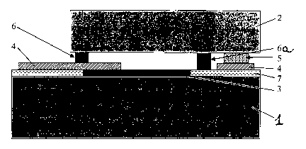
Fig. 1 is a system wafer 1 which was connected with a cover wafer 2 according
to an
example of a process, namely as a schematic section along line/plane A-A of
Fig. 2.
Fig. 2 is a top view of an arrangement as it is shown in Fig. 1.
Fig. 3 is a variant of a conducting connection between system wafer and cover
wafer.
Fig. 3' is a further variant of a conducting connection between system wafer
and cover
wafer analogously to Fig. 3.
As it is shown in Fig. 1, low-melting, structured insulating intermediate
glass layers 6, 6a,
6b and the electrically conductive solder 5 on the basis of glass (glass
paste) connect the
system wafer 1 with the cover wafer 2, a selective contacting of the cover
wafer 2 with the
~ Translator's note: should read "Fig. 4"

Roy Knechtel, et al. cz~ 02543736 2006-04-26 Translation of PCT/DE2004l002413
as filed
4
system wafer 1 and/or between electrically active structures 3 of both wafers
being
established at the same time (as a product and/or as a process).
As regards the process, the application and the premelting of both glass
solders 6, 5 can
be implemented separately and successively. Here, the application and
premelting of the
first glass solder 6 (as a structured layer) is implemented and, separately
and, after a
certain time interval has expired, the application and premelting of the
second glass
solder 5 is implemented.
However, an application that takes place successively and a joint premelting
are
possible, in particular in the temperature range of 450°C.
A conditioning of the glass pastes in the customary extent and the customary
processes
in semiconductor technology take place prior to a premelting.
The conducting and non-conducting wafer connections are e.g. formed at the
same time
in the bonding process. For this, the processing temperatures of both used
glasses are in
the same range.
Metallic strip conductors 4 which are located on the system wafer 1 and are
insulated
with respect to the substrate by means of an intermediate insulator 7 can be
embedded
in the area of the non-conducting glass solder. This makes the low-impedance
connection of the structures 3 that are to be protected with the cover 2
possible. At the
same time, the structures that must be covered by the cover can be packed in a
hermetically tight fashion.
The wafer connection 6, 6a, 6b which is mainly mechanically supporting can be
implemented by means of a glass solder. As regards it thermal expansion it
adapts very

Roy Knechtel, et al. CA 02543736 2006-04-26 Translation of PCT/DE2004/002413
as filed
good to silicon. The electric contact surfaces must be kept small in order to
minimize
mechanical stresses.
In the top view of Fig. 2 the sectional line A is plotted which, provided with
a step results
in the sectional view of Fig. 1. The cover 2 as the cover wafer is only shown
symbolically,
actually removed, in Fig. 2, in order to be able to have a look at the
structures located
beneath it. The wafer 2 is provided with a checked pattern, is unequivocally
allocated to
Fig. 1 as regards its marginal areas and covers the structure 3 to be
protected, but
reveals, at the same time, the hermetic sealing and the mechanical support by
the
isolator layer (the structured layer 6a, 5b, 6) which is set up in a frame-
shaped fashion.
The bonding islands and the strip conductors 4 can also be reocognized in this
picture
outside and below the cover wafer 2.
If SOI wafers 8 (silicon on insulator) are used as system wafers as is shown
in Fig. 3,
there is the possibility to electrically connect substrate 11 of the SOI wafer
by means of
the conducting glass solder 5. For this purpose, the active layer 9 of the SOI
substrate
and the buried oxide 10 must be opened at the corresponding site so that the
electrically
conducting glass solder 5 can flow into the opening and thus contact the
carrier wafer
In order to connect only one or the desired points of the active semiconductor
layer 9, the
semiconductor layer 9 is insulated at the perforated walls. An intermediate
insulator 7, cf.
Fig. 1, is not shown in Fig. 3. Since the current SOI-based technologies
include these
partial steps, there is no extra expenditure.
In a variant to Fig. 3, which was already described there implicitly, but
which is completely
shown in Fig. 4, the intermediate insulator 7a is defined as regards its area
within the
opening occupied by the conducting glass solder 5, which, however, does not
penetrate
up to the semiconductor layer 9 so that it contacts it, since an in particular
cylindrical
insulator layer 7a is provided which, resting on the top of the semiconductor
layer 9, may

Roy Knechtel, et al. cz~ 02543736 2006-04-26 Translation of PCT/DE2004/002413
as filed
6
still have a circumferential edge in a round, cornered or difFerently shaped
fashion. The
strip conductor 4 is only provided above this edge and the semiconductor layer
9.
Moreover, the design according to Fig. 4 is designed in the same way as that
in Fig. 3 so
that reference is made to the description thereof.
If the corresponding electric contact areas and the necessary wafer connection
frames
are taken into consideration in the design of system wafer 1 and cover wafer
2, the
following process for producing the electrically conducting and insulating
wafer
connections is e.g, possible:
screen printing for applying the electrically non-conducting glass paste 6 on
the
cover wafer 2;
conditioning and premelting of the electrically non-conducting glass paste 6;
screen printing for applying the electrically conducting glass paste 5 on the
cover
wafer,
conditioning and premelting of the electrically conducting glass paste;
aligning of system and cover wafers;
bonding under mechanical pressure at the processing temperature of the glasses
and/or glass pastes 5, 6.
Alternatively the application of the glasses and/or glass pastes may also be
carried out in
the reverse order and/or on the system wafer 1 with correspondingly adapted
further
process steps as shown above.

Roy Knechtel, et al. cz~ 02543736 2006-04-26 Translation of PCTJDE2004J002413
as filed
7
List of reference numerals
1 System wafer with microelectromechanical and/or electronic structures 3
2 Cover wafer, in particular also provided with electronic structures
3 Microelectromechanical and/or electronic structures to be protected
4 Metal structures, feed fines and bonding islands (bonding pads)
Electrically conductive connecting glass (first glass paste, structured)
6 Electrically insulating connecting glass {second glass paste, structured)
7 Intermediate insulating layer
8 SOI wafer (silicon on insulator)
9 Silicon layer (active layer) supporting active electronic structures
7a Insulation in the opening of the active layer
Buried oxide of the SOI wafer
11 Supporting wafer (substrate)
12 Insulating ducts in the active layer 9

Representative Drawing
A single figure which represents the drawing illustrating the invention.
Administrative Status

2024-08-01:As part of the Next Generation Patents (NGP) transition, the Canadian Patents Database (CPD) now contains a more detailed Event History, which replicates the Event Log of our new back-office solution.

Please note that "Inactive:" events refers to events no longer in use in our new back-office solution.

For a clearer understanding of the status of the application/patent presented on this page, the site Disclaimer , as well as the definitions for Patent , Event History , Maintenance Fee  and Payment History  should be consulted.

Event History

Description Date
Application Not Reinstated by Deadline 2010-10-29
Time Limit for Reversal Expired 2010-10-29
Inactive: Abandon-RFE+Late fee unpaid-Correspondence sent 2009-10-29
Deemed Abandoned - Failure to Respond to Maintenance Fee Notice 2009-10-29
Letter Sent 2006-09-15
Inactive: Single transfer 2006-08-01
Inactive: Cover page published 2006-07-10
Inactive: Courtesy letter - Evidence 2006-07-04
Inactive: Notice - National entry - No RFE 2006-06-29
Application Received - PCT 2006-05-24
National Entry Requirements Determined Compliant 2006-04-26
Application Published (Open to Public Inspection) 2005-05-12

Abandonment History

Abandonment Date Reason Reinstatement Date
2009-10-29

Maintenance Fee

The last payment was received on 2008-10-02

Note : If the full payment has not been received on or before the date indicated, a further fee may be required which may be one of the following

  • the reinstatement fee;
  • the late payment fee; or
  • additional fee to reverse deemed expiry.

Please refer to the CIPO Patent Fees web page to see all current fee amounts.

Fee History

Fee Type Anniversary Year Due Date Paid Date
Basic national fee - standard 2006-04-26
Registration of a document 2006-08-01
MF (application, 2nd anniv.) - standard 02 2006-10-30 2006-10-11
MF (application, 3rd anniv.) - standard 03 2007-10-29 2007-10-09
MF (application, 4th anniv.) - standard 04 2008-10-29 2008-10-02
Owners on Record

Note: Records showing the ownership history in alphabetical order.

Current Owners on Record
X-FAB SEMICONDUCTOR FOUNDRIES AG
Past Owners on Record
ROY KNECHTEL
Past Owners that do not appear in the "Owners on Record" listing will appear in other documentation within the application.
Documents

To view selected files, please enter reCAPTCHA code :


To view images, click a link in the Document Description column. To download the documents, select one or more checkboxes in the first column and then click the "Download Selected in PDF format (Zip Archive)" or the "Download Selected as Single PDF" button.

List of published and non-published patent-specific documents on the CPD .

If you have any difficulty accessing content, you can call the Client Service Centre at 1-866-997-1936 or send them an e-mail at CIPO Client Service Centre.


Document
Description 
Date
(yyyy-mm-dd) 
Number of pages   Size of Image (KB) 
Claims 2006-04-26 5 169
Abstract 2006-04-26 1 15
Description 2006-04-26 7 261
Drawings 2006-04-26 2 308
Representative drawing 2006-04-26 1 60
Cover Page 2006-07-10 1 93
Reminder of maintenance fee due 2006-07-04 1 110
Notice of National Entry 2006-06-29 1 192
Courtesy - Certificate of registration (related document(s)) 2006-09-15 1 105
Reminder - Request for Examination 2009-06-30 1 116
Courtesy - Abandonment Letter (Maintenance Fee) 2009-12-24 1 174
Courtesy - Abandonment Letter (Request for Examination) 2010-02-04 1 165
PCT 2006-04-26 6 257
Correspondence 2006-06-29 1 29
Fees 2006-10-11 3 134
Fees 2007-10-09 3 145
Fees 2008-10-02 3 161