Note: Descriptions are shown in the official language in which they were submitted.
CA 02544758 2006-05-03
WO 2005/048676 PCT/US2004/033492
DUAL STAGE PRE-HEATER
TECHNICAL FIELD
The present invention relates in genexal to electronic component process
assembly and
re-work systems, and in particular to pre-heating systems for use when
soldering or de-soldering
electronic components on printed circuit boards.
BACKGROUND OF THE INVENTION
Electronic components are attached to printed circuit boards (PCBs) by
soldered
connections. When attaching or detaching electronic components, the solder
connection to the
PCB is heated to a temperature at which solder reflow occurs. However,
performing a proper
solder reflow operation is a much more complex task than simply heating up the
solder to its
reflow temperature. Tlus is due to the fact that the temperature profile of
the solder needs to be
maintained within an appropriate narrow process window that changes over time.
In other
words, the temperature of the solder connecting the electronic component to
the PCB must be
maintained within an appropriate narrow temperature range, with this narrow
temperature range
being varied over time to achieve proper solder reflow conditions. Moreover,
there are
temperature considerations when dealing with the electronic component and the
circuit board
itself. For example, excess temperature differentials' through the electronic
component may tend
to damage the electronic component. Damage can also be caused by simply
subjecting the
electronic component to excessively high temperatures for an extended period
of time. It is also
necessary to avoid excessive temperature differentials across the PCB to avoid
causing warpage
of the PCB itself. As such, there are numerous reasons that the working
temperature ranges of
the solder, the electronic component and the PCB must all be maintained within
clearly defined
limits.
During a typical assembly or re-work operation, the temperature of the solder
is typically
increased in a series of controlled steps or stages, with each stage
accomplishing a particular
function in the overall soldering reflow process. The first stage is simply
applying a low
temperature "preheat". This preheating stage removes any excess moisture from
the PCB and
the electronic component. Next, the temperature of the PCBA is raised during a
"soalc" stage at
which time the temperature of the PCB is substantially equalized. Next, the
temperature is
raised during a "ramp" stage (resulting in rapid heating of the soldered
connection, and
activation of flux). Thereafter, the temperature is briefly stepped up to the
actual "reflow"
temperature stage. A cool down stage follows quickly thereafter.
CA 02544758 2006-05-03
WO 2005/048676 PCT/US2004/033492
During this process, it is important that the duration of time at which the
solder
temperature is actually in its "reflow" stage is not too long. This is due to
the fact that such high
temperatures (especially if prolonged) may tend to damage the electronic
component itself. As a
result, it is desired to raise the solder temperature just high enough to
cause reflow, but only for
a short period of time. As can be seen, the overall soldering reflow process
necessitates
operating within narrow temperature windows over time.
The above discussed problems are even more complicated when using today's lead-
free
solders. This is principally due to the fact that lead free solders have
lugher reflow temperatures.
Therefore, it is necessary to heat lead-free solders to higher temperatures to
achieve reflow. Yet,
it is still important that maximum temperatures (or temperature differentials)
are not exceeded so
that PCB becomes warped. Consequently, working with lead-free solders requires
operating
within a much tighter temperature profile windows and thus, a much tighter
temperature
management and control system is required.
Various systems have been devised to provide heating to the solder connecting
the
electronic component to the PCB. Unfortunately, these existing systems all
tend to suffer from
various disadvantages.
A first type of system is a simple forced air convection system. Examples of
such forced
air convection systems include Summit 1100 made by SRT, Inc. of Connecticut.
In such
systems, a pre-heater is positioned below the PCB to direct heated air upwards
against the
bottom of the PCB, thereby raising the temperature of the PCB above ambient
temperature. A
forced air convection heater in the tool head is then used to heat the
electronic component from
above. The bulk of the heat supplied to the solder is actually supplied from
above (i.e. from the
heater in the tool head). It is this heat from above that actually causes the
solder to reflow.
Unfortunately, these types of systems have disadvantages. For example,
problems exist
when the forced air convection pre-heater is either too large or too small (as
compared to the
PCB positioned thereabove). Specifically, if the pre-heater is too large, the
system will be very
thermally inefficient, since a large portion of the heat is simply lost around
the sides of the PCB.
Moreover, it is very uncomfortable for an operator to work with such a system
since the heat is
simply directed upwards into the operator's face and hands. Conversely, if the
pre-heater is too
small, most of the thermal output will be focused at the center of the PCB.
This causes the PCB
to have an uneven temperature profile thereacross (i.e.: in its X- and Y-
axes). Such non-uniform
temperatures across the PCB may tend to cause the PCB to warp or to deform.
Since the same
pre-heater is used to work on different sized electronic components and on
different PCB's, the
CA 02544758 2006-05-03
WO 2005/048676 PCT/US2004/033492
operator is constantly attempting to deal with the problem of the pre-heater
being either too large
or too small for the job at hand.
A second type of system uses infa-red heating of the PCB. Examples of such
infra-red
heating systems include the 936A system made by Fonton Ins. of Taiwan. Infa-
Red heating has
its own particular disadvantages. For example, it is slow in controlling
temperature changes.
This makes it especially difficult to achieve a desired temperature profile,
especially when
handling lead-free solders which demand narrow temperature windows during
their various
solder reflow heating stages. A fiuther disadvantage of infa-red heating is
that it produces
questionable temperature uniformity in the PGB itself. This is due at least in
part to the fact that
different surfaces of the PCB have different absorption characteristics under
infa-red heating.
Another existing system uses "hot plate" pre-heaters to heat the PCB. Examples
of such
systems include systems made by Airvac Corporation, of Connecticut. Hot plate
heating uses a
heated metal plate that is placed under a PCB assembly to transfer heat
thereto by radiation or
natural convection. Unfortunately, hot plate heading has the disadvantage of
being very slow to
respond to changes in the hot plate set-point temperature. Therefore, it is
slow in controlling
temperature changes. This makes it especially difficult to achieve a desired
solder temperature
profile, especially when handling lead-free solders which demand narrow solder
temperature
windows during their various reflow heating stages.
Legislation requiring lead free solder is becoming mandatory. Unfortunately,
as stated
above, lead-free solders have higher reflow temperatures. However, should the
working
temperatures applied to the electronic components become too high, the
electronic components
may be damaged. As a result, it is necessary to perform component assembly and
re-work
within very narrow temperattue process windows during the various stages of
the solder re-flow
process.
A further disadvantage of all the above discussed systems is that the bulls of
the heating
that actually causes the solder to reflow is the heating that is applied
downwardly from a heater
disposed in the tool head. Thus, the soldered connections (which are found at
the bottom of the
component) are predominantly heated by heat that is applied to the top of the
component (and
conducted downwardly through the component). A disadvantage of this approach
is that large,
unwanted temperature differentials occur in the component's Z-axis.
Specifically, the top of the
component must be raised to a higher temperature than is necessary to cause
the solder to
reflow. The greater the temperature differential through the electronic
component, the greater
the possibility that the component will become damaged.
CA 02544758 2006-05-03
WO 2005/048676 PCT/US2004/033492
What is instead desired is a component assembly and re-work system that
provides a
minimal Z-axis (i.e.: vertical) temperature differential through the
component, while still
providing controllable heating of the solder connection within narrow time and
temperature
parameters. It is further desirable that such a system minimize the X-axis and
Y-axis (i.e.:
horizontal) temperature differentials across the PCB, so as to minimize the
potential for warpage
of the PCB.
As will be explained below, the present invention provides such a system, and
offers
numerous other advantages.
SUMMARY OF THE INVENTION
In preferred aspects, the present invention provides a system for component
assembly
and re-work in which temperature differentials are minimized in each of the X-
, Y- and Z-axes.
This has the advantage of minimizing the potential for damage to the
electronic component or
unwanted changes in either of the electronic component or the PCB to which it
is mounted.
In preferred aspects, the present invention also provides a system which is
able to
generally uniformly heat the PCB to avoid warpage of the board. In addition,
however, the
present invention is also able to apply a focused heating to the PCB at a
location directly under
where the component is mounted to the PCB. As a result, the present invention
provides a
system in which it is possible to provide a low temperature differential
through the electronic
component while maintaining a generally uniform board temperature.
This has the advantage of reducing the amount of top heat that is required
from the heater
in the tool head to cause the solder to reflow. Accordingly, the present
system of focused top
and bottom heating has the advantage of resulting in a lower temperature
differential through the
component in its Z-axis.
As will be shown, the present invention provides a system in which it is
possible to
switch between uniform heating of the underside of the PCB, and focused
heating of the PCB
directly under the electronic component. As will also be shown, preferred
aspects of the present
invention also provide a system which is able to accurately control the
temperature of the solder
connection at the electronic component/ PCB interface within very narrow time
and temperature
parameters.
In preferred embodiments, uniform board heating is achieved with a first stage
of a dual-
stage pre-heater positioned below the PCB. This first stage can be used to
direct air over a large
region (preferably the entire surface) of the bottom of the PCB. The second
stage of this dual-
stage pre-heater can then be used to direct a focused stream of air towards a
localized region of
CA 02544758 2006-05-03
WO 2005/048676 PCT/US2004/033492
the bottom of the PCB directly below the electronic component. The present
invention is,
however, not so limited. For example, during the "pre-heat" and "soak" stages,
the emphasis is
on heating the PCB uniformly. This may be done by only using the first stage,
but also may be
done by using both the first and second stages together. In addition, these
"pre-heat" and "soak"
heating stages may also be accomplished by using the second stage alone (for
example, when
heating a small PCB). When the system enters the "ramp" and "reflow" stages,
focused heat
under the PCBA becomes important. Additional heat may be applied by raising
the temperature,
increasing the air flow or by turning on the second "focused" stage, or a
combination of these
approaches. What the present invention provides is a system that enables all
of these different
heating approaches.
An advantage of applying focused heat on the PCB at a location directly below
the
electronic component is that it reduces the amount of top heat that must be
delivered from the
heater in the tool head to cause the solder to reflow. This has the specific
benefit of reducing the
Z-axis temperature differential through the electronic component itself.
In preferred embodiments, the present invention provides a system for
electronic
component processing, including: ~ a frame configured to hold a PCB; a tool
head connected to
the frame, the tool head being configured to position an electronic component
on top of the
PCB; a heater disposed in the tool head, the heater being configured to direct
heat towards the
electronic component; and a dual-stage pre-heater connected to the frame, the
dual-stage pre-
heater being configured to direct heat towards the PCB in general, and the
electronic component
specifically. Preferably, the dual-stage pre-heater comprises a first stage
configured to generally
uniformly heat the PCB, and a second stage configured to heat a focused region
of the PCB
adjacent to the electronic component. More generally, the dual-stage pre-
heater comprises a
first stage configured distribute heat over a wider area than the second
stage. Thus, the second
stage is configured to apply heat in a more focused region than the first
stage. Both stages may
be operated together, or independently of one another, or at different
intensities. In preferred
embodiments, each of the first and second stages of the dual-stage pre-heaters
are forced air
convection heater systems. The first and second stages of the pre-heater are
preferably both
positioned below the PCB such that the first stage can be used to uniformly
heat the bottom of
the PCB and then the second stage of the pre-heater can be used to apply a
focused heat to the
bottom of the PCB (directly underneath the electronic component positioned
thereon) so as to
assist in causing solder reflow at the electronic component / PCB interface.
CA 02544758 2006-05-03
WO 2005/048676 PCT/US2004/033492
In.preferred aspects, the second stage of the pre-heater can be used to
provide uniform
heat during the first two heating stages (i.e., "pre-heat" and "soak"). During
the final two
heating stages (i.e., "ramp" and "reflow") focused heat can be provided by
changing the system
air flow and / or temperature. In addition, large PCB's may require
simultaneous operation of
the first and second stages of the pre-heater to achieve uniform heating of
the PCB and then
change the heating rate of the second stage of the pre-heater when it is time
for focused heat.
In preferred embodiments, the first and second stages of the dual-stage pre-
heater supply
heated air in flows that are concentric to one another. In optional preferred
embodiments, a
focusing chamber is connected to the output of the second stage of the pre-
heater. The focusing
chamber may be conical shaped. A second stage of the pre-heater that is
moveable with respect
to the first stage of the pre-heater is also contemplated, all keeping within
the scope of the
present invention.
In preferred embodiments, the dual-stage pre-heater further comprises a bowl,
wherein
each of the first and second stages of the pre-heater supply air flow into the
bowl such that air
flows in a vortex in the bowl. The bowl may optionally have two chambers, with
each of the first
and second stages of the pre-heater supplying air flow into one of the two
chambers of the bowl.
The present invention also provides a dual-stage pre-heater for heating a PCB
with an
electronic component positioned thereon, including: a first forced air
convection stage that may
be used to uniformly heat a PCB, and a second forced air convection stage that
may be used to
heat a focused region of the PCB.
The present invention also provides a method of soldering or de-soldering an
electronic
component on a PCB, comprising: positioning an electronic component on top of
a PCB; pre-
heating the bottom of the PCB with a dual-stage pre-heater by: uniformly
heating the bottom of
the PCB with a first stage of the pre-heater, and heating a focused region of
the PCB directly
below the electronic component with the second stage of the pre-heater; and
then heating the top
of the electronic component with a heat source positioned above the electronic
component.
BRIEF DESCRIPTION OF THE DRAWINGS
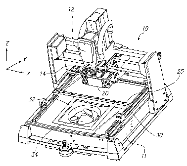
Fig. 1 is a perspective view of an electronic component assembly and re-worlc
platform
incorporating a dual-stage pre-heater in accordance with the present
invention. (The dual-stage
pre-heater is shown in dotted lines as it is located directly below a PCB
supported by the
system.)
CA 02544758 2006-05-03
WO 2005/048676 PCT/US2004/033492
Fig. 2 is a top plan view of a first embodiment of the dual-stage pre-heater.
Fig. 3 is a perspective view of the dual-stage pre-heater of Fig. 2, further
including a
conical shaped focusing chamber connected to the output of the second stage of
the dual-stage
pre-heater.
Fig. 4 is a schematic sectional side elevation view of the invention, showing
its preferred
method of use.
Fig. 5 is a schematic sectional side elevation view of an alternate embodiment
of the
invention.
Fig. 6 is a perspective view of the pre-heater corresponding to the embodiment
of Fig. 2.
Fig. 7 is a perspective view of the pre-heater corresponding to the embodiment
of Fig. 4.
DETAILED DESCRIPTION OF THE DRAWINGS
Fig. 1 shows a perspective view of the present dual-stage pre-heater
invention, as
incorporated into a platform for component assembly or re-work. Figs. 2
through 7 show
various further aspects of the present dual-stage pre-heater invention.
Refernng first to Fig. 1, a system or platform 10 for electronic component
processing is
provided. System 10 includes a frame 11 and a movable tool head 12 which is
selectively
positionable in both the X- and Y-directions. Tool head 12 is used to position
and place an
electronic component 20 onto a printed circuit board (PCB) 25. W preferred
embodiments, tool
head 12 is first moved to a desired position in the X- and Y-directions, such
that electronic
component 20 is positioned directly above the location at which it is to be
soldered to PCB 25
(PCB 25 is also shown in Figs. 4 and 5). Then, a retractable vacuum tube 13 is
extended to
lower electronic component 20 onto PCB 25 (see also Figs. 4 and 5). In
addition, tool head 12
may itself be moved vertically to assist in positioning electronic component
20 onto PCB 25.
Dual-stage pre-heater 30 is incorporated into platform 10 such that it is
positioned below
PCB 25, as shown. It is to be understood that dual-stage pre-heater 30 may be
incorporated into
various soldering assembly or re-work systems, all keeping within the scope of
the present
invention. It is also to be understood that dual-stage pre-heater 30 is by
itself a novel invention
and may be manufactured and sold for use in other existing systems. As such,
the component
platform illustrated as system 10 is merely exemplary.
Further discussion of the operation of exemplary system 10, and its various
preferred
optional features can be found by refernng to co-pending U.S. Patent
Application Serial No.
10/053,512, filed November 2, 2001. As explained therein, an X and Y
positioning system
found in system 10 enables movement of PCB 25 with respect to frame 11.
However, the
CA 02544758 2006-05-03
WO 2005/048676 PCT/US2004/033492
present invention is not so limited. For example, movement of pre-heater 30
with respect to a
stationary PCB 25 is also contemplated within the scope of the present
invention. In either
embodiment, system 10 enables movement of PCB 25 with respect to pre-heater
30. Therefore,
the location at which electronic component 20 is mounted to PCB 25 can easily
be centered
directly above pre-heater 30, thus ensuring that focused heat from pre-heater
30 is delivered to
the underside of PBC 25 directly under electronic component 20. Consequently,
the present
invention provides a system that is flexible enough to cope with a large
variation in PCB sizes.
A heater 14 (or the output from a heat source) is provided in tool head 12.
Heater 14 is
configured to direct heat downwardly towards the top of electronic component
20.
Such heat is illustrated by air flow lines H1 in Figs. 4 and 5. (It is to be
understood that
heater 14 may comprise a heater element and blower system positioned in tool
head 12, or it
may simply comprise an output port of a heating system located elsewhere in
system 10.)
Dual-stage pre-heater 30 is connected to frame 11 with dual-stage pre-heater
30 being
configured to direct heat upwards towards the bottom of PCB 25. Dual-stage pre-
heater 30
comprises a first stage 32 and a second stage 34. First stage 32 and second
stage 34 preferably
both comprise forced air convection heater systems. However, the present
invention xs not so
limited. For example, one or more of stages 32 or 34 could be an infra-red
heater, or any other
type of pre-heater. In such optional embodiments, it is preferred that one
stage provides
generally uniform PCB heating, and the other stage provides focused heating of
electronic
component 20. However, either or both of stage 32 or 34 may be used to provide
heating in
accordance with the preferred systems and methods of the present invention.
Stages 32 and 34
may be operated independently of one another (and at varying intensities) to
during the solder
reflow process.
First stage 32 is configured to generally uniformly heat the bottom (or a
substantial
portion of the bottom) of PCB 25. As such, first stage 32 advantageously
ensures a generally
uniform temperature throughout PCB 25 in the X- and Y-directions. This is
particularly
advantageous in that it decreases the potential for warping of PCB 25. The
heat from first stage
32 is illustrated by air flow lines H2 in Figs. 2, 4 and 5.
Second stage 34 is preferably positioned to supply heated air flow
concentrically within
the heated air flow supplied by first stage 32, as shown. It is to be
understood that although the
entire second stage 34 may itself be physically positioned concentrically
within first stage 32, it
is instead possible that only the output path of the heated air flow supplied
by second stage 34 be
positioned concentrically within the output path of the heated air flow
supplied by first stage 32.
In optional embodiments, second stage 34 may comprise a movable, focused pre-
heater. This
CA 02544758 2006-05-03
WO 2005/048676 PCT/US2004/033492
embodiment may be particularly advantageous in addressing situations where
electronic
component 20 is positioned close to the edge of the PCB. Such an embodiment of
the invention
may make it possible to produce a smaller system.
Second stage 34 is preferably configured to only heat a focused region of PCB
25. Most
preferably, this focused region is the region directly under electronic
component 20. As will be
explained, heater 14 and second stage 34 together advantageously provide
focused heating on
electronic component 20 from above and below, respectively. The heated air
flow from second
stage 34 is illustrated by air flow lines H3 in Figs. 2, 4 and 5.
As seen in Figs. 2 through 6, pre-heater 30 may optionally comprise a bowl 33
with each
of first stage 32 and second stage 34 supplying heated air flow into bowl 33.
As can be seen in
Figs. 2 and 3, the heated air supplied by stages 32 and 34 can be introduced
into bowl 33 such
that the air flows in a vortex in bowl 33. As shown in Fig. 4, bowl 33 may
have two chambers
36 and 38 with each of first and second stages 32 and 34 supplying air flow
into chambers 36
and 38, respectively. It is to be understood that the present invention is not
so limited. For
example, a single chamber can instead be used to receive the heated air
supplied by both stages
32 and 34.
Figs. 3, 5 and 7 show an embodiment of the invention further including an
optional
focusing chamber 35 connected to the output of the second stage 34 of pre-
heater 30. As can be
seen, focusing chamber 35 may simply comprise a cone having an open top end.
Focusing
chamber 35 assists in focusing heated air flow from second stage 34 on the
underside of PCB 25
in a focused region directly under electronic component 20.
As can also be seen schematically in Figs. 4 and 5, each of first and second
stages 32 and
34 may preferably have dedicated heating elements and blower systems 40 and
42, respectively.
Various individual configurations and placements of heating elements and
blowers may be used
for systems 40 and 42. Thus, it is to be understood that systems 40 and 42 are
illustrated only
schematically. Alternate embodiments and placements of these systems are
contemplated, all
keeping within the scope of the present invention.
Most preferably, systems 40 and 42 can be operated independently from one
another
under operator control. As such, stages 32 and 34 (or systems 40 and 42)
preferably each
comprise a dedicated temperature sensor and controller. Thus, each of first
stage 32 and second
stage 34 are preferably independently controllable by an operator. As a
result, it is possible for
an operator to easily switch between heat generation with first and second
stages 32 and 34.
This may be advantageous in conserving system power, or in managing
temperature profiles.
CA 02544758 2006-05-03
WO 2005/048676 PCT/US2004/033492
Fig. 5 shows an optional embodiment of the invention in which second stage 34
of pre-
heater 30 is movably positionable with respect to first stage 32. As
illustrated, second stage 34
may comprise a moveable arm or tube 37 through which heat from system 42 is
directed.
Preferably, such moveable arm or tube is positionable in both of the X- and Y-
directions such
that it may be positioned under various electronic components positioned at
different locations
on PCB 25. Thus, the system of Fig. 5 is particularly advantageous in
directing focused heat to
specific locations on the bottom of PCB 25. As such, this system may be used
instead of (or to
compliment) systems that move PCB 25 with respect to frame 11 (and thus move
PCB 25 with
respect to pre-heater 30).
In preferred aspects of the present invention, the heat (H1) supplied by
heater 14 does
not exceed 60% of the total heat (H1 + H2 + H3) supplied by heater 14, first
stage 32 and second
stage 34. This result can be achieved due to the focused heating (H3) of
electronic component
delivered by second stage 34 from below. Specifically, focused heating from
below (H3)
reduces the amount of top heat (H1) that must be supplied from above (by
heater 14) to cause
15 solder reflow. As a result, the present system advantageously reduces the
temperature
differential through electronic component 20 in its Z-axis. hi contrast, in
preexisting systems,
typically 80% of the total heat required to cause solder reflow is delivered
from above.
The heated output of first stage 32 is especially useful during the early
stages of the
reflow process. Specifically, it is useful in heating PCB 25 to a temperature
at which moisture is
20 dried from electronic component 20 (around 100 degrees C), and to a
temperature at which the
flux is activated (around 150 degrees C). "Flux" is a material added to metal
prior to soldering.
"Activation of the flux" is the heating of this material to a temperature such
that the oxides
present in the material to be soldered are removed such that the solder wets
to the base material.
A further advantage of the present system is that by providing localized
heating of a
particular component 20 on PCB 25, solder reflow is localized to that
component, thus
permitting easy removal and replacement of individual defective components.
In an exemplary aspect, first stage 32 heats PCB 25 to a generally uniform
temperature
just below the component board's solder reflow temperature, for example, in
the range of 180 to
200 degrees Celsius. Second stage 34 then heats a focused area of PCB 25 to
just below the
component board's solder reflow temperature, for example, in the range of 210
to 220 degrees
Celsius. The additional heat supplied by heater 14 then heats the focused area
of PCB 25 it just
above component board's solder reflow temperature, for example, above 230
degrees Celsius.
to
CA 02544758 2006-05-03
WO 2005/048676 PCT/US2004/033492
In one exemplary embodiment constructed by the present inventors, first stage
32
provides an even stream of hot air over an area up to 22 inches square, and
second stage 34
provides an even stream of hot air over an area up to 10 inches square.
The present invention also provides a method of soldering or de-soldering
electronic
component 20 on PCB 25, comprising: positioning electronic component 20 on top
of PCB 25;
pre-heating the bottom of PCB 25 with dual-stage pre-heater 30 by: uniformly
heating the
bottom of PCB 25 with first stage 32 of pre-heater 30, and heating a focused
region of PCB 25
directly below electronic component 20 with second stage 34 of pre-heater 30;
and then heating
the top of electronic component 20 with a heat source 14 positioned above
electronic component
20. Preferably, the solder used is a lead free solder.
The present invention also provides a kit for soldering or de-soldering
electronic
component 20 on PCB 25, comprising the present system for component process re-
work as
described above; and instructions for use setting forth the present method as
described above.
Such instructions for use may be provided in written form, or may be stored
electronically.
11