Note: Descriptions are shown in the official language in which they were submitted.
CA 02545969 2006-05-12
WO 2005/050955 PCT/US2004/037589
TEST ACCESS MATRIX (TAM) PROTECTOR MODULE AND ASSOCIATED
CIRCUITRY FOR A TELECOMMUNICATIONS SYSTEM
CROSS-REFERENCE TO RELATED APPLICATIONS
This application is related to U.S. Provisional Application Serial No.
60/520,053, filed
on November 14, 2003, and entitled "Test Access Matrix (TAM) Protector Module
and
Associated Circuitry for a Telecommunications System", the disclosure of which
is
incorporated herein by reference and on which priority is hereby claimed.
BACKGROUND AND OBJECTS OF THE INVENTION
The nature of Plain Old Telephone Systems (POTS) equipment in the
telecommunications industry is such that a test facility can locate faults in
the local loop
through the Central Office (CO) equipment. Test facilities to locate faults in
the local loop
that affect high data rate systems such as DSL typically need to be located
between the CO
equipment and the local loop. The test facility is switched into the line that
needs to be tested
using what is known as a Test Access Matrix (TAM). The TAM typically switches
one of a
plurality of two wire telecommunications circuits to a two or four wire test
bus.
Connector blocks are typically installed on Main Distribution Frames (MDF) in
the
CO between the CO equipment and the local loop. Some connector blocks include
contacts
for mounting protector modules, which are electrically connected to the
contacts. A TAM
module in accordance with the present invention that can be plugged into the
contacts on
existing blocks on the MDF offers a substantial benefit over a conventional
TAM that
replaces an existing block. Installation cost and system downtime due to
installing a plug in
TAM is reduced when compared to a unit that must be installed by cutting into
the existing
infrastructure or removing existing hardware that was permanently installed
and permanently
installing new hardware.
Other such plug in devices have been proposed, but no such device seen to date
is
robust and compact enough to be considered adequately reliable. This invention
provides a
means to provide the required functionality and reliability for an acceptable
cost to install.
This solution offers the additional advantage of having single twisted pair
count TAM
modules. In the raze event that a module fails, adjacent circuits are not
affected. Multiple
CA 02545969 2006-05-12
WO 2005/050955 PCT/US2004/037589
low twisted pair count magazines (integrating several single pair count TAM
modules) can
also be used, affording a small installation savings but negatively impacting
life cycle cost.
SUMMARY OF THE INVENTION
The present invention is a TAM system that is installed on a single pin, five-
pin or
other type of telephone protector/connector block. The TAM system includes a
plurality of
TAM modules, a motherboard with a preferably integral control matrix and a
controller that
are preferably installed on a connector block. The TAM modules have integrated
relays and
surge protection devices. Additional connections are required to interface
with the
motherboard rather than the standard 5 connections used in typical single
circuit protector
modules. The motherboard is installed between the protector modules and the
connection
field of the block. A controller can be integrated into the motherboard,
installed onto the
block, or remotely located. The control function is designed to facilitate the
connection of
multiple blocks to each other for control purposes using a low wire count bus.
These and other objects, features and advantages of the present invention will
become
apparent from the following detailed description of illustrative embodiments
thereof, which is
to be read in connection with the accompanying drawings.
BRIEF DESCRIPTION OF THE DRAWINGS
Figure 1 is a block diagram of the overall Test Access Matrix (TAM) system of
the
present invention.
Figure 2 is a detailed schematic diagram of the preferred circuit of a TAM
module of
the present invention, forming part of the system shown in Figure 1.
Figure 3A is a detailed schematic diagram of a portion of the TAM module
circuit
shown in Figure 2 in a first test mode.
Figure 3B is a detailed schematic diagram of a portion of the TAM module
circuit
shown in Figure 2 in a second test mode.
Figure 3C is a detailed schematic diagram of a portion of the TAM module
circuit
shown in Figure 2 in a third test mode.
CA 02545969 2006-05-12
WO 2005/050955 PCT/US2004/037589
Figure 3D is a detailed schematic diagram of a portion of the TAM module
circuit
shown in Figure 2 in a fourth test mode.
Figure 4 is a schematic diagram of the circuit of the motherboard control
matrix of the
present invention, forming part of the TAM system shown in Figure 1.
Figure 5 is an exploded isometric view of selected TAM system components of
the
present invention mounted on a standard single pin connector block.
Figure 6 is an exploded isometric view of selected TAM system components of
the
present invention mounted on a standard five pin connector block.
Figure 7A is a detailed schematic diagram of a portion of the TAM module
circuit
having two relays to interface with a two wire test bus and shown in a normal
mode of
operation (i.e., non-test mode).
Figure 7B is a detailed schematic diagram of the two relay TAM module shown in
Figure 7A in a first test mode.
Figure 7C is a detailed schematic diagram of the two relay TAM module shown in
Figure 7A in a second test mode.
Figure 7 D is a detailed schematic diagram of the two relay TAM module shown
in
Figure 7A in a third test mode.
DETAILED DESCRIPTION OF THE PREFERRED EMBODIMENTS
In accordance with one form of the present invention, a Test Access Matrix
(TAM)
system includes a plurality of protected TAM modules 1 (1) through (n). The
modules 1 are
connected to a motherboard (e.g., a printed circuit board) (2) which as is
illustrated by
Figures 5 and 6 is mountable to one side of a connector block, as will be
described in greater
detail. The TAM system of the present invention also includes a control matrix
(3) and a
controller (4), for example, a circuit, which receives a control signal from
the Central Office
(CO) to initiate, for example, a test of the CO equipment or the local loop
(also referred to
herein as the distribution equipment). The controller (4) and the control
matrix (3) each may
be situated on the motherboard (2) of the TAM system, or may be remotely
situated with
respect to the motherboard (2).
CA 02545969 2006-05-12
WO 2005/050955 PCT/US2004/037589
As shown in Figure 1, the controller (4) receives control signals from the CO,
as
mentioned previously, which control signals contain information designating
what telephone
circuit should be tested and the kind of test which is to be performed. The
controller (4) may
be a demultiplexer circuit or a programmable read only memory (PROM), or a
random access
memory (RAM), or even more preferably, a microcontroller or a dual tone multi-
frequency
(DTMF) controller having preferably I/O (input/output) TTL (Transistor
Transistor Logic)
outputs, such as shown in Figure 4 of the drawings, or any other type of
controller circuit
. known to those skilled in the art. The controller (4) provides signals on a
single wire or a bus
to the control matrix (3) which, in turn, provides signals to the selected TAM
modules (1) in
order to test a particular telephone circuit, either on the distribution side
or the equipment
side, or both, and to select the particular test which is to be performed.
As can be seen from Figure 1 of the drawings, each protected TAM module (1) is
connected to a particular telephone circuit and passes through it signals from
and to the local
loop (i.e., the distribution side) and signals from and to the CO (i.e., the
equipment side).
When a particular telephone circuit is selected for testing, the control
matrix (3) activates
relays or other switching circuits in the corresponding TAM module (1) through
(n)
associated with that telephone circuit. Each TAM module (1) through (n) is
connected to a
test bus, and the particular TAM module having relays or switching circuits
that are activated
by the control matrix (3) provides on the test bus test signals that represent
and from which
may be determined the condition of the telephone lines associated therewith,
that is, the lines
from the CO or the local loop, or both. The test bus is provided to the CO
which may then
determine from the signals carried on the test bus if there is a problem with
the lines, the kind
of problem (for example, a short or open circuit), and on which side (i.e:,
the equipment side
or the distribution side) the problem occurs.
The preferred circuit of the TAM module (1) is shown in Figure 2 of the
drawings.
The TAM module preferably includes three relays (5) - (7) and a protector
circuit (8).
Although relays (5) - (7) are shown, it is of course envisioned to be within
the scope of the
present invention to substitute for the relays solid state circuits that
perform the same function
as the relays.
The relays (5) - (7) are shown in Figure 2 as being double pole, single throw
relays.
Double pole, double throw relays, single pole, double throw relays and single
pole, single
throw relays may also be used. The protector circuit l81 which is ~hnWn in
Fimre ~ is a
CA 02545969 2006-05-12
WO 2005/050955 PCT/US2004/037589
partially balanced solid state overvoltage surge suppressor, as is well known
in the art, and
includes three thyristors, two of which are connected in series between the
two distribution
outputs of the module, referenced in Figure 2 by the notation AD and BD, which
are often
referred to as the tip and ring lines, and the other thyristor is connected
between the series
juncture of the first two thyristors and the ground connection. Of course, any
overvoltage/overcurrent protector circuit (8) or components known in the art
may be
employed, as the user requires.
Referring again to Figure 2 of the drawings, two separate contacts of each of
the first
two relays (5) and (6) are connected to the wires of a four wire test bus
which is connected to
other TAM modules and which is routed to the CO so that the signals provided
by the
activated relays may be evaluated by the CO. The first relay (5) has one end
of its coil
connected to a control line, referred to in Figure 2 as the Control E t~t, and
similarly, the
second relay (6) has one end of its coil connected to a Control D test~ The
other ends of the
coils of the first and second relays (5) and (6) are provided to a power bus.
The third relay~(7) of the preferred TAM module (1) has one end of its coil
connected
to another line referred to in Figure 2 as a Control gr~k, and the other end
of its coil connected
to the power bus referred to previously. Accordingly, energization of one or
more of the
Control E tes~, Control 17 test, Control Brew and the power bus lines will
activate one or more of
the three relays (5) - (7).
The equipment circuit telephone lines are provided to the TAM module (1) and
are
referred to in Figure 2 by the notation AE and BE. The two equipment lines are
connected to
two contacts of the third relay (7) and the other two contacts of the first
relay (5). The other
corresponding contacts of the third relay (7) are connected to the other
contacts of the second
relay (6) and to the protection circuit (8) and the output pins or sockets
connectable to the
distribution lines, referred to in Figure 2 as AD and BD.
The TAM module (1) is shown in Figure 2 in its normal, non-test mode. The
third
relay (7) is energized so that the equipment signals on lines AE and BE pass
through the
contacts of the relay respectively to distribution lines AD and BD, which are
protected by the
protector circuit (8). The first relay (5) and the second relay (6) are not
activated and,
therefore, neither the equipment lines AE and BE nor the distribution lines AD
and BD are
connected to the four wire test bus.
CA 02545969 2006-05-12
WO 2005/050955 PCT/US2004/037589
Figures 3A through 3D show the activated states of the relays in the TAM
protector
module (1) in four different test modes. The activated states of the relays
(5) - (7) can be
configured to perform testing as required, including the monitor or sniff
mode, as shown in
Figure 3A; the break toward equipment mode, as shown in Figure 3B; the break
toward
distribution mode, as shown in Figure 3C; and the make before break split
mode, as shown in
Figure 3D.
More specifically, in the monitor or sniff mode (Figure 7A), relays (5) and
(7) are
activated to close its contacts while relay (6) is not activated and its
contacts remain open so
that the equipment lines are connected to the distribution or local loop while
the lines are
being monitored on two wires of the preferably four wire test bus.
In the break toward equipment mode (Figure 7B), relay (7) deactivates to open
its
contacts, so that the signal from the equipment does not pass through the TAM
module to the
distribution lines, and the first relay (5) is activated to close its contacts
so that the equipment
lines axe connected to two wires of the preferably four wire test bus in order
to monitor the
signal from the Central Office (CO). Relay (6) is deactivated and it contacts
remain open.
In the break toward distribution mode (Figure 7C), again the third relay (7)
is
deactivated so that its contacts are open, thus breaking the connection
between the equipment
lines and the distribution lines, and the second relay (6) is activated to
close its contacts so
that two wires of the preferably four wire test bus are connected to the local
loop (distribution
lines). In this mode, the first relay (5) is deactivated so that its contacts
are open.
In the make before break split mode (Figure 3D), the third relay (7) is
deactivated so
that its contacts open, thus breaking the connection between the equipment and
the local loop,
and the first relay (5) and the second relay (6) are activated to close their
respective contacts,
so that two wires of the four wire test bus are connected to the equipment
lines, and the other
two wires of the four wire test bus are connected to the distribution lines.
The control matrix (3), which is preferably situated on the motherboard (2) is
shown
in Figure 4 of the drawings. The control matrix (3) is preferably a circuit
which employs
drive switches, such as transistors, that activate the relays (5) - (7) in the
TAM modules (1)
through (n). Any number of TTL or microprocessor based control circuits known
in the art
can be used to perform the control function of the control matrix (3). Because
of the need to
direct only one circuit passing through a TAM module (1) to the test bus at
one time, the
CA 02545969 2006-05-12
WO 2005/050955 PCT/US2004/037589
control matrix (3) can be used to minimize the connections from the controller
(4) to the
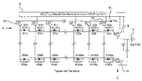
motherboard (2). The control matrix (3) shown in Figure 4 is for a 100 wire
pair TAM
system. Each of the 300 relays shown (Kla through K100c) is in the TAM
modules. For
example, relays Kla, Klb, and Klc are in TAM module No. 1. Relay Kna is shown
by
reference number (5) in Figure 2, relay Knb is shown as reference number (6)
in Figure 2,
and relay Knc is designated by reference number (7) in Figure 2. Protection
diodes Dla,
Dlb, Dlc through D100c are connected in parallel with the relay coils of
relays Kla, Klb,
Kl c through K100c with a normally non-conductive polarity to prevent damage
to the control
matrix (3) due to high voltage spikes caused when the relay coils are switched
off, as is well
known in the art.
The control circuit (13) of the controller (4) sends signals to the switches
of the
control matrix (3). In the case of the control matrix (3) shown in Figure 4,
the switches are
transistors Q1 through Q35. The control circuit (13) that generates the I/O
signals which
control the states of switches (transistors) Ql through Q35 is located in the
controller (4).
Switches/transistors Q1 through Q35 may be located on the motherboard (2) or
in the
controller (4). For the 100 wire TAM system, one to three switches
(transistors) in each row
R of the control matrix (3) (transistor Q1 (14) through transistor Q15 (15)
comprise the first
row) can be activated to provide relay coil voltage (16), also referred to as
Vcc, to a column
of modules. Similarly, one switch in the column C of switches (transistor Q16
(1 ~) to
transistor Q35 (19) comprise one column) can be activated to provide the
signal ground (17)
to a row ofmodules. The relays (5) - (7) in the TAM module (1) at the row R
and column C
intersection will be activated. The combination and sequence of relays
activated will cause
the activated TAM module (1) - (n) to allow the test bus to test the chosen
circuit in one of
the four test configurations shown in Figures 3A - 3D.
Figure 5 illustrates the TAM system of the present invention installed on a
standard
single pin connector block (having one socket for receiving the ground pin of
the protector
module, and four upstanding pins for the equipment lines and the distribution
lines, which are
received by sockets in the respective protector or TAM module). The connector
block (20)
shown has the motherboard (21 ) on the connection field side of the connector
block (20) over
the pins (22) in the block for the distribution and equipment line
connections. The
motherboard (21) preferably does not make electrical contact with the pins
(22) on the block.
Thus, the motherboard (21) may have pass-through holes formed through the
thickness
CA 02545969 2006-05-12
WO 2005/050955 PCT/US2004/037589
thereof which are aligned with and receive the pins (22) of the connector
block (20), the pass-
through holes being insulated from the rest of the circuit on the motherboard
(21). The
equipment and distribution connections within the module (23) make a direct
electrical
connection to the pins (22) on the connector block (20). The control and test
bus connections
of the TAM module (23) are made through a connector (30) mounted on the module
that
connects to a respective connector (25) of a plurality of connectors situated
on the
motherboard (21). The module ground pin (24) for the protector circuit (8)
with the TAM
module (23) makes an electrical connection to the connector block ground.
In Figure 5, three TAM modules (23) are shown, two of which have their
housings
removed to show the inside of the module. One of the modules (23a) is shown
with the first
relay (5), the second relay (6) and the third relay (7). The other module
(23b) with the
housing removed shows an embodiment in which only the first relay (5) or the
second relay
(6), and the third relay (7), are used in the module. One of the first and
second relays (5) and
(6) may be omitted, if fewer test modes are desired. It should be noted that
with only two
relays, additional space is afforded in the TAM module for the circuitry, or
the module may
be made smaller. It should further be noted that the relays (5) - (7) may be
turned on their
side within the module to afford additional space, or all three relays (5) -
(7) may be arranged
in single plane on a printed circuit board within the module.
Figure 6 illustrates the TAM system of the present invention installed on a
standard
five pin connector block (26). The connector block (26) shown in Figure 6 has
the
motherboard (27) installed on the connection side over the block (26). The
distribution and
equipment connections on the connector block (26) are the sockets (28). The
motherboard
(27) preferably does not make electrical contact with the sockets on the block
(28) or the
distribution and equipment pins and ground pins (29) extending from the TAM
module. As
in the previous embodiment shown in Figure 5, the motherboard (27) may include
pass-
through holes (35) formed through the thickness thereof, which holes (35)
receive the
distribution and equipment pins (29) and ground pin (31) of the module. The
equipment and
distribution connection pins (29) protruding from the module (23) make a
direct electrical
connection to the sockets (28) on the connector block. (26) through the pass-
through holes
(35) of the motherboard (27). The TAM modules (23) in both the embodiment
shown in
Figure 5 and the embodiment shown in Figure 6 include a connector (30) for the
control and
test bus connections of the module. This connector (30) mates with a
cooperating connector
CA 02545969 2006-05-12
WO 2005/050955 PCT/US2004/037589
(25) of a plurality of cooperating connectors situated on the motherboard (27)
and disposed in
alignment with the connectors (30) of the TAM modules (23). Thus, the control
and test bus
connections of the module make a direct connection to the motherboard (27).
The module
ground pin (31 ) for the protector circuit makes an electrical connection to
the connector block
ground socket (32) through a respective pass-through hole (35) of the
motherboard (27).
Figures 7A through 7D illustrate a TAM module circuit designed in accordance
with
the present invention to interface with a two wire test bus. Only two relays
(40) and (41) are
required. The designations "nc" and "no" in Figures 7A through 7D respectively
refer to the
"normally closed" and "normally open" position of the contacts of the relays
(40) and (41)
for the TAM module circuit interfacing with a two wire test bus. Each
respective equipment
line is connected to a respective normally open contact of relay (40). The two
distribution
lines are connected to respective switching contacts of relay (41 ). The
normally closed and
normally open contacts of each switching circuit of relay (40) are connected
to the normally
open and normally closed contacts, respectively, of each corresponding
switching circuit of
relay (41). The two wire test bus lines are connected to the switching
contacts of relay (40).
More specifically, Figure 7A shows the normal mode of operation for the TAM
module circuit for the two wire test bus embodiment. Each equipment line is
directly
connected to a respective distribution line, and the test bus lines are not
connected with either
the equipment lines or the distribution lines. Each switching circuit of each
of relays (40) and
(41) is in its normally closed state so that the equipment lines are
electrically connected
through relay (41 ) to the distribution lines.
Figure 7B shows the TAM module circuit for the two wire test bus in the
"sniff'
mode. In this mode, each switching circuit of relay (40) is in a normally open
state, and each
switching circuit of relay (41) is in a normally closed state. The equipment
lines are
electrically connected to the distribution lines through relay (41), and the
test bus lines are
connected through relay (40) to the equipment lines.
Figure 7C shows the TAM module circuit for a two wire test bus in the
equipment test
mode. Here, the connection between the equipment lines and the distribution
lines are broken
by relay (41). The equipment lines are connected through relay (40) to the
test bus lines. The
switching circuits of relay (40) are in their normally open state, and the
switching circuits of
relay (41) are in their normally open state.
CA 02545969 2006-05-12
WO 2005/050955 PCT/US2004/037589
Figure 7D illustrates the TAM module circuit for the two wire test bus in a
distribution test mode. The connection between the equipment lines and the
distribution lines
are broken through the respective switching circuits of relay (41 ), but each
test bus line is
connected to a respective distribution line through the switching circuits of
relays (40) and
(41). The switching circuits of relay (40) are in their normally closed state,
and the switching
circuits of relay (41 ) are in their normally open state.
As can be seen from Figures 5 and 6 of the drawings, the TAM system of the
present
invention adds only the thickness of the motherboard (21 ) and (27) and its
components to the
existing space allocated for the connector block, and it is mateable with a
conventional
connector block. The conventional protection modules are removed from the
connector
block, and the motherboard (21) and (27) is fitted thereon, as shown in
Figures 5 and 6. The
TAM protector modules (23) of the present invention replace the conventional
protector
modules and mate with the pins or sockets of the connector block in the same
manner as the
conventional protector modules mated with the connector block. Thus, no TAM
circuit that
replaces an existing connector block need be installed by cutting into the
existing
infrastructure or removing existing, permanently installed hardware. Even in
the rare event
that one TAM module fails, adjacent circuits are not affected. Furthermore,
although
individual modules are shown in Figures 5 and 6, it is envisioned to be within
the scope of
the present invention to have magazines comprising a plurality of modules that
mate with the
equipment or distribution connections of the connector block partially or
entirely across a
row or column of connections in the connector block. Furthermore, where no
protection is
required, a TAM module with relays (5) - (7) and no protection circuit (8) can
be used to
reduce costs.
Additionally, protector modules having a protection circuit (8) only, with no
relays
(5) - (7), may be used when neither a two wire nor a four wire test bus is
required.
Although illustrative embodiments of the present invention have been described
herein with reference to the accompanying drawings, it is to be understood
that the invention
is not limited to those precise embodiments, and that various other changes
and modifications
may be effected therein by one skilled in the art without departing from the
scope or spirit of
the invention.