Note: Descriptions are shown in the official language in which they were submitted.
CA 02547376 2006-05-18
IMAGE PICK-UP ELEMENT ASSEMBLY AND IMAGE PICK-UP ELEMENT
TECHNICAL FIELD
[0001]
The present disclosure relates to an image pick-up element
assembly and an image pick-up element having pixels for
generating a signal corresponding to the luminance of an
incident light to shoot or photograph the image of an object
tobeshot. Moreparticularly, thepresentdisclosurerelates
to an image pick-up element assembly for a high speed shooting
that is preferably suitable for shooting or photographing a
phenomenon such as an explosion, a destruction, burning, or
the like.
RELATED ART
[0002]
Usually, as an element for picking up the image of an
object to be shot, a CCD type or a CMOS type image pick-up
element has been used. In recent years, a high-speed shooting
device has been also developed that shoots or photographs a
high speed phenomenon such as an explosion, a destruction;
burning, a collision, a discharge or the like. Further, in
order to achieve a shooting operation at an extremely high
speed such as about 1,000,000 sheets/second that cannot be
met by the usual ordinary CCD type or CMOS type image pick-up
element, an image pick-up element having a special structure
1
CA 02547376 2006-05-18
as described in, for instance, Japanese patent document No.
9-55889 (which is hereinafter referred as Patent Document 1)
is likewise developed.
[0003]
Such an image pick-up element is ordinarily mounted on
a package to form an image pick-up element assembly, so that
the image pick-up element is protected from a breakage by an
external force and a contamination by dust or water. Fig.
3 is a sectional view of the image pick-up element assembly
in which the image pick-up element is mounted on the package .
An image pick-up element 14 is stuck to a bottom surface of
an element storing part 16 formed with an insulator such as
aluminum nitride (AIN). Further, a signal input for taking
out a signal from the image pick-up element and operating the
image pick-up element is carried out by connecting an electrode
15 formed in the image pick-up element to an electrode 17 formed
on the bottom surface of the element storing part by a wire
bonding method to electrically conduct the electrode 15 to
the electrode 17 and connecting the image pick-up element to
a control circuit board 21 through an inputting and outputting
pin 18 formed so as to protrude on the back surface of the
element storing part. Further, to the element storing part
16, a window material 19 for transmitting light is stuc)c to
prevent the entry of dust from an external part.
[0004]
.-O
CA 02547376 2006-05-18
When a shooting or photographing operation is performed
by the high-speed shooting device on which the image pick-up
element as described above is mounted, voltage is applied to
the image pick-up element with a driving frequency
corresponding to a shooting speed. Thus, the image pick-up
element generates heat. Especially, in the case of the image
pick-up element having the structure described in the Patent
Document l, since a heat generation rate increases in
proportion to the applied voltage and the frequency of the
applied voltage, when the high-speed shooting operation as
high as about 1, 000, 000 sheets/second is carried out, the heat
generation rate enormously increases. Accordingly, the image
pick-up element is broken owing to an excessive rise of
temperature.
[0005]
To overcome this phenomenon, the image pick-up element
is ordinarily cooled. The image pick-up element is cooled,
as shown in Fig. 3, by providing a cooling device 20 on the
back surface of the element storing part on which the element
is mounted. The cooling device employs systems inc7_udi_ng
an air cooled type in which a heat radiating plate is provided
on the back surface of the element storing part to supply air
to the heat radiating plate by a fan or the like, a water cooled
type in which a heat exchanger is provided separately from
the cooling part on the bac)c surface of the element storing
3
CA 02547376 2006-05-18
part to circulate water between the cooling part and the heat
exchanger and an electronic type for absorbing heat by a Pel tier
effect.
[0006]
In the usual package, since the element storing part on
which the image pick-up element is mounted needs to be formed
with an insulator such as alumina nitride to assure the electric
insulation of the electrode 17 formed inside the element
storing part. The thermal conductivity of the insulator is
lower than that of an electric conductive material such as
metal. Accordingly, the heat generated in the image pick-up
element cannot be efficiently transmitted to the back surface
of the element storing part. Further, since the inputting
and outputting pin 18 for applying the driving voltage to the
image pick-up element and taking out the signal from the image
pick-up element protrudes on the back surface of the element
storing part, when a cooling mechanism 20 is to be disposed
without interfering with the inputting and outputting pin 18,
an attaching area is restricted. As a result, a cooling
capability is restricted so that the operating speed of the
image pick-up element is limited.
SUMMARY
[0007]
The disclosure below describes an image pick-up element
4
CA 02547376 2006-05-18
assembly that can perform a high-speed shooting operation as
high as 1,000,000 sheets/second or more by increasing the
cooling capability of an image pick-up element, and an image
pick-up element.
[0008]
In one aspect, the disclosure describes image pick-up
element assembly comprising: an element storing part for
storing an image pick-up element therein; a window material
provided in an opening formed on one surface of the element
storing part so as to face a front surface of the image pick-up
element; an element mounting part made of a material whose
thermal conductivity is higher than that of the element storing
part, for mounting the image pick-up element, the element
mounting part provided in a back surface of the element storing
part opposite to the window material in a state that it passes
through the back surface of the element storing part; and an
inputting and outputting pin provided in other surface than
the surface of the element storing part through which the
elementmountingpart passes, for electricallyconnectingthe
image pick-up element to an external circuit.
[0009]
The element mounting part efficiently transmits the heat
generated in the image pick-up element, and the inputting and
outputting pin is provided at a position other than the
direction of a back surface relative to a light receiving
CA 02547376 2006-05-18
surface. Accordingly, when the cooling mechanism is mounted
on the element mounting part, the inputting and outputting
pin does not interfere with the cooling mechanism.
[0010]
Various implementations may include one or more the
followingadvantages. Forexample, theelementmounting part
is formed with a member whose thermal conductivity is higher
than that of the element storing part. Further, the
interference of the heat absorbing part of the element mounting
part with the inputting and outputting pin is eliminated, so
that the thermal conductivity of the image pick-up element
and a heat absorbing mechanism can be improved and the area
of the heat absorbing part can be increased. Thus, the cooling
capability can be increased and the image pick-up element can
be driven under a condition at higher speed than a usual
technique.
Other features and advantages may be apparent from the
followingdetaileddescription,theaccompanyingdrawingsand
the claims.
BRIEF DESCRIPTION OF THE DRAWINGS
[0011]
Fig.1 is an explanatory view showing an image pick-up
element assembly of the present invention (first embodiment) .
Fig.2 is an explanatory view showing an image pick-up
G
CA 02547376 2006-05-18
elementassemblyofthepresentinvention(secondembodiment).
Fig.3 is an explanatory view showing a usual image
pick-up element assembly.
DETAILED DESCRIPTION
[0012]
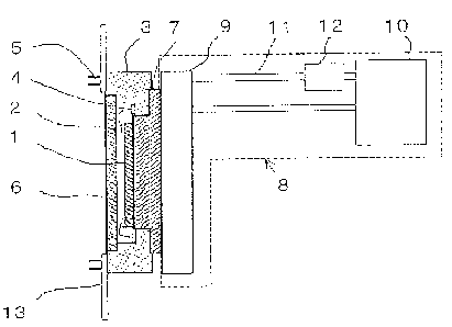
Fig. 1 is a sectional view of one embodiment (first
embodiment) of a device of the present invention. An image
pick-up element 1 is manufactured by a deposition, sputtering,
a thin film forming technique of a CVD or a thin film processing
technique such as etching. The image pick-up element 1
includes a light receiving surface composed of a plurality
of pixels having light receiving elements for generating
signals corresponding to the luminance of an incident light,
and a signal accumulating part that is provided in the pixels
or in the vicinity thereof and accumulates the signals
respectivelygeneratedbythe lightreceiving elements during
a shooting or photographing operation. Further, after the
shooting operation is completed, the signals accumulated in
the signal accumulating part are outputted.
[0013]
An element mounting part 7 is made of a copper tungsten
alloy and an element storing part 3 is made of aluminum nitride
(AIN) . These members are air-tightly bonded together to be
formed integrally. The image pick-up element 1 is stuck to
7
CA 02547376 2006-05-18
the element mounting part 7. The thermal conductivity of the
copper tungsten alloy is 200 W/m. k and higher than the thermal
conductivity (150 W/m.k) of the aluminum nitride (AIN).
Accordingly heat generated in the element mounting part 7 can
be efficiently discharged outside.
[0014]
An electrode 2 for applying a driving voltage to operate
the image pick-up element and taking out the signals
accumulated in the image pick-up element is connected to an
electrode 4 formed inside the element storing part by wire
bonding. The electrode 4 is connected to a control circuit
board 13 for controlling the image pick-up element 1 by
inputting and outputting pins 5 provided in the light receiving
surface side.
[0015]
A cooling mechanism 8 comes into contact with the back
surface of the element mounting part 7. The cooling mechanism
8 includes a heat absorbing part 9 for absorbing heat generated
in the image pick-up element 1, a heat radiating part 10 for
radiating the heat absorbed by the heat absorbing part 9 to
atmospheric air, a piping 11 for connecting the heat absorbing
part 9 to the heat radiating part 10, and a pump 12 for
circulating cooling water in the piping. The cooling
mechanism 8 may be replaced by a different cooling mechanism
from that of this embodiment, for instance, other systems
S
CA 02547376 2006-05-18
employed as the related art such as an air cooled type in which
a heat radiating plate is provided on the back surface of the
element storing part to supply air to the heat radiating plate
by a fan or the like or an electronic type for absorbing heat
by a Peltier effect.
[0016]
A window material 6 made of transparent glass is stuck
to a part opposed to the light receiving surface of the image
pick-up element 1. Since the window material is stuck to the
part opposed to the light receiving surface, the image pick-up
element is prevented from being deteriorated owing to the
adhesion of dirt or dust to the light receiving surface of
the image pick-up element . Further, in this embodiment, the
element storing part 3 is air-tightly stuck to the window
material 6 under a dry nitrogen atmosphere. Thus, nitrogen
is sealed in the element storing part to prevent the
deterioration of the element due to the entry of water.
[0017]
Another embodiment (second embodiment) of the present
invention is shown in Fig. 2. Tn Fig. 2, the same components
as those of Fig _ 1 are designated by the same reference numerals
and a detailed description thereof is omitted. In the second
embodiment, inputting and outputting pins 5a are provided on
side surfaces of an element storing part 3. The inputting
and outputting pins 5a are provided on the side surfaces of
9
CA 02547376 2006-05-18
the element storing part 3, so that a control circuit board
13 does not need to be attached to the front surface of a window
material 6. Accordingly, an optical system such as a lens
can be attached more closely to an image pick-up element
assembly.
[0018]
In the above-described embodiment, the image pick-up
element having the signal accumulating part is mentioned.
However, it is to be understood that even if other image pick-up
element than the above-described image pick-up element is
mounted on an element mounting part, this image pick-up element
is included in claims of the present invention.
It will be apparent to those skilled in the art that
various modifications and variations can be made to the
described preferred embodiments of the present invention
without departing from the spirit or scope of the invention.
Thus, it is intended that the present invention cover all
modificationsandvariationsofthisinventionconsistentwith
the scope of the appended claims and their equivalents.